Note: Descriptions are shown in the official language in which they were submitted.
12~3S9
HIGH-SPEED DYNAMIC CMOS CIRC~IT
-
The invention is a high-speed dynamic CMOS circuit, and
more particularly, a dynamic CMOS circuit capable of low-power
operation at very high speeds in logic array, memory array and
multiplexer applications.
The increasing demand for high-speed performance in the
major building blocks of VLSI circuits, including memory arrays,
programmable logic arrays and multiplexers, has brought about
rapid development in circuit techniques. Dynamic CMOS logic has
been used successfully in the implementation of these circuits to
provide maximum speed capability with low area cost. In
programmable logic arrays (PLAs) dynamic CMOS logic is used in
both the AND and OR planes to enhance performance. It is also
used for the decoder sections of multiplexers and memory arrays.
Dynamic CMOS logic consists of a n-transistor logic
structure having an output node which is pre-charged to VDD by a
p-transistor (precharge phase) and conditionally discharged by a
n-transistor (evaluate phase). It may alternatively consist of a
p-transistor logic structure having an output node which is
pre-charged to VSS by a n-transistor and conditionally discharged
by a p-transistor. In the case of two-plane dynamic CMOS logic
PLAs, multiplexers and memory arrays, the output of a n-transistor
logic structure input plane is directly connected to a
n-transistor logic structure output plane through intermediate
logic using a multi-phase clock strategy. The intermediate logic
consumes area and slows down the operation of the overall circuit.
The circuit of the invention dispenses with the
intermediate logic and the multi-phase clock strategy, and has a
correspondingly reduced area and improved speed. The basic gate
of the invention consists of a n-transistor logic structure whose
output node is discharged to VSS prior to evaluation and is
conditionally charged by a p-transistor during evaluation.
Programmable logic array, multiplexer and memory array circuits
may be configured using the basic gate of the invention.
In a first form, the invention is a two-plane logic
array circuit adapted to be operated from a single clock pulse
train and having an input plane and an output plane. The input
12983sg
plane is defined by an array of rows and input columns, and the
output plane is defined by an array of the rows and at least one
output column. A series of first transistors is selectively
positioned in the input plane at the intersection of the rows with
the input columns such that a charge on one of the input columns
results in the discharge of any charge on those rows sharing first
transistors with that column. The circuit further comprises
first, second, third, fourth and fifth gate means. The first gate
means controls transmission of each of a first set of input
signals to a respective one of the input columns. The second gate
means controls the discharge of charge stored on the rows. The
third gate means and the state of the input columns controls the
charging of each of the rows with a respective one of a second set
of input signals. The state of the rows controls the discharge of
charge from the at least one output column. The fourth gate means
controls a pre-charging of the at least one output column, and the
fifth gate means controls the transmission of the state of the at
least one output column to the output of the logic array circuit.
The first, second and fourth gate means open and close
simultaneously, and the fifth gate means opens and closes as the
first gate means closes and opens respectively. The logic array
circuit further comprises a subcircuit for deriving a third gate
means pulse train from the single clock pulse train for
controlling the opening and closing of the third gate means.
During a first time period the first, second and fourth gate means
are opened and then closed, and the fifth gate means is closed and
then opened. The first set of input signals is thereby
transmitted to a respective one of the input columns, any charge
on the rows is discharged, and the at least one output column is
pre-charged. The third gate means remains closed during the first
time period. During a second time period the third gate means is
opened and then closed, the first, second and fourth gate means
remain closed, and the fifth gate means remains open. The state
of each row is thereby determined by the state of the respective
second input signal and the state of the input columns. The state
of the at least one output column is then determined by the
resultant state of the rows, and the resultant state of the at
least one output column is then transferred to the output of the
--2--
12g~359
logic array circuit. The aggregate length of the first and second
time periods is equal to the period of the single clock pulse
train.
One circuit of the first form of the invention is a
programmable logic array circuit in which the second set of input
signals are all in a high state and are adapted to charge those
rows which do not share first transistors with charged first
columns. Another circuit of the first form of the invention is a
multiplexer circuit in which the first set of input signals is
utilized for selecting one of the rows and in which the at least
one output column is a single output column. In this circuit, the
state of that one of the second set of input signals associated
with the selected row is passed to the output of the logic array
circuit.
The first time period may have a length slightly greater
than one-half of the period of the single clock pulse train. The
first, second, fourth and fifth gate means may each be open for a
time equal to one-half of the period of the single clock pulse
train. The third gate means may be open for a time approximating
one-eighth of the period of the single clock pulse train.
A second form of the invention is a memory circuit. The
input plane of the memory circuit corresponds to the input plane
of the multiplexer circuit already described, except that the
third gate means connects each of the rows to a charge source
rather than to the input signals of the multiplexer. Each of the
rows represents a discrete memory address selected by a unique set
of values on the input columns. The first, second and fourth gate
means function in a similar manner to those in the programmable
logic array and multiplexer circuits previously described. The
output columns of this circuit are paired, each output column pair
being connected to a series of storage elements. Each of those
storage elements is associated with a respective row of the memory
circuit through a pair of gates associated with that row. Each
pair of output columns forms the inputs to a comparator having its
output connected to the input of a fifth gate means, the output of
which is the output of the memory circuit. The memory circuit
also has a sixth gate means and a seventh gate means for
controlling the input of data to the pairs of output columns. The
1~9~3~9
sixth gate means is connected between the data to be input and an
intermediate input, and the seventh gate means is connected
between the intermediate input and the output columns. The first,
second, fourth and sixth gate means open and close simultaneously.
The fifth gate means is open during the time that a read/write
signal is in the read mode and the first gate means is closed.
The seventh gate means is open during the time that the read/write
signal is in the write mode and the first gate means is closed.
As with the first form of the invention, the memory circuit has a
subcircuit for deriving a third gate means pulse train from the
single clock pulse train for controlling the opening and closing
of the third gate means. During a first time period the first,
second, fourth and sixth gate means are opened then closed, either
the fifth or seventh gate means is closed then opened, and the
third gate means remains closed. One gate means of the fifth and
seventh gate means is closed then opened, and the other gate means
of the fifth and seventh gate means remains closed. The selection
signals are thereby each transmitted to a respective one of the
input columns for selecting one of the rows, any charge on the
rows is discharged, the pairs of output columns are charged, and
the state of the data input is transferred to the intermediate
input of the memory circuit. During a second time period the
third gate means is opened then closed, the first, second, fourth
and sixth gate means remain closed. One gate means of the fifth
and seventh gate means remains open, and the other gate means of
the fifth and seventh gate means remains closed. The selected row
thereby assumes a charged state, and each pair of output columns
is connècted to a respective storage element associated with the
selected row. The state of the pairs of output columns is
transferred to the output of the memory circuit when the
read/write signal is in the read mode, and the state of the
intermediate input is transferred to the pairs of output columns
when the read/write signal is in the write mode. The aggregate
length of the first and second time periods is equal to the period
of the single clock pulse train.
The invention will next be described in terms of a
preferred embodiment utilizing the accompanying drawings, in
which:
129~3~9
Figure 1 is a schematic diagram of a prior art circuit
having a pair of dynamic CMOS gates and intermediate logic
connecting those gates, the prior art circuit requiring two clock
input signals.
Figure 2 is a schematic diagram of a prior art
programmable logic array circuit constructed from the dynamic CMOS
gates and intermediate logic illustrated in Figure 1.
Figure 3 is a typical timing diagram of the two clock
input signals utilized with the circuits of Figures 1 and 2.
Figure 4 is a schematic diagram of a typical circuit
used to obtain the two clock input signals required by the circuit
of Figures 1 and 2.
Figure 5 is a schematic diagram of a circuit having a
pair of dynamic CMOS gates of the invention and a timing signal
generator for creating the two clock input signals required by the
CMOS gates of the invention.
Figure 6 is a timing diagram of the clock input signals
created by the circuit of Figure 5.
Figure 7 is a schematic diagram of a programmable logic
array circuit utilizing the dynamic CMOS gates of the invention.
Figure 8 is a schematic diagram of a multiplexer circuit
utilizing the dynamic CMOS gates of the invention.
Figure 9 is a schematic diagram of a memory array
circuit utilizing the dynamic CMOS gates of the invention.
The diagram of Figure 1 is based on a description of a
prior art two-phase dynamic CMOS circuit at pages 358 and 359 of
'Principles of CMOS VLSI Design --- A Systems Perspective' by Neil
Weste and Kamran Eshraghian (Addison-Wesley Publishing Company,
1985).
The prior art basic dynamic CMOS circuit of Figure 1 has
a pre-charge phase occurring when first clock input 01 is high.
Pre-charge p-transistor 12 opens and n-transistor 13
simultaneously closes. Charge passing through p-transistor 12
then pre-charges node 14. The second clock input 02 is
maintained high during the pre-charge phase, forcing the output D
of NOR gate 15 to maintain a low state irrespective of the state
of node 14. The inputs A, B and C are allowed to change during
the pre-charge phase, but must remain constant at other times. As
lZ~3359
clock input ~1 falls, transistors 12 and 13 close and open,
respectively. If any one of the inputs A, B and C is in a high
state, the charge on node 14 will discharge to ground; otherwise,
node 14 will maintain a high state. The two-phase clocking scheme
is set up such that clock input ~2 will not go low before the
state of node 14 has stabilized. The value on node 14 is
transferred through inverter 16 to the input of NOR gate 15, and
after clock input ~2 has gone low the value at output D of NOR
gate lS assumes the value on node 14. Node 17 is carrying a
charge (having been pre-charged at the same time as node 14), and
the value on output D of NOR gate 15, along with the value on
inputs E and F, determines the O~TP~T value at node 17 during the
evaluate phase (when clock inputs ~1 and ~2 are both low).
Figure 2 illustrates a programmable logic array
constructed using the two-phase dynamic CMOS logic of Figure 1.
The logic array has an AND plane and an OR plane. The AND plane
has a series of input gates 20, each controlled by the first clock
input ~1 of the two-phase clock. A pair of inverters 21 and 22
are connected serially to the output of each gate 20. The outputs
of inverters 21 and 22 are connected to an inverted input column
line 23 and a non-inverted input column line 24, respectively.
The circuit of Figure 2 has a pair of row lines 25 each of which
is connected to a power voltage VDD through a pre-charge
p-transistor 26. A pair of ground lines 27 are connected to VSS
through a series of n-transistors 28. The gate of each pair of
transistors 26 and 28 are connected through an inverter (not
shown) to first clock input ~1 A series of first logic
transistors 30 are each selectively positioned such that its
channel extends between a row line 25 and a ground line 27, and
its gate is connected to either an inverted column line 23 or a
non-inverted column line 24. Each row line 25 is connected to the
input of an inverter 31, the output of which is one of the inputs
to a two-input NOR gate 32. The other input to each NOR gate 32
is second clock input ~2. The OR plane has a pair of output
column lines 33 each connected to VDD through a p-transistor 34,
and has a pair of ground lines 35 each connected to VSS through a
n-transistor 36. The gate of each pair of transistors 34 and 36
are connected through an inverter (not shown) to first clock input
l~g~3~9
~1 A series of second logic transistors 37 are each selectively
positioned such that its channel extends between an output column
line 33 and a ground line 35, and its gate is connected to a row
line 25. Each output column line 33 is connected to the input of
an output gate 38 controlled by second clock input ~2. The
output of each gate 38 then passes through an inverter 39. When
each of the input gates 20 is open, ie. when clock input ~1 is
high, the state of the three inputs A, B and C appears in inverted
form on each of the input column lines 23 and in non-inverted form
on each of the input column lines 24. Each of the input column
lines 23 and 24 may be connected to the gate of one or more of the
first logic transistors 30. When one of the input column lines 23
and 24 is in a high state, the first logic transistors 30
connected to that column line are turned on to connect a
respective row line 25 with the associated ground line 27. During
this phase the pre-charge transistors 26 are turned on and the
transistors 28 are turned off, so that any row lines 25 and ground
lines 27 connected to 'on' logic transistors 30 are charged to
VDD. The state of the row lines 25 does not affect the OR plane
because clock input ~2 is high. Clock input ~1 then goes low,
the pre-charging of the AND plane and OR plane is terminated, and
any row lines 25 connected to 'on' logic transistors 30 are
discharged. By the time that clock input ~2 goes low, the input
signals have propagated through the AND plane logic. The state of
each row line 25 is then passed to the OR plane. Each row line 25
may be connected to the gate of one or more of the second logic
transistors 37 in the OR plane, and determines which of the output
column lines 33 are discharged to ground through the transistors
36. As an example output of the programmable logic array of
Figure 2, the S output would be equal to (A.B.C)+(A.C).
Figure 3 illustrates two typical clock inputs ~1 and ~2
used by the circuits of Figures 1 and 2, and Figure 4 illustrates
a typical circuit for creating the two clock inputs from an
external CLOCK input having a period of 2t1. The external CLOCK
input is fed into a J-K master/slave flip-flop 41 to create clock
input ~1' which has one-half the frequency of the external CLOCK
input. The external CLOCK input and clock input ~1 are fed into
an OR gate 42 to form clock input ~2. With the circuit of Figure
~29~3359
4, clock input ~2 goes low half-way through the evaluate phase of
clock input ~1 One half of the evaluate phase (equal to the
aggregate time t2+t3 in Figure 3) is used for stabilizing the AND
plane logic before the AND plane output is passed to the OR plane
logic. Time t2 is the time taken for the signal level at node 14
to change in the AND plane, and time t3 is a time margin added to
ensure stability prior to clock input ~2 going low. Time t2 is
typically made equal to time t3. The other half of the evaluate
phase (equal to the aggregate time t4+t5 in Figure 3) is available
for passing signals through the OR plane. Time t4 is the time
taken for the signal level at node 17 to change after clock inpu-t
~2 has gone low, and time t5 is wasted time. This prior art
circuit requires two external CLOCK inputs to pass a signal from
its input to its output. As will subsequently become evident, the
time margin t3 is not needed with the circuit of the invention,
which requires only a single external CLOCK input to pass a signal
from its input to its output.
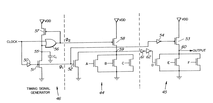
Figure 5 illustrates a basic embodiment of the dynamic
CMOS logic circuit of the invention, comprising a pair of basic
logic gate circuits 44 and 45 driven by a timing signal generator
circuit 46. Figure 6 illustrates the two clock inputs ~1 and ~2
created from the external CLOCK input by timing signal generator
circuit 46.
The basic embodiment of Figure S operates in the
following way. Passing the external CLOCK input through driver 50
creates the clock input ~1' and that clock input drives
n-transistors 51 and 52, and also drives p-transistor 53 through
inverter 54. When the external CLOCK input is high, transistors
51, 52 and 53 are all turned on. Capacitor Cl discharges through
transistor 51, and node 55 drops to a low state. The output of OR
gate 56, which is clock input ~2' is high and transistors 57 and
58 are turned off. Any charge on node 59 is discharged to VSS,
while node 60 is simultaneously pre-charged to VDD through
transistor 53. When the external CLOCK input goes low,
transistors 51, 52 and 53 turn off. OR gate 56 has two low
inputs, and clock input ~2 goes low. Pre-charge transistors 57
and 58 turn on, and capacitor Cl starts to charge. Capacitor C
is sized so as to ensure that clock input ~2 remains low a
129l~33~9
sufficient time for charge passing through transistor 58 to
evaluate logic gate circuit 44; that time is typically in the
order of one-eighth of the period of the external CLOCK input.
After capacitor Cl has charged, one input of OR gate 56 is high;
clock input ~2 then goes high and the transistors 57 and 58 turn
off. The logic inputs A, B and C are evaluated while transistor
58 is on. If one of those inputs is high, node 59 assumes the
ground state; otherwise, node 59 assumes a high state. Node 59 is
connected to input D of the OR plane as shown in Figure 5, and
would normally also be connected to the inputs of other logic gate
circuits 45. In order to minimize the load capacitance on node
59, the output of logic gate circuit 44 is normally buffered by a
pair of drive inverters 61 and 62. Input D propagates with inputs
E and F through circuit 45 to create an O~TPUT value. When the
external CLOCK input returns high, transistors 51, 52 and 53 turn
on, clock input ~2 is not affected, and the process earlier
described is repeated. The circuit of the invention does not
require the time margin of the prior art circuit, and the time
required for signals to pass from the input of circuit 44 to the
output of circuit 45 is equal to the period of one external CLOC~
cycle, ie. half of the time required for signal propagation
through the prior art circuit.
The designations TIME PERIOD 1 and TIME PERIOD 2 have
been placed in Figure 6 to assist in describing the relationship
between clock inputs ~1 and ~2. Although the aggregate of TIME
PERIOD 1 and TIME PERIOD 2 is equal to the period of the external
CLOCK input, TIME PERIOD 2 is slightly shorter than TIME PERIOD 1.
Figures 7, 8 and 9 illustrate three circuits embodying
the clocking scheme of the invention. All three circuits utilize
a signal generator circuit corresponding to circuit 46. Figure 7
is a diagram of a programmable logic array circuit having logic
comparable to that in the prior art circuits of Figures 2. Figure
8 is a diagram of a multiplexer circuit, and Figure 9 is a diagram
of a memory circuit.
With respect to the programmable logic array circuit of
Figure 7, each of the inputs A, B and C is fed into an input
transmission gate 63 controlled by clock input ~1 The output of
gate 63 is connected to an inverted input column line 64 through a
1298;~59
first inverter 65. The output of first inverter 65 is connected
to a non-inverted input column line 66 through a second inverter
67. The circuit of Figure 7 has a series of input column lines 64
and 66, row lines 68, output column lines 69, first logic
transistors 70 and second logic transistors 71 similar to those
earlier described with respect to Figure 2. The circuit of Figure
7 also has a series of transistors 72 each having its channel
extending between one of the row lines 68 and VSS and having its
gate connected to clock input ~1 Charge passes from VDD to the
row lines 68 through a series of transistors 73 each having its
gate connected to clock input ~2. Charge passes from VDD to the
output column lines 69 through a series of transistors 74 each
having its gate connected to clock input 01 through an inverter
75. Each of the output column lines is connected to an output
transmission gate 76 controlled by clock input ~1 through an
inverter 77. The outputs of the gates 76, when inverted by a
series of inverters 78, represent the output of the programmable
logic array circuit.
The programma~le logic circuit of Figure 7 operates in
the following way. When clock input ~1 goes high, the state of
the inputs A, B and C are placed on the respective input column
lines 64 and 66, any charge on the row lines 68 is discharged
through the transistors 72, and the state of the outputs on the
inverters 78 becomes the outputs S, T, U and V. Clock input ~1
then goes low, preventing any change on the inputs A, B and C from
affecting the input column lines 64 and 66, and turning off the
transistors 72. The transistors 74 turn off, terminating the
pre-charging of the output column lines 69. Clock input ~2 then
goes low for a short time, allowing each of the transistors 73 to
pass charge from VDD. The charge is retained on those row lines
68 which are connected to first logic transistors 70 that are all
in the 'off' state. The state of the row lines 68 determines
which of the output column lines 69 retain their charge, a high
state on a row line 68 resulting in the second logic transistors
connected to that row line discharging the charge from any
connected output column lines 69. Since each of the gates 76 is
open, the state of the output column lines 69 appears inverted at
the output of the inverters 78. When clock input ~1 goes high,
--10--
~zg83~9
the process repeats. As with the basic circuit of Figure 5, a
buffer means must be placed between the output of the AND plane
and the input of the OR plane. Each driver 79 in Figure 7 is
formed from a pair of drive inverters having a construction and
function corresponding with the inverters 61 and 62 earlier
described with respect to Figure 5.
The multiplexer circuit of Figure 8 operates in a
similar fashion. With this circuit, the inputs A, B and C each
act to select one of the row lines 80, 81 or 82, respectively.
For instance, an (A,B,C) value of (1,0,0) selects row line 80.
When clock input ~2 goes high, the state of the D input is
maintained on row line 80. The state of the E and F inputs are
not retained on row lines 81 and 82, because an (A,B,C) value of
(1,0,0) results in any charge that enters row lines 81 and 82
being dissipated through transistors 83 and 84. The state of row
line 80 determines the state of the output column line 85 after
pre-charging through transistor 86. If row line 80 is high,
output column line 85 goes low; if row line 80 is low, output
column line 85 stays high. The state of the S output is the
inverse of the state of output column 85. If (A,B,C) has the
value (0,1,0), the S output will assume the value on the E input
after one cycle of the external CLOCK input.
With respect to the memory circuit of Figure 9, the
pairs of gates 90, 91 and 92 are open when clock input ~1 is
high. The pair of gates 90 pass the address selection values
(ADDRl,ADDR2) to the pairs of inverters 93 and 94. An
(ADDRl,ADDR2) value of (l,l) selects row line 95, and an
(ADDRl,ADDR2) value of (0,0) selects row line 96. With clock
input ~l high, the pair of gates 91 are open for grounding row
lines 95 and 96, and the pair of gates 92 pass input data values
INl and IN2 to the pairs of inverters 97 and 98.
After clock input ~1 goes low, clock input ~2 goes low
and then high. If row line 95 is selected, it remains in a high
state after clock input ~2 returns high. A high state on row
line 95 results in the opening of transistors 100, 101, 102 and
103. During a write operation, the complementary state of the
output column lines 105 and 106 will determine the state of the
storage unit 108, and the complementary state of the output column
--11--
12~3~9
lines 110 and 111 will determine the state of storage unit 112.
If the READ/WRITE (R/W) input is low (for a write cycle), the
output of AND gate 115 goes high when clock input ~1 goes low
(that clock input and R/~ input being inverted by the inverters
116 and 117, respectively). Transistors 120, 121, 122, and 123
are then in an open condition. Transmission gates 124 and 125
will remain closed during the time that the R/W input is low since
the output of AND gate 126 remains in a low state during that
time. With transistors 100, 101, 102, 103, 120, 121, 122 and 123
all 'on', the values on the pairs of inverters 97 and 98 are
passed to the storage units 108 and 112. The former value on each
of the storage units 108 and 112 is either maintained or is
'flipped'. As clock input ~1 returns high, the transistors 100,
101, 102, 103, 120, 121, 122 and 123 are turned off, and the
15 values on storage units 108 and 112 can no longer be affected. If
the R/W input is high (for a read cycle), the output of AND gates
115 and 126 go low and high, respectively, as clock input ~1 goes
low. Transistors 120, 121, 122 and 123 thereby remain closed
throughout the read cycle. Transistors 100, 101, 102 and 103 and
20 transmission gates 124 and 125 are open during that portion of the
read cycle in which clock cycle ~1 is low. The values on storage
units 108 and 112 are passed to the respective pairs of inputs of
comparators 128 and 129, respectively, and appear at the output of
inverters 130 and 131, respectively. Those outputs, designated as
OUTl and OUT2 in Figure 9, are unaffected by the return of clock
input ~1 to the high state. Each of the transistors 132 is a
NMOS transistor driven by the clock input ~1 directly; in
contrast, each of the corresponding pre-charge transistors in the
circuits of Figures 7 and 8 is a PMOS transistor driven by the
inverted clock input ~1 The difference results from the fact
that the noise margins required on the output column lines of the
circuits of Figures 7 and 8 are not re~uired for the circuit of
Figure 9 because of the presence of comparators 128 and 129. For
proper performance of the memory circuit, the R/~ input should not
change its state during the time that the external CLOCK input is
in the low state.
The programmable logic array, multiplexer and memory
circuits that have been described are all capable of operating
-12-
" lZ9l~359
with the single-phase clock input. Very high clock speeds (in the
order of 100 MHz with existing technology) may be used with these
circuits.
-13-