Note: Descriptions are shown in the official language in which they were submitted.
1298391
Backqround of the Invention
1. Field of the Invention
The invention relates to electro-optical
switches, and in particular to switches which exhibit a
step-like response to switching voltage.
2. DescriPtion of the Prior Art
The present invention relates to electro-optical
switches for switching a beam of optical radiation between
two waveguides on a substrate. Optical waveguides are
typically fabricated from a pyroelectric material such as
lithium niobate or lithium tantalate or from semiconductor
materials such as gallium arsenide or indium phosphide.
Wavepaths or waveguides are generally fabricated in the
substance by depositing a dopant such as titanium on the
surface of the substrate in the pattern desired for the
wavepaths. The substrate is then heated to diffuse the
dopant into the substrate. This procedure forms a
wavepath or waveguide, i.e., a section in the pyroelectric
material that guides light, usually about 3 to 10 um wide.
To permit logic operations, signal processing, or
switching between wavepaths in the pyroelectric material,
an electric field is imposed across the region of the
crystal where a change in beam direction is desired. Such
a field is generated by electrodes deposited on the
substrate for this purpose. The field produces local
changes in the optical polarizability of the crystal, thus
locally changing the refractive index and, in turn,
altering the path of light through the crystal.
In one form of integrated optics switch and
modulator, known as a directional coupler switch, a pair
of waveguides of refractive index greater than the
surrounding substrate are provided in close parallel
relationship to one another with electrodes provided
thereon. Unfortunately, in many substances such as
lithium niobate (LiNbO3) and lithium tantalate (LiTaO3)
the modulators and switches so formed have proven to be
polarization sensitive. For example, while light having a
lZ9839~
- 2 -
direction of polarization perpendicular to the substrate
plane can be substantially modulated or switched, light
with a polarization parallel to the substrate plane is
simultaneously disadvantageously unaffected or relatively
unaffected.
Switches in the form of directional couplers,
preferably manufactured on a GaAs base or a LiNbO3 base,
and whereby the control arrangement essentially is formed
by a single controllable DC voltage supply are disclosed
in:
1. "Optical Waveguide Connecting Networks", H. F. Taylor,
Electronics Letters, Vol. 10, No. 4, February 21,
1974, pp. 41-43;
2. "Electro-Optic Y-Junction Modulator/Switch",
Electronics Letters, Vol. 12, No. 18, Sept. 2, 1977,
pp. 459-460;
3. "Experimental 4 x 4 Optical Switching Network",
Schmidt et al, Electronics Letters, Vol. 12, No. 22,
October 28, 1976, pp. 575-577;
4. "Metal-Diffused Optical Waveguides in LiNbO3", Schmidt
et al, Applied Physics Letters, Vol. 25, No. 8, Oct.
15, 1974, pp. 458-460;
5. "A New Light Modulator Using Perturbation of
Synchronism Between Two Coupled Guides", Tada et al,
Applied Physics Letters, Vol. 25, No. 10, Nov. 15,
1974, pp. 561-562;
6. "GaAs Electro-Optic Directional-Coupler Switch",
Campbell et al, Applied Physics Letters, Vol. 27, No.
4, August 15, 1975, pp. 202-205;
7. "Electrically Switched Optical Directional Coupler:
Cobra", Papuchon et al., Applied Physics Letters, VG1 .
27, No. 5, September 1, 1975, pp. 289-291;
8. "Electro-Optically Switched Coupler with Stepped DELTA
Beta Reversal Using Ti-diffused LiNbO3 Waveguides",
Schmidt et al, Applied Physics Letters, Vol. 28, No.
9, May 1, 1976, pp. 503-506;
9. "Electrically Active Optical Bifurcation: BOA",
-~ iZ9839~
Papuchon et al, Applied Physics Letters, Vol. 31, No.
4, August 15, 1977, pp. 266-267.
Electro-optic switches are interferometric in
nature, i.e., they require a precise phase shift to
achieve a switched state with low crossstalk. The
directional coupler switch, for example, requires a phase
shift of \l3n between its two waveguides to switch.
Because of small fabrication errors, this phase shift
requires slightly different voltages for each switching
element in a switching array. It is also very difficult
to obtain switching in the two orthogonal polarizations
simultaneously.
Other electro-optical switches are described in:
1. "Guided-Wave Devices for Optical Communication", R. C.
Alferness, IEEE Journal of Quantum Electronics, Vol.
QE-17, No. 6, June 1981, pp. 946-958;
2. "Polarization~Independent Optical Directional Coupler
Switch Using Weighted Coupling", R. C. Alferness,
Appl. Phys. Lett. 35 (10), 15 November 1979 pp. 748-
750;
3. "Optical-Waveguide Hybrid Coupler," M. Izutsu, A.
Enokihara, T. Sueta, optics Letters, November 1982
Vol. 7, No. 11 pp. 549-551;
4. "Electrically Active Optical Bifurcation: BOA" M.
Papuchon and A. M. Roy, Appl. Physics Letters, Vol.
31, No. 4 15 August 1977, pp. 266,267;
5. "Digital-Controlled Electro-optic lx2 Switch for
Time-Division Multiplexing and Data Encoding", K. T.
Koai and P. L. Liu, Applied Optics, Vol. 25, No. 22,
15 November, 1986, pp. 3968-3970:
6. "4x4 Ti: LiNbO3 Integrated Optical Crossbar Switch
Array", L. McCaughan and G. A. Bogert, Appl. Phys.
Lett., 47 (4), 15 August 1985, pp. 348-350;
The most useful switch by far has been the directional
coupler switch. It has the following drawbacks:
1. It requires a precise voltage to define the switch
states. This voltage may change slightly in time, and
`~ lZg8391
-- 4 --
vary from device to device due to fabrication
variations.
2. It usually operates only on one polarization state.
It is very difficult (although demonstrated) to build
a polarization insensitive directional coupler.
3. It is wavelength sensitive; it will operate
satisfactorily only on a narrow wavelength range.
4. It is sensitive to fabrication tolerance. Some of
this sensitivity may be removed by using a "delta beta
reversal" switch (Reference 8) at the price of having
to control a voltage source for precise switching.
Other switches suffer from similar problems. The proposal
to synthesize a switch which will have a digital response
has also been made. This synthetic switch is very
complicated and still has many drawbacks. Prior to the
present invention, there has not been a switch which is
simultaneously:
1. Insensitive to switching voltage variations. (This
makes this switch particularly attractive for use in
switch arrays where a single voltage source can be
used.)
2. Insensitive to fabrication variations.
3. Provides simultaneous switching of two orthogonal
polarization components.
4. Permits operation over a broad wavelength range.
SummarY of the Invention
Briefly, and in general terms, the invention
provides an electrically controlled electro-optical switch
having a step-like response to the switching voltage
including;
an input waveguide and first and second output
waveguides for propagating optical radiation disposed on
an electro-optical substrate.
Electrodes are disposed on the substrate and are
~ iZ9839~
responsive to a control voltage applied thereto for
producing an electrical field so that the velocity of the
optical radiation propagated in the waveguides is affected
and the direction of the propagation of the optical
radiation is switched from the first output waveguide to
the second output waveguide in a step-like manner as a
function of time and the control voltage applied to the
electrodes.
DescriPtion of the Preferred Embodiment
Most of the switches demonstrated or proposed in
integrated optics are very different from their
electronics counterpart in their response. While an
electronic switch has a sharp step-like response to the
switching voltage, all integrated optics switches show a
varying response, where "pure" switched states are
obtained only at very specific values of the applied
voltage. For example, in a directional coupler switch,
switching is obtained at two distinct voltages VO and V1.
This requires precise control of the voltage, and in
practice the exact switching voltage is expected to vary
from device to device due to process variations. A
"digital" switch would ideally have two switched states
which are not sensitive to the exact voltage. The present
invention provides such a switch in integrated optics by
using an asymmetric x-junction or 2x2 structure. For
integrated optics a step-like response eliminates the need
for precise voltage control for switching and permits the
operation of many such elements by a single voltage
source, such as required for switching arrays. Moreover,
because such characteristics should apply to both
polarizations in a LiNbO3 device, the switch can be made
polarization independent.
The device according to the present invention is
based on an asymmetric waveguide junction structure,
composed from two input guides of unequal width, a
double-moded central region and a symmetric output
branching.
1298391
, .
An asymmetric waveguide branching is known to
perform mode sorting. The fundamental or first order mode
of the central region can be excited by launching light
through the wider or the narrower input guides,
respectively. The input guides have different widths so
they excite different normal modes at the two-mode region
of the junction. An electric field applied to the
otherwise equal output branches generate the required
asymmetry to guide each of the modes to a different output
waveguide. The advantage of such a design is that the
switching response is improved with an increasing
asymmetry, and therefore one obtains a step-like response
as is required from a digital switch.
The symmetry of the output branching is broken
by the external electric field. These modes can now be
routed to the required output guide by properly biasing
the output branching. The fundamental mode will be
directed to the arm with higher index of refraction. Due
to the symmetry breaking operation, switching is not
periodic or quasiperiodic, but depends only on the
direction of the bias.
The switching response can be used to generate a
polarization independent switching in Ti:LiNbO3. In
common x- or z-cut LiNbO3 devices one polarization is
affected by an electro-optic interaction which is three
times weaker than the other polarization. It is obvious
that in a switch with the above response both
polarizations can be switched by a strong enough bias.
Brief DescriPtion of the Drawinq
FIG. 1 shows a schematic layout of the proposed
switch. It is composed of a waveguide junction with two
input guides of different width converging into the
junction and two identical guides diverging out of it. An
external electrical field can be applied using the
electrode structure. Switching is accomplished by biasing
the symmetric output branch so that the refractive index
~ ~298391
of one guide is increased and that of the other guide is
decreased. Light from the wider input waveguide will be
routed to the output guide with the higher index of
refraction. A calculation of light output as a function
of the induced index difference, (which is proportional to
the strength of the applied field), can be made
demonstrating a step-like response.
Such a structure is directly implementable in
x-cut lithium niobate shown in FIG. 1 through the
established technology of waveguide fabrication by
titanium indiffusion. For a switch to operate at the
important wavelength range of 1.3 - 1.5 micrometers the
waveguide width should be in the range of 5 - 10 microns.
For proper operation the angle between the waveguides
should be of the order of 1 - 5 milliradians. A smaller
angle will make the switch longer, but requires smaller
electric fields for switching. The electrodes can be
either evaporated or electroplated and may be of gold, but
a number of other metals can be used as well.
The same design, with a minor change, can be
implemented also in z-cut lithium niobate as will be shown
in FIG. 2. The change required is in the shape of the
electrode pattern.
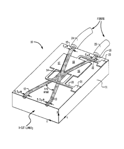
Turning to FIG. 1, there is shown a perspective
view of a substrate on which the electro-optical switch 10
according to the present invention can be implemented.
More particularly, the Figure depicts a substrate 11
composed of x-cut or lithium niobate. (The drawing shows
an x-cut LiNbO3 geometry.) A first waveguide 12 and a
second waveguide 13 are provided on the substrate 11. The
first waveguide 12 preferably has a width of 6.5 microns
while the second waveguide 13 preferably has a width of
5.5 microns. Although the preferred embodiment shows
converging waveguides with different widths, they may
alternatively be different in some other parameter leading
to different propagation velocity of the guided light, or
the two diverging guides may be identical in all respects
--~ 1298391
-- 8 --
but can be made different by properly biasing them with an
electric field.
The waveguides 12 and 13 are normally spaced
from one another on the substrate 11, but approaching the
central region 14 the waveguides 12 and 13 are arranged to
converge at an angle between one and five milliradians.
The waveguides 12 and 13 converge at the central region 14
in which light from both the first 12 and second 13
waveguides propagate. The central region 14 forms a
waveguide junction, supporting two modes. An electric
field can be applied along all or some of these input and
output waveguides through properly placed electrodes, so
that light from the converging input waveguides 12 and 13
can be switched between the two diverging output
waveguides 15 and 16.
Alternatively, in another embodiment a structure
may be provided in which the input side is composed only
of one waveguide which then splits into the two diverging
waveguides. The electric field is applied to one or both
of the diverging guides. (This is known as a lx2 switch).
In the preferred embodiment, a first output
waveguide 15 and a second output waveguide 16 are provided
on the surface of the substrate 11; the output waveguides
are spaced from one another but are connected to and
diverge from the central region 14. The width of the
first output waveguide 15 is preferably 6 microns while
the width of the second waveguide is also preferably 6
microns.
There is further provided means for generating
an electrical field composed of electrodes disposed on the
surface of the substrate adjacent the central region 14.
More particularly, the present invention provides a first
electrode consisting of a first portion 17 and a second
portion 19 which are electrically connected by means of a
bus line 20 which is connected to a pad 21 on the surface
of the substrate. A second electrode 18 is also provided
which is disposed on the surface of the substrate adjacent
129839~
-
to the central region 14. The second electrode 18 is
connected to a bus 22 which is in turn connected to a
pad 23 on the surface of the substrate. An electrical
potential may then be provided to the electrodes on the
substrate by means of wires which may be connected to
pads 21 and 23 according to wire bonding techniques known
in the art.
The electrode 17, consists of a trapezoidal-
shaped structure having one edge running parallel to the
length of the first output waveguide 15. The second
portion 19 of the first electrode also consists of a
trapezoidal-shaped structure having one edge running
parallel to and along the length of the second output
waveguide 16.
The second electrode 18 preferably consists of a
triangularly-shaped layer having one edge disposed along
the length of the first output waveguide 15 and a second
edge disposed along the length of the second output
waveguide 16. The edge of the first electrode 17 adjacent
the output waveguide 15 is spaced apart and parallel to
the edge of the second electrode 18, also, extending along
the length of the waveguide 15. The edge of the second
portion of the electrode 19 is spaced apart and runs
parallel to the edge of the second electrode 18 which
extends along the length of the waveguide 16.
The first and second output waveguides 15 and 16
may be coupled to similar switches 10 or other elements in
an integrated optic circuit. Alternatively, the output
waveguides 15 and 16 may be directly attached to optical
fibers 24 and 25 respectively, such as shown in a highly
diagramatic fashion in the Figure.
Turning next to FIG. 2, there is shown an
alternative embodiment of the present invention which is
implemented on a substrate consisting of z-cut lithium
niobate. The Figure shows a first input waveguide 12 and
a second input waveguide 13 converging into a central
region 14 such as that depicted in FIG. 1. A first output
-` ~Z98391
-- 10 --
waveguide 15 and a second output waveguide 16 are also
shown diverging from the central region 14 as depicted in
the first embodiment. The width and other characteristic
of such waveguides for such second embodiment are similar
to that shown in the first embodiment and need not be
described in detail here. The configuration of electrodes
in the second embodiment is somewhat different. The first
electrode 26 consists of a plate having an edge portion
extending along a portion of the first input waveguide 12,
a portion of the central region 14 and over a portion of
the output waveguide 15. The first electrode 26 is
connected to a pad 28 for receiving a dc electric signal
from external to the substrate. The second electrode
portion 27 which is connected to a pad 29, consists of a
plate disposed on the substrate including a portion
extending at the edge of the central region 14 and over
the second output waveguide as it diverges from the
central region 14.
The electrodes are disposed over a silicon
dioxide or some other transparent layer, in order to
optically isolate them from the waveguides. My invention
can be implemented in other electro-optic integrated
optics material such as GaAs, InP etc. It is also
important to note that a number of variations on the above
structure may be conceived without affecting its basic
operation. For example, the electrode can operate on only
one of the output guides. The input and output sides of
the switch can be interchanged, and in another version
both the input and the output may be acted upon by
electric field. My invention covers all these and other
possible variations.
An integrated electro-optic switch as this one
should find application in future optical networks where
direct switching of the optical signal will be required.
This switch is likely to be an element in a switch array
which can handle a large number of input channels.
While the invention has been illustrated and
lZ9839^1
described as embodied in electro-optical switch, it is not
intended to be limited to the details shown, since various
modifications and structural changes may be made without
departing in any way from the spirit of the present
invention.
Without further analysis, the foregoing will so
fully reveal the gist of the present invention that others
can readily adapt it for various applications without
omitting features that from the standpoint of prior art,
fairly constitute essential characteristics of the generic
or specific aspects of this invention, and, therefore,
such adaptations should and are intended to be
comprehended within the meaning and range of equivalence
of the following claims.