Note: Descriptions are shown in the official language in which they were submitted.
This invention relates to a microwave converter,
more particularly, to improvements in a circuit
configuration for developing a small-sized and compact
microwave converter for satellite broadcasting.
Recently, satellite broadcasting by a microwave
converter using a broadcasting satellite has been put into
practice, and microwave devices which have been used mainly
in the industrial field are entering the consumers' field.
One example of one such device is a microwave converter for
receiving satellite broadcasting. Such a microwave
converter has a function as converting a received signal of
a UHF band to an IF signal.
Satellite broadcasting is aimed to be received by
homes so that a large-sized antenna having a large diameter
and used in a satellite communication system is not
necessary. In satellite broadcasting, therefore, a large
amount of power is used for transmission when compared with
that used in satellite communication. This enables the use
of a small-sized receiving antenna. However, in order to
receive the signals readily at homes with little expense, a
satellite broadcasting reception system which employs a
smaller antenna than currently used had to be developed. In
attempting to solve this problem, a highly efficient
antenna, as well as an excellent microwave converter used in
connection thereto, have been extensively studied.
With the development of a small-sized antenna, a
small-sized and compact microwave converter to be associated
with such an antenna had to be developed. Generally, a
microwave converter is connected to a primary radiator
disposed at a radio focal point of the antenna aperture
surface. The primary radiator and microwave converter are
supported by a support member extending from an antenna
pedestal. When used outdoors, the primary radiator and
microwave converter may vibrate because of wind, rain or
other elements of nature causing a shift from the focal
point, thereby lowering the receiving efficiency. In order
to prevent this problem from arising, the support member
should be designed to have sufficient strength and
. .. .. .
2~6~9
durability. It is necessary to design such a support member
to be simple, lightweight and inexpensive, so that the
support member is adaptable to a small-sized antenna.
microwave converter of the prior art is considerably bulky
and heavy. If such a microwave converter is used,
therefore, it is very difficult to solve the above-mentioned
problem. Thus, an effective means for solving such a
problem is to develop a small-sized and compact microwave
converter. It will be appreciated that the realization of
a small-sized and compact microwave converter is also
effective with respect to the development of a simple,
light, handy and inexpensive antenna system even when a
conventional antenna is used.
A microwave converter consists mainly of a low
noise amplifier, filter, mixer, local oscillator, IF
amplifier, power supply, etc. These circuit components
except the IF amplifier and power supply are formed by MIC
(Microwave Integrated Circuits) which are mainly constructed
by microstrip circuits. A significant factor for developing
a small-sized and compact microwave converter lies in
arranging the circuit components effectively.
This invention will be better understood and its
numerous objects and advantages will become apparent to
those skilled in the art by reference to the accompanying
drawings as follows:
Figure 1 is a perspective view showing the first
embodiment of a microwave converter according to the
invention;
Figure 2 is a partial perspective view of the
embodiment of Figure l;
Figure 3 is a perspective view showing the second
embodiment of a microwave converter according to the
invention;
Figure 4 is a perspective view showing the third
embodiment of a microwave converter according to the
invention;
Figure 5 is a partial perspective view of the
embodiment of Figure 4;
A
, ..~
86~1
~3
Figure 5 is a side view showing the fourth
embodiment o a microwave converter according to the
invention.
Figures 7A and 7B are side views showing the fifth
embodiment of a microwave converter according to the
invention;
Figure 8 is a perspective view showing the sixth
embodiment of a microwave converter according to the
invention;
Figures ~A and 9B are side views showing the
seventh embodiment of a microwave converter according to the
invention;
Figure 10 is a plan view illustrating
schematically the internal arrangement of a prior art
microwave converter;
Figure llA is a plan view of another example of a
prior art microwave converter;
Figure llB is a side view of the microwave
converter of Figure llA.
According to the invention, circuit components of
a microwave converter are mounted on dielectric boards which
are assembled into a three-dimensional structure, and
therefore the converter can be made compact. A plurality of
circuit boards can be arranged three-dimensionally on the
flat surfaces of a conductive body surrounding a local
oscillator, greatly reducing the overall dimensions of the
microwave converter lengthwise and breadthwise. That is,
peripheral spaces enclosing the local oscillator having a
metal shield case, which previously has not been used as the
spaces for arranging circuit components in a prior art
microwave converter, can now be used effectively as the
spaces for arranging the circuit components. Thus, most of
the spaces which have been useless in a prior art microwave
converter can be utilized as the spaces for arranging the
circuit components, thus enabling the development of a
small-sized and compact microwave converter.
Microwave converters of the prior art will be
described in more detail with reference to the drawings.
. ...
-~ ~Z986~g
Figure 10 shows a view illustrating schematically the
internal arrangement of a prior art microwave converter. In
the microwave converter, a microwave signal is transmitted
from a waveguide coaxial converter 1 to a low noise
amplifier 2 through a microwave signal input terminal 7, and
further to a mixer 4 through a filter 3. In the mixer 4,
the microwave signal is then mixed with a local oscillating
signal from a local oscillator 5, thereby converting the
signal at the microwave frequen¢y to an IF signal. The IF
signal is sent to an IF amplifier 6, and the output signal
of the IF amplifier 6 is then supplied via an output
terminal 8 to a demodulator (not shown). A power supply 9
supplies a bias voltage to each circuit. The low noise
amplifier 2, filter 3, local oscillator 5, etc. are formed
on a dielectric board 10 using mainly microstrip circuits.
The circuit components may be assembled integrally on one
board or substrate, or they may be assembled individually on
a plurality of boards which are then assembled on a base.
Since frequencies of the IF amplifier 6 and power supply 9
are relatively low, they may be formed on a separate board.
In the prior art example shown in Figure 10, the main
circuit components are arranged on a flat surface.
Figures llA and llB show another example of a
conventional microwave converter. In the figures, similar
reference numerals of Figure 10 indicate similar circuit
components. In the microwave converter of Figures llA and
llB, the circuit components are arranged on two flat
surfaces. Each of the main circuit components is formed
individually on a board. Some of the components are mounted
on one surface of a base 11, and the other components on the
opposite surface of the base 11. The base ll is usually
made of a metal plate. The microwave converter of Figures
llA and llB operates in the same manner as that of Figure
10, and, therefore, its detailed explanation is omitted.
The circuit components 2, 3 and 4 arranged on the upper
surface of the base 11 may be integrally arranged on one
dielectric board. Alternatively, the circuit components 2,
lZ~86~L~
3 and 4 and the IF amplifier 6 may be integrally arranged on
one dielectric board.
The local oscillator 5 shown in Figures 10 and llB
has an oscillation resonator which is usually a dielectric
resonator of the electromagnetic field coupling type.
Hence, the local oscillator 5 is enclosed in a metal shield
case so that the deterioration of the properties of the
oscillator, the fluctuation in oscillation frequency caused
by external disturbances, and unwanted radiation due to the
local oscillator output may be prevented. Consequently, the
local oscillator 5 is constructed in a bulky structure which
is large in height as compared to the other circuit
components used in the microwave converter.
In the examples of the prior art described above,
the following problems are encountered with respect to the
development of a small-sized microwave converter.
As shown in Figures 10, llA and llB, the circuit
components constituting a microwave converter are arranged
flatly so that the overall size of the microwave converter
tends to become larger lengthwise and breadthwise.
Moreover, the local oscillator 5 protrudes largely because
it must be enclosed in a metal shield case. The other
circuit components can be formed with the height lower than
the hsight of the metal shield case so that the height of a
microwave converter depends upon the height of the metal
shield case, resulting in that the overall dimensions of the
converter become large, particularly in height. It has been
desired to develop a novel circuit configuration which can
solve the aforementioned problems so as to construct a
smaller microwave converter.
The microwave converter of this invention, which
overcomes the above-discussed and numerous other
disadvantages and deficiencies of the prior art, comprises
circuit components, including a local oscillator, wherein
the circuit components except at least the local oscillator,
are mounting on at least one of the outer surfaces of a
three-dimensional body. The inner surfaces of the body
.t~
~ ~ZSIi~6~
constitute a groundin~ surface, and said local oscillator is
disposed on one of said inner surfaces.
In a preferred embodiment, the output terminal of
said local oscillator is electrically connected to one of
said circuit components formed on the outer surfaces via a
hole formed in said body.
In a pre~erred embodiment, the body is made of a
dielectric material.
In a preferred embodiment, the dielectric body
consists of a plurality of dielectric boards.
In a preferred embodiment, the local oscillator is
disposed on the inner surface of one of said dielectric
boards.
In a preferred embodiment, the dielectric body
consisting of said plurality of dielectric boards has a U-
shaped section.
In a preferred embodiment, two of said boards the
inner surfaces of which are facing to each other are
extended, an additional dielectric board facing to the outer
surface of the board disposed between said two boards is
provided. The additional board is connected to said
extended portions of the two boards, and the inner surfaces
of the extended portions and the inner surface of said
additional board constitute grounding surfaces which enclose
one or more circuit components formed on said board disposed
between said two boards.
In a preferred embodiment, the one or more circuit
components formed on said board disposed between said two
boards are electrically connected to circuit components
formed on said two boards, via holes formed in said extended
portions.
The microwave converter of this invention
comprises circuit components including a local oscillator,
wherein said local oscillator is disposed in a hollow
portion formed in an electrically conductive body, said
circuit components are formed on at least one board each of
which is disposed on one outer surface of said conductive
body.
9~3~gL9
In a preferred embodiment, the output terminal of
said local oscillator is electrically connected to one of
said circuit components via a hole formed in said body and
said board.
In a preferred embodiment, the body is made of a
dielectric material.
In a preferred embodiment, the body has a cubic
shape.
In a preferred embodiment, the body has a trigonal
prism-like shape.
Thus, the invention described herein makes
possible the objects Of: (1) providing a microwave
converter which is small in size; (2) providing a
microwave converter in which circuit components are
compactly assembled; and (3) providing a microwave
converter in which a local oscillator is disposed without
outwardly protruding.
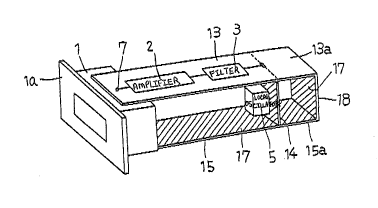
Figure 1 shows the first embodiment of the
invention. In the microwave converter, a signal from a
waveguide coaxial transducer 1 having a mounting flange la
is picked up by an antenna and directed to an input tarminal
7 disposed above ths waveguide coaxial transducer 1. Tha
microwave converter comprises three component dielectric
boards 13, 14 and 15 which are assembled to form a U-shaped
structure~ The inner surfaces of the dielectric boards 13
to 15 are lined with copper foil 17 which are electrically
connected to form a common ground surface. Printed circuits
are formed on the outer surfaces of the dielectric boards 13
to 15. An amplifier 2 and filter 3 are disposed on the
outer surface of the first dielectric board 13, a mixer 4
~Figure 2) on the outer surface of the second dielectric
board 14, and an IF amplifier 6 on the outar surface of the
third dielectric board 15. A local oscillator 5 is disposed
in the space surrounded by the three dielectric boards 13 to
15. The lead of the oscillator 5 penetrates the dielectric
board 14 via a through hole 14h (Figure 2) and is soldered
to the circuit pattern formed on the outer surface of the
dielectric board 14. Thereby, the local oscillator 5 is
. ". ~
~2~86~9
-
electrically connected to the mixer 4 and supported by the
second dielectric board 14. These exemplified
configurations for interconnecting the circuit components
formed on the boards are used mainly for transmitting high
frequency signals. Hence, the supply of a bias voltag~ from
a power supply to other circuit components can be conducted
by a cable.
The through hole may be replaced with a simple
hole. Alternatively, the case of the local oscillator 5 may
be fixed to the inner surface of the second dielectric board
1~, and connected to the mixer 4 on the outer surface by a
cable extending through the hole.
In the above-described arrangement, the mixer 4 is
disposed on one surface of the second dielectric board 14
and the local oscillator 5 on the opposite surface of the
dielectric board so as to sandwich the dielectric board 14
therebetween. Both are connected with each other through
the second dielectric board 14, thereby enabling the output
of the local oscillator 5 to be supplied to the mixer 4 by
an extremely short distance. Due to the fact the local
oscillator 5 is enclosed by at least three component
dielectric boards 13, 14 and 15 as mentioned above, the
shielding effect to the local oscillator 5 can be greatly
improved. Since the outer surfaces are substantially flat,
moreover, useless spaces can be eliminated.
Among the circuit patters formed on the outer
surfaces of the dielectric boards 13 to 15, the circuit
patterns constituting the signal transmission lines must be
connected at each interface of the dielectric boards. The
reference A in Figure 2 indicates the connecting portion of
the circuit patterns between the dielectric boards 13 and
14. The transmission circuits on the dielectric boards 13
and 14 are connected with each other, e.g. by soldering,
while they remain on the outer surfaces of the dielectric
boards.
In the first embodiment having the above-described
configuration, the microwave signal of about 12 GHz given
from the input terminal 7 passes the amplifier 2 and filter
'~ " '
3L298~9
3 on the first dielectric board 13, and then turns at a
right angle to proceed to the mixer 4 on the second
dielectric board 14 to be converted down to an IF signal o~
1 GHz. The IF signal from the mixer 4 turns at a right
angle to enter into the IF amplifier 6 on the third
dielectric board 15, and ad~ances to the output terminal 8
(Figure 3~ after amplification b~ the IF amplifier 6. In
this embodiment, the signal advances three-dimensionally (in
a U-shaped course) along the three-dimensional structure
formed by the dielectric boards 13 to 15. The circuit
patterns are formed on the outer surfaces, and the ground
surface on the innex surfaces. This arrangement may be
reversed. Namely, the ground plane may be formed on the
outer surfaces, and the circuit patterns on the inner
surfaces.
The second embodiment of the invention is shown in
Figure 3. This embodiment is constructed in the same way as
the first embodiment of Figure 1 except that the third
dielectric board 15 constitutes another side of a cubic
body, i.e. it lies perpendicular to both the first and
second dielectric boards 13 and 14. In Figure 3, the
numeral 8 indicates the output terminal.
Figure 4 shows the third embodiment of the
invention. The third embodiment is also similar to the
first embodiment, however the first dielectric board 13 and
third dielectric board 15 are extended. The extended
portions 13a and 15a are connected with each other by a
fourth dielectric board 18 which is parallel to the second
dielectric board 14. The inner surfaces of the extended
portions 13a, 15a and fourth dielectric board 18 are lined
with copper foil 17 for grounding. According to the
configuration of the third embodiment, the mixer 4 which is
formed on the second dielectric board 14 is shielded by the
extended portions 13a, 15a and fourth dielectric board 18.
In such a configuration, some measures must be taken to
connect the signal transmission circuits 1~ and 20 which are
formed on the first dielectric board 13 and the second
dielectric board 14. In Figure 5, an L-shaped metal piece
.~Z98~i~9
21 is soldered to both the signal transmission circuits 19
and 20 through a hole 22 formed in the first dielectric
board 13. The metal piece 21 may be substituted by a
solder.
Figure 6 illustratas another configuration for
connecting the signal transmission circuits in which the
circuits are connected by a metal piece 23 inserted in a
through hole 24. In the fourth embodiment shown in Figure
6, the through hole 24 is formed in the first dielectric
board 13. The metal piece 23 may be replaced with a solder
filled in the hole 24. A reinforcing metal piece 25 is
disposed, as shown in Figure 6, to bs in contact with the
inner surfaces of the dielectric boards 13, 14 and 15,
thereby increasing the reliability of the connection between
the grounding surfaces and also improving the mechanical
strength of the cubic body.
In the embodiments of Figures 1 to 5, a shield
case may be disposed individually on the outer surface of
each dielectric board. Additionally, a further shield case
enclosing the entire microwave converter may be provided.
Moreover, one or more boards for reinforcement or heat
radiation may be attached to a side surface of the
dielectric boards 13, 14 and 15.
Figures 7A and 7B show the fifth embodiment of the
invention. The microwave convarter of Figures 7A and 7B has
a rectangular shape as a whole. In this embodiment, the
local oscillator 5 is disposed in a hollow space 12a formed
in a rectangular body 12 which is electrically conductive.
On each of four outer surfaces of the conductive body 12,
30 four dielectric boards 13, 14, 15 and 16 are disposed
respectively. The low noise amplifier 2 and filter 3 are
formed on the first dielectric board 13; the mixer 4 on the
second dielectric board 14; the IF amplifier 6 on the third
dielectric board 15; and a power supply 9 on the fourth
35 dielectric board 16. The circuit components 2 to 4, 6 and
9 are disposed on the outer surfaces of the boards 13 to 16.
The inner surfaces of the boards 13 to 16 are basically
conductive surfaces for grounding, and are bonded to the
~L29~36~
outer surfaces of the conductive body 12 which function as
the ground so that the boards 13 to 16 are commonly
grounded. The output of the local oscillator 5 is connected
to the input terminal ~`or locally oscillating signals of the
mixer 4 formed on the second board 14, by a connecting
conductor via a hole penetrating both the conductive body 12
and the second board 14.
In the foregoing embodiment, the four boards 13 to
16 are disposed three-dimensionally on four outer surfaces
of the conductive body 12, and the local oscillator 5 is
situated in the inner space 12a of the conductive body 12.
Therefore, useless spaces are eliminated such that a high
density mounting can be accomplished, resulting in a small-
sized and compact microwave converter. Moreover, a leakaga
of the local oscillating signal radiated from other than the
output terminal of the local oscillator 5 can be effectively
shielded because the local oscillator 5 is disposed in the
conductive body 12. The way of arranging the local
oscillator 5 in the conductive body 12 and the position of
its output terminal are not restricted to the above, and can
be selected adequately as required.
Figure 8 shows the sixth embodiment of the
invention in which the conductive body 12 is formed into a
trigonal prism-like shape. The conductive body 12 has a
hollow space in which the local oscillator is disposed. The
four dielectric boards 13 to 16 on which circuit components
are arranged are disposed three-dimensionally on the outer
surfaces of the prism-like conductive body 12. Due to such
a unique arrangement, circuit components can be mounted more
densely, resulting in a smaller microwave converter as
compared with that o~ Figures 7A and 7B.
A microwave converter for satellite broadcasting
in which a further embodiment of the invention is employed
i5 illustrated in Figures 9A and 9B. This embodiment is a
modification of the embodiment shown in Figure 7. The
dielectric boards 13, 15 and 16 disposed on the outer
surfaces of the conductive body 12 which encloses the local
oscillator 5 are extended. The extended portions of the
3 ;~9~
12
boards are connected to the waveyuide coaxial converter 1 so
that the rectangular portion of the coaxial converter 1 is
surrounded by the three boards 13, 15 and 16.
Other kinds of circuit components can be used in
a microwave converter of the invention. A plurality of
dielectric boards may be replaced with a three~dimensional
dielectric body.
Although microwave converters for satellite
broadcasting have been described as embodiments of the
invention, the circuit configuration according to the
invention can be advantageously applied to other various
microwave equipments.
It is understood that various other modifications
will be apparent to and can be readily made by those skilled
in the art without departing from the scope and spirit of
this invention. Accordingly, it is not intended that the
scope of the claims appended hereto be limited to the
description as set forth herein, but rather that the claims
be construed as encompassing all the features of patentable
novelty that reside in the present invention, including all
features that would be treated as equivalents thereof by
those skilled in the art to which this invention pertains.
,
.,