Note: Descriptions are shown in the official language in which they were submitted.
~ X~
~ ,. .
l~CKGROUND OF ~HE INVENTION
Fiel~l of the lnvention
The present invention relates generally to a semiconductor l~lser device. It is
specifically directed to an improved semiconductor device which, due to a difference
between the refractive index of the waveguide portion and the neighboring region results in
optical confinement of the emitted light so that the width of the region through which the
electrical current passes can be reduced.
Brief Description of the Drawings
The present invention will be described more completely in conjunction with the
accompanying drawings of a preferred embodiment of the invention. These drawings are
strictly for the purpose of explanation and understanding only.
Figure I is an expanded sectional view of a first preferred embodiment of a
semiconductor laser device produced according to the present invention;
Figure 2 is a cross-sectional view taken along the line 11-11 of Figure l;
Figure 3 is a graph showing the relationship between the thickness d of the plate
portion of the cladding layer and the difference ~ N in retractive index with respect to
various effective thicknesses of guiding layer (GL) in a semiconductor laser device with a
ridged waveguide stmcture;
Figure 4 is a graph of the dit`ference ~, N in refractive index versus the eft`ective height
of the strip str~lcture with respect to various eftective thicknesses of guiding layer in a
semiconductor laser having a strip waveguide structure;
Figure S is a graph of the relationship between the clifference A N in refractive index
due to the ridged waveguide structure and the thickness d ot the p]ate portion of the
cladding layer in which the total difference in refractive index due to the ridged and strip
waveguide structures is within the allowable range ol~ from 0.008 to 0.0lS;
Figure 6 is a expanded sectional view of a second preferred emhodiment o-t a
semiconductor laser device according to the present invention.
Figure 7 is an expanded perspective view of a prior art semicondnctor laser device
with a ridged waveguide structure; and
Figure 8 is an expanded perspective v;ew of a prior art semiconductor laser device
with a strip waveguide structure.
~.
~L~98~4~l
DESCRIPTION OF THE PR~Ol~ ART
The prior art ;ncludes sem;conductor ]aser dev;ces having a ridged waveguide
structure ;n which th~ w;dth of the current pass;ng reg;on is red~lced. ReFerr;ng to F;gure
7, there is shown a distributed feedback semiconductor laser (DFB laser) in which a r;dged
wavegu;de structure ;s employed. The structure ;ncludes a semiconductor substrate 50 of
a given conductivity type made, for example, of an n-type GaAs, having a major surface.
A sem;conductor cladd;ng layer 52 having the same conductivity type as the sem;conductor
substrate 50 and composed, for example, of an n-type AlGaAs is formed on the major
surface of the substrate 50 by means of epitaxial growth. An active semicond~lctor layer 54
made, for example, of GaAs, ;s then formed on the cladding layer 52 ;n the same manner.
A semiconductor guiding layer 56
- lA-
jtr~ \
9~6~1
having a conductivity opposite to that of the cladding layer 52
and composed, for example, of a p-type AlGaAs is formed on the
active layer 54 in the same manner. A periodically corrugated
surface which serves as a diffraction grating 58 is formed on the
surface of the guiding layer 56 opposite from the active layer
54. The diffraction grating covers the entire surface of the
guiding layer and is composed of corrugations which extend
laterally, are triangular in cross section, and have a regular
pitch interval. After the diffraction grating 58 is formed on
the guiding layer 56, a semiconductor cladding layer 60 of the
same conductivity characteristics as the guiding layer 56 and
composed, for example, of a p-type AlGaAs is formed on the
guiding layer 56 by means of epitaxial growth. Then, a
semiconductor cap layer of the same conductivity type as the
cladding layer 60 and composed, for example, of a p-type GaAs is
formed on the cladding layèr 60 in the same manner. An etching
process is performed selectively to remove both side regions of
the cap layer 62 and the cladding layer 60, leaving a central
region thereof extending in the longitudinal direction, and the
entire lower region of the cladding layer 60, the cap layer 62
comprising only the central region. The cladding layer 60 has a T-
shaped cross section. As a result, a stripe structure is formed by
the cap and cladding layers 62 and 60. The surfaces of the removed
portions of the cap and cladding layers 62 and 60 are covered with
insulation films 64. The top surface of the cap layer 62 and the
bottom surface of the substrate 50 are provided with counter
electrodes 66 and 68 so as to establish ohmic contacts.
In this type of semiconductor laser device, the flow of
current can be restricted to a narrow current passing region.
However, this type of device does not provide good optical
--2--
confinement. In order to achieve good optical confinement, the
device must be designed to have about 0.01 difference in the
refractive index between the central waveguide region and the
neighboring region. This difference depends on the effective
thickness of the guiding layer 56 (GL) and the thickness d of the
neighboring region of the cladding layer 56. However, it is
difficult to obtain the desired difference in refractive index by
adjusting the thicknesses since the allowable error is so
small. Therefore, a device of this type cannot be produced which
has consistently predictable optical confinement characteristics.
There has also been proposed a DFB laser having a waveguide
which comprises a narrow strip for obtaining uniform and
reproducible optical confinement characteristics. One such
device is illustrated in Figure 8 and includes a semiconductor
substrate 70 of a given conductivity type composed, for example,
of a n-type GaAs, having a major surface. A semiconductor
cladding layer 72 of the same conductivity type as the substrate
70 and composed, for example, of n-type AlGaAs is formed on the
major surface of the substrate 70 by means of epitaxial growth.
An active semiconductor layer 74 composed, for example, of GaAs
is then formed on the cladding layer 72 in the same manner. A
semiconductor guiding layer 76 having conductivity
characteristics opposite to that of the cladding layer 72 and
made, for example, of a p-type AlGaAs is formed on the active
layer 74 in the same manner. Then, a corrugated strip 78 having
a regular period of repitition and which serves as a diffraction
grating is formed on the surface of the guiding layer 76 opposite
to the active layer 74. Corrugated strip 78 extends over the
central region of the guiding layer 76 in a longitudinal
~Z9~
direction. The strip 78 defining the diffraction grating is
composed of corrugations having a regular pitch and extending
perpendicularly to the longitudinal axis thereof. After the
diffraction grating 78 is formed on the guiding layers 76, a
semiconductor cladding layer 80 of the same conductivity
characteristics as the guiding layer 76 and formed, for example,
of a p-type AlGaAs is formed on the guiding layer 76 by way of
epitaxial growth. Then, a semiconductor cap layer 82 of the same
conductivity characteristics as the cladding layer 80 and
composed, for example, of a p-type GaAs is formed on the cladding
layer 80 in the same manner. Thereafter, ion implantation is
performed by injecting ions such as boron ions or the like from
the cap layer 82. High resistance current restricting regions 84
are formed on both sides of the cap layer 82 so as to insulate
the sections adjacent to central region extending in the
longitudinal direction. A pair of counter electrodes 86 and 88
are provided on the top surface of the cap layer 82 and the
bottom surface of substrate 70 to establish ohmic contacts
therebetween.
This type of semiconductor laser device effectively achieves
good optical confinement due to the differences in the refractive
indices of the respective sections thereof. However, the current
passing region cannot be made narrow so as to increase the
reactive current since there is no mechanism for restricting the
flow of current to a well defined area within the cladding layer
80.
The aforementioned disadvantages of the semiconductor laser
device having a ridged waveguide structure or the narrow strip
can also be observed in conventional Fabry-Pe~rot semiconductor
lasers.
-4-
SUMMARY OF THE INVENTION
The present invention seeks to eliminate the aforementioned
disadvantages and to provide a semiconductor laser device which
can effectively achieve good optical confinement due to
differences in refractive indices, and which also has a narrow
current passing region. These effects can be consistently
obtained in the devices of the present invention.
In order to accomplish these results, a semiconductor laser
of the present invention includes ridge structures and a strip
which is defined in the light guide.
More specifically, the semiconductor laser device of the
invention may include a semiconductor substrate having a cladding
layer thereon of the same conductivity type. A laser active
layer is disposed on the cladding layer on the side opposite from
the semiconductor substrate. A second semiconductor layer of the
opposite conductivity type is disposed on the laser active layer
and has a strip waveguide structure for obtaining optical
confinement. The strip waveguide structure projects from the
second semiconductor layer on the opposite side from the laser
active layer and extends to the central area of the second
semiconductor layer in a longitudinal direction. A third
semiconductor cladding layer of the second named conductivity
type is disposed on the strip waveguide. A third semiconductor
cladding layer having a ridged waveguide structure for defining
the current passage region extends in the longitudinal direction
with a width which corresponds to the strip structure. A fourth
semiconductor layer of the second conductivity type is disposed
on the ridge waveguide structure, and a pair of electrodes is
included for supplying a bias voltage, one being connected to the
semiconductor substrate and the other to the fourth semiconductor
--5--
layer.
The refractive index of the third semiconductor cladding
layer differs from that of the neighboring region due to the
difference in thicknesses so that the center region serves as an
optical waveguide. The difference between the refractive indices
of the center and neighboring regions may be approximately 0.01
and is preferably in the range from 0.008 to 0.015. The
difference in refractive index due strictly to the strip
waveguide structure is preferably from 0.007 to 0.013. The
ridged structure may project in a perpendicular direction to the
third semiconductor cladding layer. The third semiconductor
layer may have a plate portion and a ridged portion and has a T-
shaped cross section. The thickness of the plate portion may be
approximately equal to or less than 5,000A. The thickness of the
third semiconductor is approximately 15,000A. The strip
waveguide structure may project in a perpendicular direction with
respect to the second semiconductor layer. The semiconductor
laser device may comprise a Fabry-Pe'rot laser device. The strip
waveguide structure may have a periodically corrugated surface
which serves as a diffraction grating. The grating may be
composed of laterally extending corrugations of regular pitch and
of essentially triangular cross section.
In accordance with another phase of the present invention,
there is provided a distributed feedback semiconductor laser
device which includes a semiconductor substrate of a first
conductivity type and a semiconductor cladding layer of the same
conductivity type located on the major surface of the
semiconductor substrate. A laser active layer is disposed on the
cladding layer on the side opposite from the semiconductor
substrate. A second semiconductor layer of opposite conductivity
gL2~B E;9~
type is disposecl on the laser active layer and includes a strip wavegu;de structure having a
periodically varying corrugated surf~ce which serves as a dif*action grating. The strip
wavegu;de structure projects from the second semiconductor layer on the side opposite from
the laser active layer and extends over the central area of the second semiconductor layer
in a longitudinal direction. The corrugated surface has corrugations which extend in a lateral
direction perpendicular to the longitudinal direction. A third semiconductor cladding layer
of the opposite conductivity type is disposed on the strip waveguide structl.lre and has a ridge
waveguide structure for defining an electrical current passing region. The ridge structure
projects from the side opposite to the second semiconductor layer and extends in the
longitudinal direction. A fourth semiconductor layer of the opposite conductivity type is
disposed on the ridge waveguide structure and a pa;r of electrodes is included for supplying
bias voltage, one of the electrodes being connected to the semiconductor substrate and the
t~e fcurth semicond-lctor lay~r.
~ \
- 7 -
~9~4~
DESCRIPrrION OF T~IE PREFEI~l~ED EMBODIMENTS
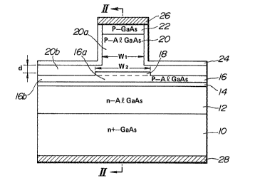
Referring to the drawings, particularly to Fig-lres 1 and 2, the preferred embodiment
of a distributed feedback semiconductor laser accord;ng to the present invention includes
a semiconductor substrate 10 haVillg one COtldUCtiVity type, such as arl n-type GaAs which
has a major surface. A semiconductor cladding layer 12 of the Sclllle conductivity type as the
je 10, and preferably
~r~ r~
"~
~2~6~
consisting of n-type AlGaAs is formed on the major surface of the
substrate by means of epitaxial growth. An active semiconductor
layer 14 composed, for example, of intrinsic GaAs, is then formed
on the cladding layer 12 in the same manner. A semiconductor
guiding layer 16 of the second conductivity type opposite to that
of the cladding layer 12 is formed on the active layer 14 in the
same manner. The guiding layer 16 may consist, for example, of a
p-type AlGaAs. A periodically corrugated strip 18 serving as a
diffraction grating is formed on the surface of the guiding layer
16 opposite from the active layer 14. The corrugated strip
extends over the central area of the surface of the guiding layer
16 in a longitudinal direction whose width is W2. The guiding
layer 16 consists of a thicker central portion 16a on which the
corrugated strip 18 is formed and a pair of thinner plate
portions 16b formed on either side of the corrugated strip 18.
The effective thickness of the central portion 16a of guiding
layer 16 which defines the waveguide is thicker than that of the
plate portion 16b. The corrugated strip 18 is composed of
corrugations which are essentially triangular in cross section,
have a regular pitch, and extend perpendicular to the
longitudinal axis of the strip. After the corrugated strip 18 is
formed on the guiding layer 16, a semiconductor cladding layer 20
of the same conductivity as that of the guiding layer 16 and
composed of a p-type AlGaAs, for example, is formed on the
guiding layer 16 by way of epitaxial growth so as to cover the
entire surface including the thicker central portion 16a and the
thinner plane surface of the guiding layer 16. The band gap of
the cladding layer 20 is larger than that of the guiding layer 16
and the active layer 14. A semiconductor cap layer 22 having the
same conductivity as that of the cladding layer 20 and made of a
_g_
~2~ 41
p-type GaAs, for example, is formed on the cladding layer 20 in
the same manner. Thereafter, an etching process is performed to
selectively remove the side portions of the cap layer 22 and the
cladding layer 20 to a predetermined depth. A central portion of
the cap layer 22 and a portion of the cladding layer 20 having a
T-shaped cross section remain after the etching process. The
cladding layer 20 comprises a ridged portion 20a having a width
Wl and a plate portion 20b having a thickness d. The ridged
portion 20a projects upwardly from the guide layer 16 at a
location corresponding to the corrugated strip 18 and extends in
the longitudinal direction. The cap layer remains only at the
top of the ridged portion 20a. As a result, a ridged waveguide
structure is formed by the cap and cladding layers. The surfaces
of the removed portions of the cap and cladding layers 22 and 20
are covered with insulation films 24. Moreo~ver, the top surface
of the cap layer 22 and the bottom surface of the substrate 10
are provided with electrodes 26 and 28 so as to establish ohmic
contacts therebetween, respectively.
The DFB laser of the present invention has characteristics
of both the ridged and strip structures. The characteristics of
such a laser device will now be described.
The thickness of the ridge portion should be two or more
times that of the plate portion in order to sufficiently prevent
the flow of electrical current from spreading laterally and to
keep the current flow restricted to a narrow area. The ridged
structure differs from a mesa electrode structure in that the
thickness d of the plate portion 20b of the cladding layer 20 is
equal to or less than about S,OOOA and the thicknesses of the
ridge portion 20a of cladding layer 20 and the cap layer 22 are
about 15,000A and 5,000A respectively, whereas the thickness d is
--10--
~2~
more than about 10,000~ in the mesa structure. As will be
described below, the magnitude of difference between the
refractive indices of the ridged and plate portions 20a and 20b
of the cladding layer begins to be significant when their
thicknesses have the aforementioned values. The ridged structure
may restrict the flow of electrical current to a narrow region
more effectively than does the mesa structure.
In order to achieve the desired electrical current
restricting effect, the difference ~ N between the refractive
indices of the ridged and plate portions should be at least about
0.01. Since the allowable range of refractive index
difference ~ N is, from experience, from 0.08 to 0.015, a
difference ~N in this range will be considered below.
Figure 3 shows the relationship between the thickness d of
the plate portion of the cladding layer and the magnitude of
difference ~ N in refractive index, with respect to various
effective thicknesses of guiding layer tGL) in the ridge
waveguide structure semiconductor laser device. Figure 4 shows
the difference ~ N in refractive index related to the effective
height of the strip structure with respect to various effective
thicknesses of suiding layer in the strip waveguide structure
semiconductor laser.
Figure 5 shows the relationship between the difference ~N in
refractive index to the ridged waveguide structure and the
thickness d of the plate portion of cladding layer 20 on the
basis of Figures 3 and 4, in which the total difference ~ N in
the refractive index due to the ridged and strip waveguide
structures is within the allowable range. In Figure 5, the
curved lines a and b correspond to ~ N equals 0.08 and ~ N equals
O.OlS, respectively. The thickness d of the plate portion of the
~2~364~L
cladding layer is assumed to be less than 5,000A in the ridged
waveguide structure. When the thickness d is greater than about
5,000A, the difference ~ N in refractive index begins to be
observed. As seen from Figure 5, when there is no effect due to
the strip waveguide structure, the allowable range represented by
the shaded area of the plate portion thickness d of the cladding
layer 20 is very narrow. Although it is possible to prevent the
flow of electrical current from spreading, relatively large
stress is applied to the active layer 14 since the thickness d of
the plate portion must be thin when the waveguide strip is not
present. When this structure is produced by an etching process,
the etching depth is about l9,000A plus or minus 200A and the
allowable error is plus or minus 1~, so that very great accuracy
is required.
In the preferred embodiment of the present invention, the
range of the difference ~ N in the refractive index due to the
strip waveguide structure is about 0.007 to 0.013, and the total
difference ~ N in the refractive index may be from 0.008 to
0.015. The width W2 of the diffraction grating may be equal to
the width Wl of the ridged structure. However, it is preferably
larger than the width Wl in order to assume that all of the
electrical current passes through the diffraction grating.
In the use of this structure, when the current passage
restricting effect of the ridged structure is achieved, the
waveguide effect produced by the combination of the strip and
ridged structures can also be achieved. It is also possible to
extend the allowable error in the plate thickness to permit the
ridged structure to be formed by an etching process since the
waveguide effect is mainly achieved by the strip. In cases where
the difference ~ N in the refractive index due to the strip is
-12-
6~1
about 0.007 to 0.013 when the total difference~ N between the
refractive indices of the central waveguide and the circumference
thereof is in the range of 0.008 to 0.015, the permissible error
in formation of the ridged structure is greatly extended, so that
the etching depth may vary within 1,500A of 16,000A. Therefore,
the permissible error of etching is about 10% so that uni~orm
results can be achieved.
The degree of current restricting effect is determined
mostly by the width Wl of the ridged structure and the degree of
waveguide effect is determlned by the width W2 of the strip.
According to the preferred embodiment of the invention, the
widths Wl and W2 can be controlled independently of each other.
Therefore, when the width Wl of the ridged structure is less than
the width W2 of the strip, the degree of current restricting
effect can correspond to the degree of waveguide effect, i.e.,
the area in which current flows can be made to correspond to the
area of the diffraction grating so that effective high Erequency
modulation characteristics can be achieved.
Due to the ridged structure, the area of the electrodes 26
and 28 can be decreased so that the volume of the device can be
decreased thereby making high speed modulation possible.
Furthermore, the threshold voltage is 20% less than that of a
mesa laser. In addition, the device of the present invention
provides superior reliability and durability since etching of the
active layer is not carried out.
Figure 6 shows another embodiment of a semiconductor laser
device according to the present invention in which after etching
of the cladding layer 20 of Figure 1 is performed, a flush layer
30 composed of n-type AlGaAs is formed on the removed portion of
the cladding layer by an epitaxial process. In this embodiment,
-13-
~86g~
the flush layer 30 is provided to prevent structural stress from
being concentrated at the central portion of the cladding layer
14 by the ridged structure.
It should be evident that various modifications can be made
to the described embodiments without departing from the scope of
the present invention.
-14-