Note: Descriptions are shown in the official language in which they were submitted.
87~ ~
~,
The present Inventlon relates to a slngle or multl-
locatlon load control system Includlng a maln control unlt and,
If deslred, one or more remote swltchlng unlts. The maln control
unlt turns power on or off to one or more loads In response to
the receipt of a control slgnal generated by a human actuable
swltch or approprlate automatlc clrcultry (e.g. a tlmlng clr-
cult). The maln control unlt Is preferably located In a slngle
houslng adapted to flt In a standard wall box,
~0 One or more remote swltchlng unlts are located at posl-
tlons remote from the maln control unlt. These posltlons may be
In the same room as the maln control unlt or In dlfferent rooms.
The remote swltchlng unlts send a control slgnal to the maln con-
trol unlt whlch responds to thls slgnal by elther applylng power
~5 to or removlng power from the loads belng con-trolled.
Multl-locatlon control systems of the foregolng type
are generally known. The most popular of these systems are stan-
dard slngle pole slngle throw slngle locatlon and three way wall
swltches. More sophlstlcated systems whereln a plurallty of
remote swltches send control slgnals to a maln control unlt whlch
controls power to a load are also known.
- Each of the prlor art systems exhlblt Important dlsad-
vantages. The present Inventlon overcomes the dlsadvantages of
the prlor art systems In that It can be mounted In standard house
wa.ll boxes, can retroflt any exlstlng three-way or four-way
wlrlng, does not requlre a neutral connectlon and has a unlversal
load capablllty.
! 30
Accordlng to one aspect thereof the present inventlon
` provldes a load control system, comprlslng: swltchlng means hav-
`, Ing fIrst and second maln termlnals and a control termlnal; and a
control clrcult coupled to sald control termlnal and controlllng
the operatlon of sald swltchlng means In response to control slg-
nals applled to sald control clrcult, sald control clrcult belng
`~
`~ ~
~2~387~
COUpled to sald flrst and second maln termlnals and cierlvlng all
of Its power from the voltage whlch aPpearS across sald maln ter-
mlnals of sald swltchlng means when sald swltchlng means Is
COUpled between a source and a load, sald control clrcult Includ-
Ing: latchlng means havlng a contact movable between an ON and
OFF state, the posltlon of sald contact determlnlng whether sald
swltchlng means Is operatlng In an ON or an OFF state, fIrst and
second capacltors whlch are arranged to be charged when the con-
tact Is In Its flrst or second posltlon, the charge stored on
sald capacltors belng used to control the latchlng means as a
functlon of sald control slgnals; and means for preventlng sald
capacltors from belng charged as long as sald control slgnal Is
applled to sald control clrcult.
In another aspect thereof the present Invention pro-
vldes a load control system, comprlslng: swltchlng means havlng
fIrst and second maln termlnals and a control termlnal; and a
control clrcult coupled to sald control termlnal and controlllng
the operatlon of sald swltchlng means In response to control slg-
nals applled to sald control clrcult, sald control clrcult belng
coupled to sald flrst and second maln termlnals and derlvlng all
of Its power from the voltage whlch aPpears across sald maln ter-
mlnals of sald swltchlng means when sald swltchlng means Is
coupled between a source and a load, sald control clrcult Includ-
Ing: latchlng means havlng a contact movable between an ON and anOFF state, the posltlon of sald contact determlnlng whether sald
swltchlng means Is operatlng In an ON or an OFF state, flrst and
second capacltors whlch are arranged to be charged when the con-
tact Is In Its flrst or second posltlon, the charge stored on
sald capacltors belng used to control the latchlng means as a
functlon of sald control slgnals, and means for charglng a prede-
termlned one of sald capacltors whenever sald contact Is stuck In
a posltlon Intermedlate sald ON and OFF posltlons.
In a stlll further aspect thereof the present Inventlon
provldes a load control system, comprlslng: A) a maln control
-- 2
. ,, \
-- ~2~38~
unlt Includlng: 1) swltchlng means havlng flrst and second maln
termlnals and a control termlnal; 2) a control clrcult coupled to
sald control termlnal and controlllng the operatlon of sald
swltchlng means In response to control slgnals aPplled thereto,
sald control clrcult belng polarlty Insensltlve and operatlng
properly Irrespectlve of whether the flrst and second maln terml-
nals of sald swltchlng means Is coupled to sald load and source,
respectlvely, or to sald source and load, respectlvely; 3) local
means for generatlng sald control slgnals; and 4) a houslng In
whlch sald swltchlng means, sald control clrcult and sald local
means Is housed; B) a remote swltchlng unlt for generatlng sald
control slgnals from a locatlon remote from sald maln control
unlt; and C) slgnal transmlsslon means for applylng sald control
slgnals generated by sald remote swltchlng unlt to sald control
clrcult.
In another aspect thereof the present Inventlon pro-
vldes a load control system comprlslng: A) a fIrst maln control
unlt Includlng a flrst maln control unlt houslng, a flrst swltch-
Ing means located In saId flrst maln houslng, a flrst controlclrcult located In sald flrst maln houslng and controlllng the
operatlon of sald fIrst swltchlng means In response to control
slgnals applled thereto, and flrst local means located In sald
flrst maln houslng for generatlng sald control slgnals and
applylng them to sald fIrst control clrcult; ~) a second maln
control unlt Includlng a second maln control unlt houslng, a
second swltchlng means located In sald second maln houslng, a
second control clrcult located In sald second maln houslng and
controlllng the operatlon of sald second swltchlng means In
response to control slgnals applled thereto and second local
means located In sald second maln houslng for generatlng sald
control slgnals and applylng them to sald second control clrcult;
C) a remote swltch unlt Includlng a remote swltch unlt houslng a
flrst and second human operable swltches located In sald houslng
for generatlng control slgnals In response to the human actuatlon
thereof; and D) slgnal transmlsslon means for applylng control
- 2a -
98137~L
slgnals generated by sald flrst human operable swl~ch to sald
flrst control clrcult and for applylng control slgnals generated
by sald second human actuable swltch to sald second control
clrcult.
In a further aspect thereof the present Inventlon pro~
vldes a load control system, comprIslng: an electronlc swltchlng
means operable In a conductlve and a non-conductlve state, sald
swltchlng means Includlng flrst and second power leads con-
nectable to a source and load, respectlvely; a control clrcultfor controlllng the operatlon of sald swltchlng means whenever
power Is aPplled to sald control clrcult and as a functlon of
control slgnals applled to sald control clrcult, sald control
clrcult Includlng memory means for storlng the state of sald
swltchlng means Immedlately before power Is cut off from sald
control clrcult and for returnlng sald swltchlng means to sald
stored state when power Is returned to sald control clrcult.
In yet a further aspect thereof the present Inventlon
provldes a load control system, comprlslng: a bldlrectlonally
conductlve electronlc swltchlng element havlng flrst and second
maln termlnals and a control termlnal, sald electronlc swltchlng
element belng operable In a conductlve and non-conductlve mode as
a functlon of enablIng slgnals aPplled to sald control termlnals;
and a control clrcult coupled to sald control termlnal and con-
trolllng the operatlon of sald swltchlng means In response to
perlodlc control slgnals applled thereto, sald control clrcult
belng operable In an ON mode and an OFF mode, sald control
clrcult causlng sald electronlc swltchlng element to be non-
conductlve whenever sald control clrcult Is In sald OFF mode andcauslng sald electronlc swltchlng element to be conductlve for at
least 95% of each half cycle of an AC wave form applled across
sald flrst and second maln termlnals whenever saId control
clrcult Is In sald ON state and sald electronlc swltchlng element
Is coupled between an AC source and a load.
- 2b -
, ' , .
~ ..
~887~
In the presently preferred embodlment of the Inventlon,
a bldlrectlonally conductlve electronlc swltchlng devlce
(preferably a trlac) Is located In serles between a power supply
and a load and controls the applIcatlon of power to the load. A
latchlng control clrcult, whlch may be elther an electronlc,
mechanlcal or magnetlc clrcult, controls the operatlon of the
trlac and thereby applIcatlon of power to the load. The control
clrcult alternatlvely turns the trlac on and off (and thereby
applles power to or removes power from the load) In response to a
control slgnal aPplled thereto. In order to ensure that power Is
supplled to the control clrcult when the trlac Is on, the control
clrcult flres ~he trlac shortly after each zero crossIng of the
source AC wave form wlth the result that the portlon of the AC
~5
- 2c -
1 29~3~71
-- 3
wave form preceding the instant at which the triac is
fired can be used to power the control circuit.
In the preferred embodiment, the power
requirements of the control circuit are such that the
triac can be fired after a time period corresponding to
no more than approximately 5% of each half cycle of the
wave form. As will be explained in greater de,~ail below,
this can be achieved as a result of the characteristics of
the reset capacitor charging circuits of the presently,
preferred embodiment. By ensuring that the triac can be
fired shortly after each zero crossing of the AC wave form,
the present invention assures that a substa~tially sinusoidal
wave form is applied to the load and thereby permits the
control circuit o~ the present invention to be utilized with
resistive, capacitive and/or inductive loads.
The control circuit has a bistable operation
and preferably switches between an ON and OFF position
each time a control signal îs applied thereto. Whenever
the control circuit is in the ON position it will enable
the triac shortly after each zero crossing of the source
AC wave form and thereby apply power to the load. When-
ever the control circuit is in the OFF position it will
disable the triac thereby removing power ~rom the load.
The control signal is preferably generated by a
human actuable switch. If desired, the control signal
can be generated by a timer circuit or any other control
apparatus.
The heart of the control circuit is a bistable
latch which switches between the ON and OFF conditions
each time the control signal is generated., The position
~298~
of the latch controls the condition of the control cir-
cuit.
In the presently pre~erred embodiment, the
latch is a magnetic latching relay including set and
reset coils and a contact which moves between an ON and
an OFF position every time a predetermined level o cur-
rent flows through the set and reset coils, respectively.
The contact is magnetically latched i~to the ON or OFF
position by respective permanent magnets whenever there
is no current flow through the set and reset coils. Set
and reset capacitors are associated with the set and
reset coils. Set and reset capacitor charging circuits
are provided for charging the set and reset capacitors,
respectively, when the contact of the relay is in the
OFF and ON positions, réspectively. The charging cir-
cuit preferably includes a current regulator which en-
ables the use of low value charqing resistors which en-
sure that the capacitors are charged quickly. The
charged capacitor will discharge through its associated
coil in response to the application of a control signal
to the control circuit thereby causing the position of
the latch (and thereby the operation of the triac) to
change. The charging circuits are disabled as long as
the control signal is applied to the control circuit to
ensure that current does not inadvertently flow through
the wrong coil while the control signal is generated.
A control signal is preferably generated by a
manually operable short-throw, light-force switch of the type
shown in applicants U.S. Patent No. 4,543,592. The human
actuable switch is preferably located in the same housing as
the control circuit, the entire housing being
9~7~
_ 5 _
received in a standard wall box. A plurality o~ remote
switches can also be used for the purpose of generating
the control signalO Remote switches are also preferably
short-throw, light-force switches which are located in
respective housings, each housing preferably being sub-
stantially identical in appearance to the housing in
which the control circuit is located.
If desired, a plurality of load control systems
can be provided, each controlling the operation of a
different set of loads. Each control system will include
its own main control unit wherein the controllably con-
ductive switching device, control circuit and main human
actuable switch is provided. In order to permit two or
more of the load control systems to be operated frsm a
single remote location, a plurality of human actuable
switches may be located in a single remote housing, each
of the human actuable switches being coupled to the con-
trol circuit of a respective one of the load control
systems and thereby generating the control signal for
that system.
While the control signal is preferably
generated by a human actuable switch, an automatic timing
circuit can be provided for the purpose of generating the
control signal. Wireless remote control devices such as
i~frared, radio fxequency, ultra sonic or sonic devices
could also be used.
BRIEF DESCRIPTION OF THE DRAWINGS
For the purpose of illustrating the invention,
there is shown in the drawing several forms which are
presently preferred, it being understood, however, that
~B87~
the invention is not limited to the precise arrangements
and instrumentality shown.
Figure l is a circuit ~iagram of a load control
system in accordance with a first embodiment o~ ~he
present invention.
Figure 2 is a series of wave forms appearing at
various locations in the circuit of Figure 1.
Figure 3 is a wave diagram illustrating the
manner in which the current lags the voltage when the
present invention is used in conn0ction with inductive
loads.
Figure 4 is a schematic diagram illustrating
the manner in which two control systems constructea in
accordance with the principle of the present invention
can be controlled from a single remote control unit.
DETAILED DESCRIPTION OF THE INVENTION
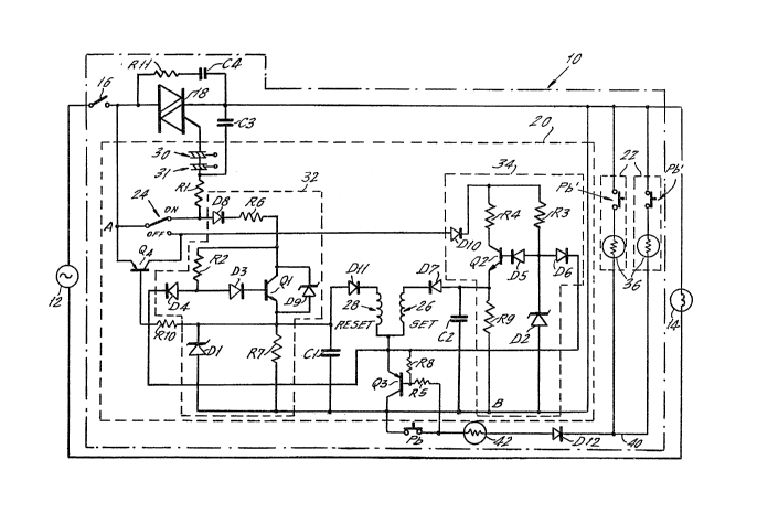
Referring now to Fig. l, there is illustrated a
presently preferred embodiment of a load control system
constructed~in accordance with the principles of the
present invention and designated generally as 10. Load
control system 10 is connected between a power source 12
and one or more loads 14. While the load 14 is illus-
trated as being an incandescent lamp, load control system
10 may be used in connection with other loads including
capacitive and inductive loads. To control the applica-
tion of power from source 12 to load 14, control system
10 preferably includes both a manually controlled air gap
switch 16 and a bidirectionally conductive electronic
switching element 18 which is polarity insensitive (each
~88~
-- 7 --
of i~s main terminals can be applied to the source 12 or
load 14 without affecting the operation o~ the elemen~).
The operation of electronic switching element 18 is con-
trolled by a latching control circuit 20 in response to
the receipt o~ a control signal generated by either the
local push button switch Pb or any of the remote switch
units 22. Latching control circuit 20 is also polarity
insensitive and includes a bi-stable latch which switch-
es between the ON and OFF state each time a local push
button switch Pb (preferably located in the same housing
as control circuit 20) or a push bu~ton switch Pb' (lo-
cated at one of the remote switch units 22) is de-
~pressed. In the OFF state, control circuit 20 removes
gate curre~t from electronic switching element 18 (pref-
erably a triac) thereby removing power from load 14. In
the ON state, control circuit 20 ~ires triac 18 shortly
after each zero crossing o~ the AC wave form Vs (Fig. 2)
generated by source 12 with the result that a substan-
tially si~usoidal wave form is applied to load 14.
The control circuit 20 and associated push button
switch Pb are preferably located in a single housing adapted
to be installed in a standard wall box. One such housing is
illustrated in Figures 11-14 of applicants U.S. Patent No.
4,543,592. This housing incorporates a short-throw, light-
force push button switch which has a highly pleasing tactile
feel and needs only be depressed a short distance to move it
from its normally open to its momentarily closed position.
While the present invention is not limited to the use of such
a switch (other mechanical, touch plate, beam break and
remote control switches may be used), the use of a short-
%
~2~?3871
throw, light force switch is preferred. Such a switchmay be used with the present invention because-the push
button switches Pb, Pb' are subject to low magnitude
control voltages and not full line voltages and load
currents. ~ppliCQ~ V S ~x~e~t ~,~,5~3~57
~ n theA
only the push button switch is located in the remote
housing. When the structure of Figures 11-14 of the
foregoing application is used in connection with control
circuit 20 of the present invention, the control circuit
20, as well as the triac 18 and air gap switch 16, are
all preferably located within the single housing. The
air gap switch 16 is manually controlled by the operator
of system 10, for example by a toggle switch located in
the lower right hand corner of the face plate.
Each of the remote switching units 22 includes
a push but~on switch Pb' in series with a positive tem-
perature coefficient resistor 36 which protects the push
button switch Pb' from high currents in the event that
the remote switching unit 22 is improperly wired. As
with the main control unit, each remote switch unit 22
pre~erably takes the form illustrated in Figures 11-14 of
applicants U.S. Patent No. 4,543,592. These wall plate units
are located at locations remote from control circuit 20
and send a control signal to control circuit 20 whenever
one of the push button switches Pb' is depressed. This
low voltage control signal causes the latching control
circuit 20 to toggle from its present state (e.g. the ON
state) to the opposite state (e.g. the OFF state).
Latching control circuit 20 can be either an
electronic, electromagnetic, or mechanical bistable
X
~2~ 37~
latching circuit. In the presently preferred embodi-
ment, an electromagnetic latching circuit is used. The
heart of latching control circuit 20 is a latching relay
comprising a bi-stable contact 24, a set coil 26 and a
reset coil 28. Whenever current is pulsed through set
coil 26, contact 24 switches to the ON position. Whenev-
er current is pulsed through the reset coil 28, contact
24 switches to the OFF position. The contact 24 is main-
tained in the ON and OFF positions by permanent magnets.
The position of contact 24 defines the state of operation
of the latching control circuit 20 and thereby the mode
of operation of triac 18. When contact 24 is in the ON
position, control circuit 20 gates triac 18 shortly af-
ter zero crossing of each half cycle of the AC wave form
Vs of source 12 with the result that a substantially
sinusoidal voltage Vl (Fig. 2) is applied to load 14.
When contact 24 is in the OFF position, gate current is
removed from triac 18 and the triac is cut off thereby
removing power from load 14.
The operation of control circuit 20, and
thereby the operation of triac 18, is varied as a func-
tion of the position of relay 24. Relay 24 is toggled
from the ON to the OFF position whenever capacitor Cl
discharges through the reset coil 28 and toggles from the
OFF to the ON position whenever capacitor C2 discharges
through set coil 26. The charging of capacitors Cl and
C2 is controlled by reset capacitor charging circuit 32
and set capacitor charging circuit 34, respectively. The
discharging of capacitors Cl, C2 is controlled by tran-
sistor Q3 which is turned on by the control signals ap-
plied to its base by local push button switch Pb and/or
.
' ', ", :
, :.
~L2~ 7~
-- 10 --
remote control circuits 22. The operation of reset ca-
pacitor charging circuit 32 will be described first.
When contact 24 is in the ON position, the
voltage at node A will attempt to follow the source volt-
age Vs . This sine wave is illustrated in Figure 2.
Node A (Fig~ 1) is coupled to the gate of triac 18 via
contact 24, resistor Rl and silicon bilateral switches
30, 31 (any suitable bilateral break over device can be
used). The silicon bilateral switches 30, 31 are de-
signed to break over whenever the magnitude of the volt-
age across the switch exceeds a predetermined level. The
magnitude of the break over voltage is chosen to be suf-
ficiently small to ensure that the voltage applied to
load 14 is substantially a sinusoidal voltage while at
the same time sufficiently large to provide charging
current to capacitor Cl. A break over voltage o~ approx-
imately 15 volts has been found to be suitable. This
provides for a off time of approximately one hundred
microseconds for the triac 18 yet provides sufficient
charging voltage to capacitor Cl. As a result of the
silicon bilateral switches 30, 31, the voltage Vg be-
tween nodes A and B will be a pulsed voltage having a
short duration and having a maximum value equal to the
level to which capacitor Cl is to be charged. This volt-
age Vg is illustrated in Figure 2.
While the maximum value of Vg is set to be
equal to the desired maximum voltage level to which ca-
pacitor Cl charges, the duration of the Vg pulse is very
short (preferably no more than about 5% of one half cycle
of the AC wave form Vs). The use oE such a short pulse
is required to ens~re that the load voltage applied by
871
triac 18 will be substantially sinusoidal thereby permitting
th~ system 10 to control capacitive loads. The shor~ off
time also serves to minimise incidental radio frequency
interference, acoustic noise which may be generated by lamp
or transformer loads controlled by the system, and inrush
current stresses in the switching device. While such a short
pulse duration is desirable in terms of the wave form applied
to the load, it provides a very brief time period during
which source 12 can supply power to control circuit 20. The
design of control circuit 20 makes this possible by requiring
a very small amount of power--the power required to maintain
sufficient charge on either the capacitor Cl or C2 (depending
upon the position of contact 24) at a level sufficient to
drive the reset and set coils 28, 26, respectively.
It is desirable to charge the reset capacitor Cl quickly
since the operator of system 10 has to wait until capacitor
Cl charges before the system can be switched to the OFF
state. In order to ensure that capacitor Cl can be charged
to the required value in a short period of time (typically
100 to 200 milliseconds), it is necessary that the resistor
R6 through which the charging current to capacitor Cl flows
have a low value. The use of such a resistor could, however,
create problems once capacitor Cl has charged to the desired
level. Since capacitor Cl will charge in such a short period
of time due to the use of the low value resistor R6, it is
quite possible, indeed likely, that the operator of system 10
will still be depressing one of the push button switches Pb,
Pb' after the capacitor Cl has charged to its maximum value
(determined by zener diode Dl). Since the push button switch
Pb, Pb' is still closed, transistor Q3 will be on and current
would be permitted to flow directly through resistor R6 into
the reset coil 28 thereby inadvertently toggling the control
~88~91
circuit 20 back into the OFF position. To avoid this
problem, reset capacitor charging circuit 32 includes the
transistor Ql which acts as a current regulator. Whenever Q3
is off (this will occur whenever push buttons Pb, Pb' are all
open) and relay contact 24 is in the ON position, transistor
Ql allows current to flow into capacitor Cl. Whenever
transistor Q3 is on (this will occur whenever any one of the
push button switches Pb, Pb' is closed), transistor Ql will
be cut-off (this is described in greater detail below) and
will prevent current from flowing directly to the reset coil
28.
Once the operator of system lO has released the push button
switch Pb, Pb' he had originally depressed and capacitor Cl
has charged he can switch control circuit 20 to the OFF mode
by depressing any of the push button switches Pb, Pb'.
Whenever any of these switches are closed, base drive (the
control signal to control circuit 10) will be available to
transistor Q3 and the transistor will turn on. This provides
a discharge path for the voltage across capacitor Cl through
reset coil 28, diode Dll and transistor Q3. The current
pulse passing through reset coil 28 causes the contact 24 to
switch to the OFF position. This cuts off triac 18 and once
the push button switches Pb, Pb' have been released initiates
tha charging of capacitor C2.
In the OFF state, the entire supply voltage Vs is available
across nodes A and B. As soon as the push button switch Pb,
Pb' which initiated the transfer of operation of the latching
control circuit 20 from the ON to the OFF mode has been
released, transistor Q2 will turn ON and charging current
will flow through the diode
X
37~L
- 13 -
D10, the resistor R4 and the transistor Q2 to the capaci-
tor C2. If capacitor C2 were permitted to charge to the
full source voltage, the current which would pulse
through set coil 26 when one of the push buttons switches
Pb, Pb' was subsequently depressed could destroy the
coil. To avoid this problem, a Zener diode D2 is placed
in series with a diode D5 between node B and the base of
transistor Q2. As soon as the voltage across capacitor
C2 reaches the break over level of Zener diode D2, tran-
sistor Q2 will turn OFF and the current flow to capaci-
tor C2 will cease. At this time, capacitor C2 will be
free to discharge through diode D7, set coil 26 and tran-
sistor Q3 the next time one of the push button switches
Pb, Pb' is depressed.
When control circuit 20 is in the OFF mode,
triac 18 is OFF and current flow to load 14 is stopped.
In this mode, it is extremely important that the leakage
current through the control circuit 20 be minimized. The
transistor Q2 carefully regulates the flow of current
during the OFF mode of control circuit 20 to prevent any
significant leakage current. As soon as the push button
switch Pb, Pb' which initiated the transfer o~ operation
of the latching control circuit 20 from the ON to the OFF
mode has been released transistor Q2 turns ON and sup-
plies current to capacitor C2 via diode D10 and resistor
R4. Since this current is being used to charge capacitor
C2, there will be some leakage current. Once capacitor
C2 has charged to the voltage driven by diode D2, tran-
sistor Q2 shuts off but current continues to flow through
diode D10, resistor R3 and Zener diode D2. The reverse
leakage current through Zener diode D2 is relatively
-
. "
.
1~8~
- 14 -
small and is reduced even further by the high value re-
sistor R3 (e.g. 560K ohm). If an attempt was made to
reduce leakage current by using a high resistance for
resistor R4 and omitting transistor Q2, the charging
time of capacitor C2 would be extremely slow (as long as
one second). This would be highly undesirable since it
would prevent the latching control circuit 20 from being
switched back to the ON condition for a period of at
least one second. By steering the current in the manner
described above, the transistor Q2 avoids this problem.
As discussed above, transistor Ql ensures that
current will not flow from the source 12 to the reset
coil 28 while a push button switch Pb, Pb' is depressed
(i.e. while the control signal is being applied to con-
trol circuit 20). The transistor Q2 which forms part of
the set coil charging circuit 34 serves a similar pur-
pose.
Assuming that contact 24 is initially in the
ON position and push button switch Pb is depressed, ca-
pacitor Cl will discharge through Dll, reset coil 28 and
transistor Q3 causing contact 24 to switch to the OFF
position. If transistor Q2 were permitted to be on at
this time (or if the transistor were omitted) charging
current could immediately flow from source 12 to capaci-
tor C2. While this would be acceptable, a significant
problem could occur once capacitor C2 had accumulated a
significant amount of charge~ As the voltage across the
capacitor C2 increases, so does the voltage available to
energize set coil 26. If the push button switch Pb con-
tinues to be depressed, transistor Q3 will be on and
current will be free to flow through coil 26. IE this is
38~1
15 -
permitted to occur it will cause contact 24 to return to
the ON position. The process can repeat itself as long
as switch Pb is closed and a toggle situation can occur.
To avoid this problem, the base of transistors
Ql, Q2 are coupled to the emitter of transistor Q3 via
respective diodes D4, D6. Whenever a push button switch
Pb, Pb' is depressed, transistor Q3 removes base drive
from transistors Ql and Q2 via D4 and D6 thereby turning the
transistors off. This disables charging circuits 32, 34
during the period that any of the push button switches Pb,
Pb' are depressed and prevents current ~rom source 12
from passing through coils 26, 28. While this also de-
lays the charging of capacitor Cl, C2, this is acceptable
since the appropriate capacitor will be charged very
quickly when the push button Pb, Pb' is released due to
the current regulating characteristics of the transis-
tors ~1, Q2.
Summarizing the foregoing, the interaction of
contact 24, low value resistors R6, R4, and transistors
Ql-Q3 ensures that the appropriate capacitor Cl, C2 is
charged only after the push button switch Pb, Pb' which
had been closed is returned to the open position (so that
the coils 26, 28 cannot accidentally be energized) and
that the capacitors Cl, C2 are quickly charged when the
push button switch Pb, Pb' is released (to ensure that
the system can intentionally be switched between the OFF
and the ON mode very quickly).
While the above described structure ensures
that the capacitors Cl, C2 are charged very quickly (e.g.
in 100 milliseconds), it is possible that two push but-
ton switches Pb, Pb' will be successively closed in such
X
i81~
- 16 -
a short time interval that the charge in the appropriate
capacitor Cl, C2 would not reach a sufficient level to
fully energize its associated coil 26, 28. In such a
case, it is possible that the contact 24 would be stuck
between the ON and OFF positions (i.e. the contact would
be in an intermediate position between the ON terminal
and the OFF terminal). In this event, charging current
will not be available to either capacitor Cl or capaci-
tor C2 with the result that the switching system would be
effectively stuck in the OFF condition.
In order to avoid this problem, control circuit
20 includes a bootstrap circuit including transistor Q4,
for automatically charging capacitor C2 in the event that
relay contact 2~ is stuck between the ON and OFF posi-
tions. One of the push buttons Pb, Pb' can then be
depressed to discharge capacitor C2 through set coil 26
and thereby move relay contact 24 to the OW position.
When contact 24 is stuck between the ON and OFF
positions, transistor Q4's base drive current path is
from node A into the emitter of transistor Q4, out the
base of transistor Q4, through Rl0 and R7. Note that
node A is on the opposite side of triac 18 from the lower
end of R7. It is the voltage across triac 18 which
provides the drive for transistor Q4's base current.
Transistor Q4 can receive base drive whenever Vs > VCl
(the voltage across Cl). It is not necessary for VCl = 0
for transistor Q4 to turn on. Thus whenever transistor
Q4 has base drive and Vs > VC2 (the voltage across C2),
transistor Q4 will turn on and charge C2 up to a voltage
limited by Zener diode D2 (e.g., 18V). Resistors R10 and
R7 are
~Z~81~7~
- 17 -
chosen such that when transistor Q4 is on, C2 will charge
fully in less than one second which sho~ld be unnotice-
able to the user.
The last part of the bootstrap circuit is
resistor R9 which functions purely as bleeder resistor.
The value of resistor R9 is chosen such that any leakage
or noise current through transistor Q4 when it should be
off will not charge capacitor C2 but will pass through
resistor R9. Resistor R9 is also large enough that it
will not significantly discharge capacitor C2 under nor-
mal conditions.
In order to protect control circuit 20 from
excess voltages due to improper wiring of the control
circuit during installation of switching system 10, a
positive temperature coefficient resistor 42 is placed in
series with Diode D12 in the control line 40. The diode
D12 makes it possible to have a single remote switch
coupled to a plurality of load control systems, each
controlling the operation of different sets of loads, and
to have that single remote switch operate as a control
switch for each of the control systems. This is
described in greater detail in application Serial No.
541,368 except that in the foregoing application the
diodes are external to the control circuitsO
A snubber circuit comprising resistor Rll and
capacitor C4 are placed in parallel with triac 18 to
limit the rate of rise of voltage across the triac so as
to protect the same when it is used in connection with
inductive loads.
Under normal conditions, the charging voltage
to capacitor Cl is the low duty cycle pulsed voltage Vg
illustrated in Figure 2. This voltage is typically no
gLZ~ 71
- 18 -
~ore than 15 volts. In the event that the contact 24 is
toggled from the OFF to the ON position at some point other
than the voltage zero crossing of the AC source 12, a
relatively large voltage could appear between nodes A and B
before triac 18 is fired. To protect the transistor Ql in
the event of such a large voltage, a Zener diode D9 is placed
parallel with the coll~ctor and emitter of transistor Ql.
As noted above, the switching system 10 is
designed for inductive as welL as resistive loads. When
used with an inductive load, the current lags the voltage
as shown in Figure 3. Referring to Fig~ 3, the current
goes to zero at time t and the triac 18 turns OFF. The
triac 18 needs a gate pulse to begin conducting in the
opposite directionO The voltage available across the
triac 18 depends on how inductive the load is but can
easily be as high as 130V. This ~ould cause the gate to
fire instantaneously which would provide no time to
charge capacitor Cl. To avoid this problem, a capacitor
C3 is placed in parallel.with the series connection con-
sisting of the silicon bilateral switches 30 and 31 and
the gate of triac 18, and delays the instant at which
triac 18 turns ON by a short.period of time sufficient to
allow capacitor Cl to charge but short enough to pre-
serve the desired essentially sinusoidal wave form ap- -
plied to load 14.
While the capacitor C3 ensu~es that capacitor
Cl will charge even with highly inductive loads, the
delayed firing of triac 18 results in voLtages across
nodes A and B of greater than the 15 volts to which the
capacitor Cl is designed to be charged. For this reason,
X
12~ 7~
- 19 -
a Zener diode Dl is placed in parallel with capacitor Cl
to limit the charge on capacitor Cl to safe le~lel~.
The presently preferred values of the
resistors, capacitors and Zener diodes of Figure 1 is set
forth in table 1 below.
TABLE 1
VALUE VALUE IN VALUE
RESISTOR IN OHMS CAPACITOR MICRO FARADS ZENER IN VOLTS
Rl 150 Cl 68 Dl 22
R2 22k C2 68 D2 18
R3560k C3 0.22 D9 22
R4 2.2k C40.0~7
R5 3.3k
R6 47
R73~0k
R8 47k
R9390k
R10 1.2M
Rll 1~
All diodes are type lN4004. Triac 18 is an MAC224-5.
Transistor Ql is an MPS-A13, transistor Q2 is a 2N6517,
transistor Q3 is an MPS-A56 and transistor Q4 is an MPS-
A92.
The load contral system lO of the foregoing
embodiments has several advantages. Because the only power
needed for the control circuit 20 is the power required to
charge and maintain the charge on the capacitors Cl and C2,
the triac 18 can remain on for substantially the full AC wave
form. This makes it possible to utilize the control system
10 with capacitive loads. The time required to charge the
capacitor Cl and C2 to the
37~
- 20 -
required level can be very short due to the use of the
low value charging resistors R6 and R4. These resistors
can be used due to the operation of the capacitor charg-
ing circuits 32, 34 which make it possible to use low
charging resistors while at the same time preventing
high leakage currents and the possibility that the con-
tact 24 would go into a ~oggle state while the push
button switch Pb is depressed.
Another ~ajor advantage of the present
invention is the control circuit 20 is powered by the
voltage across triac 18 (both in the ON and OFF condition
of control circuit 20) alone. As a result, the control
circuit need only be connected between the source 12 and
the load 14 and does not have to be connected to neu-
tral.
Another significant advantage of the present
invention is that it is polarity insensitive; the nodes A
and B can be connected to the source 12 and load 14,
respectivPly, or to the load 14 and source 12, respec-
tively.
Another major advantage of the present
invention is that it inherently contains a power off
memory in which the control circuit 20 remembers whether
it was in the ON or the OFF state when power is removed
from the control circuit 20. When the power is returned,
the control circuit will either enable or disable the
triac 18 as determined by the original condition of the
control circuit. The power off memory function is
achieved,as a result of the use of the bistable latch.
If an electronic latch was used for this purpose, a
lithium battery or similar power source would be supplied
.: , .
371
- 21 -
to maintain the latch in its original position before the
AC power to control circuit 20 was removed.
Figure 4 is a schematic diagram illustrating
the manner in which two load control systems 10-1, 10-2
constructed in accordance with the present invention can
share remote control switches. The first control system
lO-l includes a main housing 38 (which houses a triac 18,
a control circuit 20 and the local push button switch Pb)
and three remote control switch housings 42, 44 and 46
(the housings 44 and 46 also forming part of the control
system 10-2 as described below). The housing 42 is
substantially identical in external appearance to hous-
ing 38 and houses a single remote switching circuit 22
including the push button switch Pb'. The housings 44,
46 are also substantially identical in appearance to the
housing 38 except that they each include a pair of remote
control switching circuits 22, each of which includes a
respective push button switch Pb'-l, Pb'-2. The combined
size and shape of the push button switches Pb'-l and Pb'-
2 are approximately equal to the, overall size and shape
of the single push but~on switch Pb' in main housing 38.
The push button switch Pb'-l in each of the housings 44,
46 is coupled to the control circuit 20 of main housing
38 and applies a control signal to control circuit 20
whenever depressed.
The push button switches Pb'-2 of housings 44
and 46 are coupled to the main housing 40 of the load
control system 10-2. Like housing 38, the main housing
40 houses the control circuit 20, the triac 18 and the
push button Pb of the load co'ntrol circuit 10-2. Whenev-
er one of the push button switches Pb'-2 is depressed, it
7l
- 22 -
applies a control signal to the control circuit 20 locat-
ed in housing 40. AS such, the single housing 44 (as
well as the single housing ~6), includes a pair of push
butto.n switches, one for each of the load control systems
10-1, 10-2 and thereby makes it possible to control two
sets of loads from a single remote locatlon.
In the embodiment illustrated, the load control
system 10-2 also includes a housing ~8 which houses a
single remote switching unit 22 including the push button
switch Pb'. While each load control system 10-1, 10-2 is
sh.own as having three remote units, two of which are
located in the same housing as the remote unit for the
other load control system, ~he invention is not so limit-
ed and other combinations can be used.
In the foregoing description of Figure 4, the
control plates at the front of each of the housings 38-46 are
referred to as push button switches. In fact, each push
button switch i5 located internally of the housing and the
element viewed from the front of the housing is an actuator
plate coupled to the push button switch. This is described
in more detail in parent application Serial No. 541,368. As
used in the appended claims, the term "actuator plate" refers
to the plate labeled Pb, Pb', Pb'-l and Pb'-2 in Figure 4.
In the foregoing description, the
bidirectionally conductive switching element 18 is shown
as à triac. Other bidirectional devices can be used.
Additionally, hybrid circuits which effectively operate
as a bidirectionally conductive switching means (e.gD a
pair of back to back SCR's) can also be used.
X
.,': ,, .
'''' ' ' ' ~'.
7~
- 23 -
The present invention may be embodied in other.
specific forms without departing from the spirit or es-
sential attributes thereof and, accordingly, reference
should be made to the appended claims, rather than to the
foregoing specification, as indicating the scope of the
invention.