Note: Descriptions are shown in the official language in which they were submitted.
~:~73
Descri~tion
Microelectrochemical Sensor And Sensor Array
Inventors: Marc J. Madou
Takaaki Otagawa
Technical Field
The present invention relates to micro-
electrochemical sensors useful for detecting various
chemicals, including vaporous and gaseous species and
dissolved species, in very low concentrations. The
micro-electrochemical sensors themselves are
formulated by integrated circuit tIC) engineering
techniques and can be extremely small in size,
namely, as small as one-fifth to one-sixth the size
of the smallest previously known sensors. Among
numerous other uses, they may be utilized to analyze
blood chemistry, in vivo.
Back~_ound Art
In a large number of situations it is
desirable to be able to analyze a sample, be it a
liquid sample or a gaseous sample, ~or one or more
constituents. Often, it is desirable to analyze for
^~
-- ~29887:~
several constituents at once. For example, it is
desirable to be able to analyze blood for such
diverse components as H , K , CO2 and 2' etc. It is
also often desirable to be able to analyze air
samples for air borne contaminants such as CO, NO,
NO2, N2O, SO2, H2S and 2 and other gases as well.
Within the last several years a number of
sensors have been developed based upon one or more
of the techniques developed by integrated circuit
engineering technology. For example, U.5. Patent
4,020,830, issued May 3, 1977 to C.C. ~ohnson, et al,
utilizes a chemical sensitive field-effect transistor
(FET) transducer for selectively detecting and
measuring chemical properties of substances to which
the transducer is exposed. Basically, the chemical
being detected interacts with certain substances to
modulate the electric field produced in the sub~trate
semiconductor material between diffusion regions
thereof. Such FET devices have been demonstrated to
be useable for detecting ions as well as gases, and
indirectly certain dissolved molecules. However,
fluctuations in drain current leading to errors are
still a significant problem. These fluctuations can
be associated with thermal noise or they can be light
induced. Layers that make the FET chemically
sensitive and selective are very difficult to deposit
on the gates of such devices, especially since often
several layers of different composition are needed.
All of this leads to errors or makes fabrication
difficult. Still further, reference electrodes are
very difficult to implement in FET structures.
S.J. Pace, as set forth in U.S. Patent
4, 225, 410, dlscloses a disposable integrsted
\
':
, ~ .
.
- 129~3~73
miniaturized array of chemical sensors for analyzing
concurrently a number of analytes in a fluid sample.
Each sensor of the array is a complete electro-
chemical cell having its own reference and indicator
electrodes and is selective with respect to a
particular analyte. The sensors are all formed on
top of the surface of a substrate which is prepared
by press forming powdered alumina ~ith appropriate
through holes and imprints for the electrochemical
circuit. Because of the manufacturing techniques
such sensors and sensor arrays must be relatively
large and are more properly describable as
minisensors rather than microsensors.
In U.S. Patent 4,549,951, issued october
29, 1985 to M.B. Knudson, et al, a relatively large,
compared to both of the devices discussed above, ion
selective electrode is set forth which is used along
with a separate reference electrode. The ion-
selective membrane of the electrode sits on a
conductor embedded in a plastic substrate, This is
basically a small ion-selective electrode with the
membrane sitting on top of a conductor and without an
internal reference electrolyte or true reference
electrode. Further, construction of such an
electrode design in micro sizes appears to be beyond
the current state of the art.
In the devices of U.S. Patents 4,020,830,
4,225,410, and 4,549,951 the entire electrochemical
cell sits upon the surface of a substrate. This
leads to a significant problem in providing proper
encapsulation. In the case of U.S. Patent 4,020,830,
all of the electronic circuitry is included on the
analyte detecting side of the FET. This leads to
i
i
1298~373
-- 4
problems between the chemicals and the electronic
circuitry which are either in contact ~ith one
another or closely adjacent to one another.
The prior art, including the above
discussed patents, does not yet provide microelectro-
chemical sensors and sensor arrays incorporating both
amperometric and potentiometric elements, which
operate at room temperature and consume little power,
which provide versatile, multi-purpose-multi-channel,
real time monitoring of vapors, gases, molecules
and ions, which are micro-portable and field rugged,
which have fast response times at ambient
temperature, which are free of interferences from
such parameters as oxygen deficiency and humidity,
which can be produced inexpensively using
sophisticated modern micro-fabrication technologies,
which have high specificity and high selectivity, for
example, parts-per-billion level detection of such
' 2~ H2S, SO2, and N2H4 and parts-per-
million detection of such gases as HCN, C12, ~2' 2'
2 5 , 3 3N, 03, C2H2, C2H4~ CH4~ C2H6' C H
and organophosphate vapors, and which are adaptable
for detecting ionic electroactive species in
parts-per-billion in solutions, including, for
example, Cl , Br , I , SCN , CN , S2032 , OCl ,
S032 , phenols, aromatic amines, nitro compounds,
organoarsines, and metal ions, e.g., Cu2 , Fe3 .
The present invention is directed to
solving one or more of the problems as set forth
above.
'- ~2g~73
Disclosure Of Invention
In one embodiment of the present invention
a microelectrochemical electrode structure is set
forth. The aforementioned electrode structure
comprises a monolithic substrate having a front
surface and a back surface facing generally away from
one another. A first well extends into the substrate
from the front surface towards the back surface and
ends in a first well bottom. A first passage extends
into the substrate from the back surface to the first
well bottom. A first electrolytic cell including a
first electrode is located wholly between the front
and back surfaces of the substrate. A first
conductor is located in the first passage and
electrically communicates the first electrode to
adjacent the back surface.
In accordance with one embodiment of the
invention an electrolytic medium is in the first
well. A barrier covers the first well, the barrier
having an outfacing surface and an infacing surface.
The infacing surface is in flow contact with the
electrolytic medium. The barrier provides entry into
the electrolytic medium of a selected moiety in
response to contact of a selected species with the
outfacing surface. The barrier is at least
substantially impermeable to the electrolytic medium.
Another embodiment of the present invention
is a sensor array including a plurality of such first
electrode structures in the substrate. 1,
Optionally, each electrode structure can
have more than one electrode in the first well.
An electrode structure in accordance with '
the present invention is characterized by extremely
.,
73
small size, is operable at room temperature, utilizes
low power, is field rugged, has a fast response time,
is not sensitive to inter~erences due to oxygen
deficiency or differences in humidi~y, can be readily
mass produc~d using sophis~icated microfabrication
technologies~ has high specificity and high
selectivity, can have very short signal lines to
signal amplification circuitry integrated and
embedded in the back side of the substrate thereby
providing a high signal-to-noise ratio, and is useful
in accordance with specific embodiments to detect
vapors, dissolved ions and dissolved nonionic species
(including dissolved gases). The structure is also
very well suited to having a pressure element
incorporated in an array therewith. Because the
geometric configuration of a resistive or capacitive
sensor is so similar to the structure created for the
chemical sensitive elements it only requires a few
more processing steps to also include a pressure
element on the same substrate. In some applications
(e.g., biomedical) such added features are very
beneficial.
In accordance with embodiments of the
present invention a single substrate can have an
array of one or more electrode structures, each
sensitive for one or several of a number of different
chemical species. And, the entire sensor array can
be so small that it can be readily positioned in, for
example, a catheter in the blood stream and can be
used to give a constant readout of such chemicals as
C2' 2~ K , ~ , and the like. ~n accordance with
certain embodiments of the present invention it is
possible to include integrated circuitry electronics
9.2988S7~
on the back surface of the substrate removed from the
electrochemistry whereby one can amplify the signals
and/or obtain electrical output signals which are
specifically indictive of the concentration of one or
of a number of species. The electrode structure o~
the present invention can be designed to exhibit
substantially Nernstian slopes for ionic species.
The amperometric electrode structures of the present
invention can be designed to exhibit substantially
linear dependency on concentration. The bottom of
the first well can be chosen to be at different
distances from the front and back surfaces of the
substrate for different intended applications.
Brief Description of Drawln~
The invention will be better understood by
reference to the figures of the drawings wherein like
numbers denote like parts throughout and wherein:
Figure 1 illustrates, in a side sectional
view, an em~odiment of a microelectrochemical sensor
in accordance with an embodiment of the present
invention;
Figure 2 illustrates, in similar view, an
alternate embodiment of the present invention;
Figure 3 illustrates, in similar view, an
alternate embodiment of the present invention;
Figure 4 illustrates, in similar view, an
alternate embodiment of the present invention:
Figure 5 illustrates, in similar view; an
alternate embodiment of the present invention;
Fiyure 6 illustrates, in similar view, an
alternate embodiment of the present invention;
,
-` ~2!gi5 ~
Figure 7 illustrates a detail in the
embodiment of Figure 6;
Figure 8 illustrates, in similar view, an
alternate embodiment of the present invention;
Figure g illustrates, in plan view, an
array of microelectrochemical sensors in accordance
with an e~bodiment of the present invention;
Figure 10 illustrates, in plan view, an
alternate array of microelectrochemical sensors in
accordance with an embodiment of the present
invention;
Figure 11 illustrates a side sectional view
of a portion of Figure 10 and shows the combination
of an array of sensor elements with a pressure
sensor
Figure 12 illustrates, in similar view to
Figure 1, an alternate embodiment of the present
invention;
Figure 13 illustrates, in similar view to
Figure 1, an alternate embodiment of the present
invention; and
Figure 14 illustrates, in a side sectional
view, a separate electronics containing member useful
in an alternate embodiment of the present invention.
Best Mode For Carr~ing Out Invention
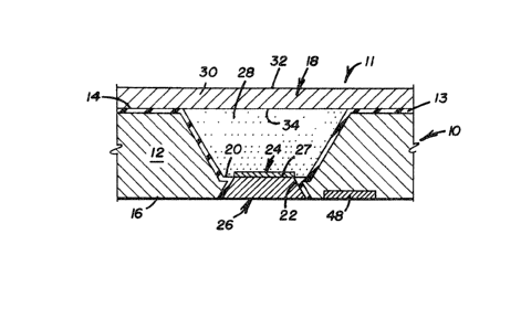
The present invention provides a micro-
electrochemical electrode structure 10 including an
electrolytic cell 11, one embodiment of which is
illustrated in Figure 1. The electrode structure 10
includes a monolithic substrate 12 having a front
surface 14 and a back surface 16 facing generally
away from one another. The substrate 12 can be made
~~ ~L2~a73
of any of a number of materials but it is
particularly advantageous to make the substrate 12
out of a semiconductor material such as silicon,
silicon carbide, gallium arsenide, or the like. The
invention, howev~r, is more general in that the
substrate 12 may also be made of a plastic material,
a refractory oxide, or substantially any other
material. It is even possible to make the substrate
12 of a conductive material, but in such an instance,
and generally in instances in which the substrate 12
is made of a semiconductor material, it is necessary
to provide an appropriate insulating layer 13 to
prevent shorting through the substrate 12. For
example, a silicon dioxide layer 13 can be formed by
contacting a silicon substrate with wet oxygen at
elevated temperature, e.g., about 1000C.
It is important that the substrate 12 be
monolithic i.e., a unitary structure formed of a
single material, as this allows particularly easy
construction and eliminates or greatly reduces
problems of prior art devices. Particular problems
which are eliminated or greatly reduced include:
(1) securing various chemistries to the electrodes
especially when multilayered structures are required;
(2) affixing the membranes that cover the chemistries
in the wells; (3) leakage of electrolyte to the
electronics; (4) the depositing o thick electrolytic
mediums which are sometimes necessary; (5)
encapsulation problems; (6) light sensitivity
problems; (7) lack of versatility to do, for example,
current as well as voltage measurements; (8) high
cost; (9) incompatibilities of various chemistries
with IC processing.
~.2~73
-- 10 --
The electrochemical analysis which can be
made in accordance with the methods of and/or using
the sensors of the present invention includes
voltammetric, potentiometric, coulombic, conducto-
metric and AC analysis.
These problems exist for several reasons.
First, the prior art devices build walls upwardly
from a surface and the build up must be high enough
to contain the chemistry. Second, encapsulation is
difficult since the electronics are at the same
surface as are the chemistries. Third, the gates of
FET devices are exposed to light to which they are
sensitive. Fourth, the electrolyte, being adjacent
the electronics, can leak into the electronics.
Fifth, since the electronics and chemistries are on
the same surface the use of simple bump bonding
techniques to connect sensors with electronics is
precluded.
In accordance with the present invention a
first well 18 extends into the substrate 12 from the
front surface 14 and extends towards the back surface
16. All of the needed chemicals of the cell 11 are
within the first well 18. The first well 18 ~nds in
a first well bottom 20. A first passage 22 extends
into the substrate 12 from the back surface 16 to the
first well bottom 20. The first well 18 can be
formed by any of a number of techniques, including,
particularly, anisotropic etching carried out in
accordance with the techniques of the semiconductor
industry (in which instance the (100) face of the
silicon corresponds to the front surface 14). Such a
process includes such steps as cleaning the substrate
12, applying a photoresist layer, prebaking the
29~8~73
layer, exposing the photoresist, developing the
photoresist, rinsing the substrate 12, drying the
substrate 12, and post baking it. Methods for
carrying out each of such steps are known in the IC
art and descriptions of such techniques may be found
in, for example, "Integrated Circuit Engineering" by
A.B. Glaser and G.E. Subak-Sharpe, Addison-Wesley
Publishing Company, Reading, Massachusettes, 1977.
In this same text are found explanations of etching,
oxidation of silicon, formation of a silicon nitride
insulating layer, and the like.
An alternative way of forming well 18 (and
passage 22 as well) is by laser drilling. Holes of
various forms with lateral extensions from a few
microns to hundreds of microns can be formed by this
method. Depending on the depth, a process time, per
hole formation, of less than 1 second can be
involved. The silicon wet anistropic etching
technique has two major advantages over laser
drilling. One, it is a parallel process whereby many
holes can be made at once. Two, the surfaces are
smooth and very well defined. The advantage of laser
drilling is that it can provide straight but not
smooth walled holes when such are desirable.
In accordance with an embodiment of the
present invention a first electrode 24 is provided
which is, very importantly, wholly between the front
surface 14 and the back surface 16 and which extends
at least to the first well 18. This is very
important as this enables the securing of subsequent
layers in a straight-forward fashion, makes the
accommodation of the electrolytic medium in general
easier (for example, eliminates spilling using an ink
:~,
. .......
1291!it~73
jet printer type of chemistry filling device), and
allows for an easier fixing of additional barriers.
Also better encapsulation is provided.
A first conductor 26 is provided in the
first passage 22 and serves for electrically
communicating the first electrode 24 to adjacent the
back surface 16 of the substrate 12. The first
conductor 26 is suitably an electronic, as opposed to
an ionic, conductor. Alternatively, a well facing
end 27 of the conductor 26 can play the role of the
electrode 24. This feature makes the fabrication of
the sensor 10 dramatically simpler. Often, however,
the sensor electrode metal will need additional
backup layers (e.g./ aluminum or titanium) for
strength and/or economy.
The first passage 22 can be made by any of
the known techniques of the semiconductor art. For
example, such techniques as anisotropic etching,
laser drilling, aluminum thermomigration, and the
like are useful. The first conductor 26 can be
provided in the first passage 22, again by the
techniques of the semiconductor art. For example,
the first conductor 2~ can be provided by such
techniques as aluminum thermomigration, metal
deposition, (evaporation or sputtering), electroless
plating, electron beam evaporation, mechanical
positioning of metal rods, melting in place with
vacuum application~ or the like. ~luminum
thermomigration is a useful technique to make the
metal contacts. This technique has the advantage of
providing the hole and conductor in a single
operation. In practice, however, the thermomigration
technique is quite difficult and wet anistropic
98873
etching followe~ by metal deposition is currently
preferable.
Various types of electrode structures 10
can be formed. These include, for example, the
Ag/AgCl xeference electrode, platinum, platinum
black, silver, gold, iridium, palladium,
palladium/silver, iridum dioxide, platinum
black/paladium, platinum oxide, and mixtures thereof,
electronically conductive polymers, and generally any
of the electrodes normally utilized in
electrochemical measurements. Table 1 sets forth, as
examples only, a short list of gases, and
electrochemical systems which have been used to
determine them.
In certain embodiments of the invention an
electrolytic medium 28 is provided in the first well
18. The electrolytic medium 28 can be a liquid but
more preferably is in the nature of a hydrogel, a
plasticized polymeric membrane for potentiometric
elements, an ion selective membrane, or a solid
polymer electrolyte.
The needed materials for the various
electrode structures 10 can be placed in the
appropriate wells 18 as follows: pure metals if they
need to be deposited from the front can be sputtered
or evaporated, electron-beam or ohmic evaporation may
be used, insoluble deposits of metal salts can be
formed by chemical or electrochemical treatment of
metals in situ. They can be deposited from the back
as previously set forth. For providing the hydrogel
one has the choice of lift off technology or ink-jet
printer like technology. Solid polymeric
electrolytes can be put in place in the same manner
2988~3
as hydrogels. Also, ion-selective membranes can be
placed in the appropriate well(s) in the same manner
as can hydrogels. Further, liquid membranes can be
provided in the same manner. Composite membranes,
which include enzyme based membranes, tissue
cultures, living organisms, anti~en-antibody and
generally biocatalyst materials can also be placed in
the well in the same manner.
In principle, all gases or vapors that can
be electrochemically oxidized or reduced can be
sensed by limiting current measurement using
amperometry. The reactions occur at a characteristic
potential at the electrode/electrolyte interface. An
appropriate potential at which only the desired
reaction proceeds must be applied to the electrode so
as to obtain potential-controlled selectivity.
Selectivity (or the ability to observe only one of
the many possible reactions) can be either kinetic or
thermodynamic in origin. Thus, the selectiv~ty is a
function of the sensing electrode catalyst and
~material) potential.
~ n approximate indication of the suitable
range of potential is provided by the reversible
potentials of the reaction involved; some values are
listed in Table 2. Note that each gas reaction
exhibits a characteristic thermodynamic potential.
An example of thermodynamic selectivity is the
reduction of N02 that occurs at low potentials
(Sedlak and Blurton, 1986).
- 14~ -
~ ~z~ 3
E
v C E~ ~ a~ ,_
.r, o ~ e ~ e .¢ ~ e a. E~ -- e ~ e
~ U ~ ~ ~ ~ D ~ D 2 u~ ~ ~
V ~ ~ ~ ~ ~ ~ ` ~ ~ o
a~ ~ o o o . o ~ o co o D ~
Z Z Z
~ ~ 0 0
~ U~ ~ O U~
v ~ _~ ~ r ~ ,,
~1 O ~ O V _~
E~ ~C 'C '~
~o o ~ o ~ o
~t 2 C~ z Z
~ U~
O X ~ ~., ~ ,,, ~ ~, O O
a~
~0 ~ o ~ o
S
X : ~~ V
_I ~ D N ~ _~N ~V ~ ~ al N ~ --1 N ~
3 t; ~ '^ ~ 0 ~,
aI o ~ o ~:id O ~ 1 tlJ O ~ 10 0
~E ~ O~ ~ ~~.q Ov J~ .q ~ .q O ~ R O
o ~-~ ~*~ u"~-' o~e ~c
o ~ o I o ~ o ~ o .~: o I o ~ I o
~ ~a v ~ ~l ~ 4~ w _1 ~ ~ _1
_I ~ O 0 ~O a~~ 0 h tl) O IL~ 0 Q~
~3 P~ V E~V ~ ~ ~ ~a
m O O ~ O O O O
t~ ~ _ Z Z Z Z ~:
Ll~ o ~ o
-1 4b- ~L291!~8'73
Ul ~ ~
W ~ ~ X ~1
V~ ~ .,
o , ~ ~.
3 3
~- ~D O )- O 1
J o ~ Q ~7
o ~ ~ o c I ~ o
a ~ 3 ~ ~ 3 ~ o a " o
a ~ 0 3 ~ a p,
O ~ Q-
O ~ ~ ~0
n ~ 1-
C ~ ;~ ~ t~ 3 w Q
~ ~ n ~ ~ o o
Q O ~
,_
~ C
C ~ Q ~ ' I O ~ O
1--rt O i-~ ~ CO o ~
C ~ ~
O Ft ~1~ 3 ~ )--
tt~ J i~ N ~--
o ~ z
3 : Q ~~, o ,~
,t
l ~
,_
o _ ~-- ~ ~ _c~
~ Ul O O ~ o o,t
o~ ~ o ~ c~O E~ ~3 3
O _
.. ' `~ . .
38'73
Table 2
Thermodynamic Potentials
Of Reactions Involv ~ ases
Thermodynamic
E
Reaction (mV vs NHE*)
Oxidation reactions:
HCHO + H2O ~ CO2 + 4H + 4e -123
2 2 2H 2e -103
H + 2H+ + 2 ~
C2H5OH + 3H2O ~ 2CO2 + 12H+ + 12~ 87
H2S ) S + 2H + 2e 141
52 + 2H2O ~ SO4 + 4H + 2e 170
~C2N2 + H + e 373
4 2 3 2H + 2e 586
NO + 2H2O ~ NO3 + 4H 3e 957
Reduction reactions:
O3 + 2H + 2e ~ 2 + H2O 2076
Cl2 + 2e ~ 2Cl 1360
2 + 4H + 4e ~ 2H2O 1230
NO2 + H + e ~ HNO2 1093 `~
C2 + 2H + 2e ~ HCOOH -199
~NHE = nor_1 hydrogen electrode
I
i
'
~: :
' . ` ,
,, ' , :
-` ~Z~
- 16 -
Because NO2 is reduced to NO and the N~ product is
not further reduced, the NO2 sensor (with sensing
electrode operated at low potentials) is selective
for NO2, having no signal for the NO that may be
present. This NO2 selectivity results from control
of the sensing electrode's potential in a range such
that no NG reactivity is observed. The potential of
~he electrochemical cell has been compared to the
temperature of a catalyst sur~ace tBlurton and
Stetter, 1977), which also may be used for control of
the catalyst reactivity. Control of the potential is
accomplished in many sensors by using three
electrodes and a potentiostatic circuit.
More exact information as to a suitable
range of potentials is afforded by the kinetics of
the oxidation or reduction reaction, which can be
discussed only in terms of electrocatalysis. Each
electrocatalyst formulation will have unique
properties. The activity of platinum for CO
oxidation has been found to be 103 to 106 times
better than that of gold. This is a good example of
kinetic selectivity. Both reactions occur on both
metals, but one is orders of magnitude more rapid
than the other. Although the presently available
sensors utilize expensive, noble metal catalysts, the
required amount of such a catalyst for each sensing
element in electrode structures 10 in accordance with
the present invention is minimal because the sensor
is a microsize device. Moreover, inexpensive
electrocatalysts based on polymer materials that
exhibit catalytic activity and selectivity as high as
those of noble metals can be used in place of the
noble metals.
~2~8~73
If the gas to be sensed exists in a mixture
containing several reactive components that exhibit
close thermodynamic selectivity potential (cf. Table
2), the concentration of the desired component can be
determined selectivity by the differential pulse
voltammetry (DPV) technique. Let us consider a
simple example where a mix~ure of Gas A and Gas B
exists. Gas ~ and Gas B would exhibit current vs.
potential curves with different limiting currents IA
and I~. By differentiating these curves, one obtains
two sharp clearly separated peaks with different
characteristic potentials, EA and EB. The peak
current values are proportional to the gas
concentrations. Thus, the ~PV technique, in addition
to an improved signal-to-noise ratio, can provide
potential-controlled selectivity to an electro-
chemical sensor through precise measurements of Epeak
values, which are closely related to the thermo-
dynamic potentials given in Table 2 and are
characteristic to each gas species.
Among useful electrolytes, particularly for
amperometric elements are solid electrolytes,
including solid polymeric electrolytes such as Nafion
(a trademark of DuPont) which is part of a class of
solid polymeric ion exchangers which conduct ions
upon exposure to water. Probably the best known
examples are membranes made from polystyrene with
fixed negative sites (sulfonate, carboxylate or
phosphonate) or fixed positive sites (quaternary
ammonium or quaternary phosphonium). Selection as
far as ions are concerned with these materials is
almost exclusively on the basis of charge and for
ions with the same charge discrimination is very
~29~1~373
-- 18 --
slight. For amperometric sensing the use of these
materials is relatively new. Other examples of solid
polymeric electrolytes besides Nafion ~which a is
perfluorinated ionomer) are sulfonated styrene-
divinyl benzene resins and divinyl napthalene
sulfonic acid polymer.
Such polymers are characterized chemically
and physically in that they have a hydrophobic nature
with ionic (hydrophilic) clusters inside. They
conduct ions upon hydration. They exclude co-ions up
to the Donnan failure point at which stage ions of
both types can penetrate into the resin. Neutral
molecules can diffuse readily through such membranes
and especially large organic molecules can dissolve
within the more hydrophobic resins.
Resins can also be used as reference
solutions (see, for example, French patent
publication No. 2,158,905). These ion exchange
resins have been used as the electrolytic medium for
a potentiometric CO2 sensor (see, for example, U.S.
Patent 3,730,86~).
For potentiometric elements membranes can
comprise a polymeric binder or support impregnated
with a solution of an ion selective carrier or
ionophore in a solvent for the ionophore. Membranes
of this type can be tailored to sense particular ions
selectively. For example, for sodium the antibiotic
nonactin can be used as the ionophore in a PVC matrix
plasticized with dioctyl sebaca~e. For potassium,
valinomycine would replace the nonactin.
Useful gels for incorporation within the
sensor structure include, without limitation:
methylcellulose, polyvinyl alcohol, agar,
~29~373
-- 19 --
carboxycellulose, gelatin, agarose, deionized
gelatin, polyacrylamide, polyvinyl pyrrolidone,
hydroxyethylacrylate, hydroxyethylmethacrylate, and
polyacrylic acid. They are characterized in that
they constitute thickened (more viscous) solutions.
They are hydrophilic in natural and include synthetic
polymeric film forming materials.
In certain cases the electrolytic medium 28
can come from a solution being analyzed. In most
cases where the electrolytic medium 28 is present,
however, it is provided during the construction of
the electrode structure 10. Often it will be
undesirable to allow a solution being analyzed to mix
with and/or directly contact the electrolytic medium
28.
A barrier 30, generally in the nature of a
membrane, can cover the first well 18. The barrier
30 has an outfacing surface 32 and an infacing
surface 34 and the infacing surface 34 is in flow
contact with the electrolytic medium 28 so as to
pro~ide a full conductive path. Indeed, the barrier
30 can be at least partially within the first well
18. The barrier 30 provides entry into the
electrolytic medium 28 of a selected moiety in
response to contact of a selected species with the
outfacing surface 32 of the barrier 30. Either the
selected species will pass through the barrier 30 and
will then constitute the selected moiety, or contact
of the selected species with the barrier 30 will lead
to the introduction of a different moiety into the
electrolytic medium 28. The barrier 30 is generally
at least substantially impermeable to the
electrolytic medium 28 to prevent escape and/or
29~a73
- 20 -
mixing with the analyte solution exterior of the
barrier 30. The barrier 30 would not be present, or
would be permeable to a solution being analyzed, in
those instances when the solution constitutes the
electrolytic medium 28.
The barrier 30 may encapsula~e the entire
electrode structure 10 including the front surface 14
and the back surface 16. Alternatively, the barrier
30 may only cover the first well 18, or the first
well 18 and part or all of the front surface 14. It
may be desirable to encapsulate the remainder of the
electrode structure 10, or even all of the electrode
structure 10 including the barrier 30, as a
protection against contamination. Generally, an
inert encapsulating layer (not shown) will serve the
purpose. The encapsulating layer, when present, must
provide access (via, for example, pores or holes
therethrough) to the first well 18 or to the barrier
30 covering the first well 18. It can be formulated
as can the barxier 30.
A number of materials may serve as the
barrier 30. For example, the barrier 30 can comprise
a gas pervious liquid impervious membrane. This is
useful in the situation wherein the sensor is used in
a liquid to detect dissolved gases, for example, if
the electrode structure 10 is utilized in blood.
Other types of materials for utilizing as
the barrier 30 are teflon membranes, silicone rubber
membranes, silicon polycarbonate rubber membranes,
mylar, nylon 6, polyvinyl alcohol, polyvinyl
chloride, methylcellulose, cellulose acetate, high
density polyethylene, polystyrene, natural rubber,
fluorosilicone, dimethylsilicon rubber, any
~298873
- 21 -
appropriately perforate photoresist polymer, and
dimethylsilicon. It is generally preerred that the
membranes utilized be solution castable so as to make
fabrication of the membrane more easily accomplished.
The barrier 30 can be placed over
appropriate of the wells 18 by, for example: solution
casting, separate casting on a different substrate
and physical transfer, heat shrinking in place,
solution casting utilizing an ink-jet printer, spin
coating, or dip coating. If the barrier is in the
nature of uniform latex microspheres, made for
example of polystyrene, styrene-butydiene, or teflon,
such microspheres can be placed in position utilizing
the ink-jet technique, by dipping, by solvent
spraying, or the like. If the barrier is of the
nature of or includes activated carbon or similar
materials it can be placed in position by ink-jet
printing, solvent casting, or the like. If the
barrier includes, for example, permanganate coated
alumina or other substance which serves to remove
nitric oxide, it can be placed in position similarly
to the carbon particles.
The microelectrochemical electrode
structure 10 just describ~d may serve as a working or
sensing electrode, a reference electrode, or a
counter or auxiliary electrode. As may be seen in
Figure 2 a single substrate 12 may have one or more
each of a sensing electrode cell 29, a re~erence
electrode cell 31, and a counter electrode cell 33
thereon with appropriate provision, e.g., salt
bridges 35,37, being made for ionic conductivity
between the various electrode cells, or more
particularly between the ~arious electrolytic mediums
~ ~, ~ .,. .. , , . .. , .i . . ,
~2988''73
28,39,41 contacting the various electrodes. The salt
bridges 35,37 are necessary when barrier 30 is a
barrier for all ions.
Note that the designations S, R and C are
used in the figures to indicate, respectively,
sensing, reference and counter electrodes.
If the first electrode 24 is a sensing
electrode the substrate 12 will also include a
reference electrode 36 in ionic electrical
communication with the first electrode 24. The
reference electrode 36 will also be electrically
isolated from the sensing electrode 24 other than via
the electrolytic medium 28. For example, if the
substrate is silicon an appropriate silicon dioxide
or silicon nitride layer 13 can be conventionally
deposited or formed in the first well 18 and in the
first passage 22. The reference electrode 36 can
also be provided with its own different electrolytic
medium 39 (Figure 2) containing the species which
determine the reference electrode potential. Also,
the counter electrode 42 can be provided with a
separate electrolytic medium 41 (Figure 2).
In the embodiment illustrated in Figures 3
and 4 the sensing electrode 24 and the refer2nce
electrode 36 are each in the first well 18. In such
an instance the substrate 12 has a second passage 38
extending from the back surface 16 of the substrate
12 to the reference electrode 36 in the first or
sensor well bottom 20. A second conductor 40 is in
the second passage 38 and serves for electrically
communicating the reference electrode 36 to adjacent
the back surface 16 of the substrate 12. If the
substrate is silicon the silicon dioxide or silicon
1298873
nitride layer 13 also extends along the second
passage 38.
A counter electrode 42 is provided in those
instances when such is necessary, for example, for
ma~ing non-potiometric measurements. The counter
electrode 42 (see Figure 3) is in ionic electrical
communication with the electrolytic medium 28 and is
electrically isolated from the sensing electrode 24,
and from the reference electrode 36 (when such is
present), other than via the electrolytic medium 28.
The counter electrode 42 may be in the same well 18
as is the sensing electrode 24, as illustrated, for
example, in the embodiments of Figures 3 and 4. And,
the counter electrode 42 can, be in the same well as
is the reference electrode 36 as in the embodiment of
Figure 3. The counter electrode 42 may be in the
same well 18 as is the sensing electrode 24, that is
it may be in the first well 18. This embodiment is
seen in Figures 3, 4, 11, 12 and 13.
In the structure of Figure 3 the substrate
12 has a third passage 44 extending from the back
surface 16 thereof to the first well bottom 20. A
third conductor 46 is located in the third passage 44
and electronically communicates the counter electrode
42 to adjacent the back surface 16 of the substrate
12.
In the case of Figure 4 the counter
electrode 42 also plays the role of reference
electrode 40. The silicon dioxide or silicon nitride
layer 13 provides needed insulation.
In certain instances, for example, AC
measurements, conductometric measurements, and the
like, it may be desirable to have more than three
8~3~73
- 24 -
electrodes in a single well 18. Figure 5 illustrates
such a structure.
In a particular instance (not shown) the
well 18 can be in the nature of a trench in which
electrophoresis is carried out by providing a
potential gradient along the length of the trench.
Appropriate sensing electrodes 24 are speaced along
the bottom of the trench whereby various species can
be determined. Appropriate reference 36 and/or
counter electrodes 42 are also provided along the
bottom of the trench.
Electronic circuitry 48 can advantageously
be included in certain embodiments of the present
invention in the substrate 12 adjacent the back
surface 16 thereof. Such electronic circuitry 48 is
adapted for, and serves for, processing signals from
one or more of the sensing electrode 24, the
reference electrode 36, and the counter electrode 42.
The electronic circuitry 48 can be formulated by
conventional integrated circuit fabrication
techniques. Generally the circuitry will serve to
convert the signals from high impedance to low
impedance and may also amplify the signals from the
electrodes, and, if desired, perform computational
tasks and present the data in condition for display
or printing out, for example as concentrations of the
species being detected. The length(s) of the
conductor(s) 26,40 and/or 46 in such instances can be
kept extremely short leading to a very high
signal-to-noise ratio and, therefore, increased
sensitivity. Note also that the chemistry in the
first well 18 is completely isolated from the
. . ~ .,
8873
- 25 -
electronic circuitry 48 whereby the integrity of the
latter is protected.
As an alternative to having the electronic
circuitry 48 on the back surface of the substrate 12,
the electronic circuitry 48 can instead be on a
separate semiconductor substrate 50 (see Figure 6)
which abuts the back surface 16 of the substrate 12.
This provides encapsulation and protection of the
electronic circuitry 48.
Figure 7 is an enlarged view of a portion
of Figure 6. It illustrates the use of a bump
bonding techniques to make the needed electrical
connection between the conductor (26,20 and/or 46)
and the electronic circuitr~ 48. The bump bonding
site 52 is spaced from the electrode (24,36 and/or
42) whereby the contents of the cells (29,31,33) are
not damaged by heat during bump bonding. Also, this
allows good bump bonding contact to be made whereby
the resulting bond has good mechanical strength.
Basically, the bump bonding is carried out by
pressing the bumps 54,56 together and heating the
substrate 50. The bumps 54,56 can be of very
different thickness. Good results have been obtained
with the bump 54 of silver and about 2000 Angstroms
thisck and with bump 56 of copper and about 10
microns thick.
Figure 7 also illustrates the technique of
providing the first electrode 24 by depositing a
small amount of an electrode material, e.g.,
platinum, silver, etc., followed by depositing the
first conductor 26,40,46. In such an instance the
first electrode 24 forms a portion of the bottom 20
of the first well 18. Also illustrated is filling in
-` ~298~373
- 2~ -
the passage 22,38 or 44 with a support material,
e.g., a polymer such as a polyimide.
In accordance with one embodiment of the
present invention, ~or example, as illustrated in
Figure 8, the re~erence elec~rode 36 is of the nature
described above. The working or sensing electrode
structure 24, on the other hand, is in the nature of
an ion-selective membrane 58 (as described
previously) covering a sensing electrode base 60
which is attached to a sensing conductor 62 in a
passage 64 which leads from a bottom 66 of the
sensing electrode well 18 to the back surface 16 of
the substrate 12. The analyte medium makes the
electrolytic contact between the ion-selective
membrane 58 and the reference electrode 36. In this
instance the barrier 30 is ion transparent or can be
omitted. Note that the electrolytic medium 39 is not
the same material as is the ion-selective membrane
58.
Any of a number of ion selective membranes
58 can be used. For example, such membranes are
disclosed by M.A. Arnold and R.L Solsky Anal. Chem.
1986, 58, 84R - 101R, M.E. Meyerhoff and Y.M.
Fratecelli, Anal. Chem. 1982, 54, 27R - 44R, M.A.
Arnold and M.E. Meyerhoff, Anal. Chem. 1984, 20R -
48R, and J. Koryta, Analytica Chimica Acta, 159,
984, 1-46.
It is anticipated that in accordance with
the present invention an array of sensing cells can
be provided with occasional reference cells 36. One
such array is illustrated in Figure 9. In the
particular configuration shown in Figure 9 each
reference cell 31 is surrounded by, and can serve as
~29~3873
- 27 -
the reference cell 31 for, several different sensing
cells 29.
It is also contemplated in accordance with
the present invention that on any substrate 12 more
than one sensing cell 29 can be utilized for each
chemical species being analyzed. That is, there can
be two or five, or ten, or any desired number of
sensing cells 29 which detect, for example, carbon
monoxide. This provides extra selectivity by means
of chemometrics, redundancy, and reliability in case
any of the carbon monoxide sensing cells 29 fail
whereby the electrode structure 10 would continue to
operateO Chemometrics is the technique of
mathematically treating data from a plurality of
sensors to improve the selectivity of the analytical
results (see, for example, Stetter, ~.R., Jurs, P.C.,
and Rose, S.L., Anal. Chem. Vol. 58, pp 860-866
(1986)).
Figure 10 illustrates an embodiment of the
invention wherein a plurality of sensing cells 29 are
provided, some of which can be for different
constituents than others, e.g., oxygen, carbon
dioxide and K+. One or more, in Figure 10 a single
reference cell 31, is also present as is a pressure
sensor 70. The various cells 29,31 and the pressure
sensor 70 are arranged linearly whereby the total
lateral extension (width) of the array 72 of
electrode structures 10 can be restricted to be no
more than ahout 300 microns. The length of the array
of the various cells 29,31 and the pressure sensor 70
is determined by the number of such ~ells (plus the
pressure sensor 70) and can be restricted to be no
more than about 150 microns multiplied by the number
.; .
12~ 73
- 28 -
of cells plus the number of pressure sensors 70. The
pressure sensor 70 can be a conventional
pieæoresistive-type pressure sensor of the nature
described in, for example, Borky, J.M., IEEE Trans.
On. Elect. Dev. Vol. ED-26, No. 12, December 1979.
The use of a multiple array of
microelectronic chemical sensors allows the
quantitatlve detection of different gases and organic
vapors to further increase selectivity, to include
redundancy, to increase reliability, and to permit
use of chemometrix. Also, it is possible to include
different types of sensors within such an array. For
example, the internal temperature of a sensor can be
monitored to compensate for known parameter changes
with temperature. Also, a microhumidity sensor can
be incorporated.
Each microelectronic chemical sensor can
comprise a different electrocatalyst coating so that
each sensor is as specific as possible to a certain
gas or vapor. As a result, such a sensor comprising
an array of optimized microsensors exhibits a maximum
selectivity to a given mixture of gases and/or
vapors. The presence of extra sensor elements with
the same configuration and catalysts allows no~ only
for averaging the signals of identical elements but
also for correcting signals of dissimilar elements.
All existing electrocatalytic coatings are
imperfectly selective, but the extent to which they
fail to be selective is different for each. If one
uses an array of several microsensor devices instead
of a single one and coats each with a different
electrocatalyst film, the relative responses of all
the microdetectors to a given gas or vapor
~ 73
- 29 -
concentration is different. The pattern of these
responses is specific of a given gas or vapor
(provided each microsensor exhibits reproducible
signals), even if the electrocatalysts coatings are
not individually sensitive to a single gas or vapor.
Therefore, the sensor array can yield more
information than single sensors and can be used to
identify and quantify many gases and organic vapors.
Unraveling vapor spectral data from an
array of microsensors in a gas or vapor detection
system is possible with a microcomputer that uses
innovative signal-processing techniques to overcome
inherent limitations of the single sensor elements.
Pattern-recognition methods can be used to determine
the uniqueness of the information obtained and the
capacity of each of the channels for classification.
Recently, such a pattern recognition analysis of data
from an electrochemical sensor array has been
successfully applied for the detection of hazardous
gases and vapors (Stetter, Jurs and Rose, l9a6).
For the simplest case, the array containing
n individual sensors that are operated amperome-
trically, yields n channels of data for an unknown
chemical species detected. The n-channels sensor
responses for each compound are normalized so that
the strongest channel equals 1 (or -1, if a negative
number). This normalized set of response is termed a
pattern vector as follows:
Xi (xi~ x2, ...xj, ...xn)/ (4)
where Xi is the pattern vector for compound 1, and Xj
are the sensor responses from 1 to n. The pattern
vector is concentration-independent and can be
compared to a library of pattern vectors of known
-- ~.2~873
- 30 -
compounds. That with the closest match is the
identified compound. The concentration can be
calculated using the strongest channel of the
identified pattern vector. Thus, arrays of electrode
structures 10 have the capability of identifying an
unknown gas or vapor from a known set of gases and
vapors.
Figure 11 illustrates a portion of the
embodiment of the linear array of Figure 10 and shows
the structure of the pressure sensor 70. At the
bottom of the well 18 is a flexing membrane 71 which
can flex into a cavity 73 between a support 75, which
may be made of any convenient material, e.g., glass,
plastic or a semiconductor such as silicon. Element
P is the pressure element. Piezoresistors can be
diffused in the back of the thin silicon membrane and
all electronics are protected with, for example, a
Mallory bonded glass piece (the support ~/5). The
cavity 73 in the support 75 provides space for the
electronics and can be evacuated to make an absolute
pressure sensor possible.
Figure 12 shows an embodiment of the
invention wherein each of the sensing electrode 24
and the counter electrode 42 are in the first well
18. The reference electrode 36 communicates with the
first well 18 via a pinhole 76 whereby the chemistry
of the reference electrode cell 31 is kept separate
from but communicates electrically with the
electrolytic medium 28 in the first well 18. The
reference electrode 36 is adjacent the back side 16
of the substrate 12 and is closed off by an enclosure
78 which may be merely an extension of the reference
electrode 36, or which can alternatively be of a
- ` ~2988~73
different material. The original filling of the
reference cell 31 is from the back side 16 of the
substrate 12.
Figure 13 shows an embodiment of the
invention wherein *he sensing and counter electrodes
24,42 are in a single well 79, while the reference
electrode 36 is in a separate well 81. An
appropriate salt bridge 83, or its equivalent,
provides ionic conductance between the electrolytic
mediums 28 and 39. This is a typical structure for
conductometric and voltammetric measurements, for
example, a Clark oxygen sensor.
In certain instances it may be desirable to
have the electronic circuitry 48 on a separate member
90 (see Figure 14~ which, via appropriate contacts 92
can form temporary electrical contact with the
appropriate conductors 26,40 and/or 46 (for example,
as seen in Figure 2) during determination of the
concentration or presence of one or more species. In
this manner, a single member 90 can provide the
needed electronic circuitry 48 for a plurality of
electrode structures 10. Also, if the electrode
structure 10 is used in an environment where it must
be more or less permanently installed and where it
has only a short useful lifetime, only the electrode
structure 10 need be replaced and not the electronic
circuitry 48 (since the latter need onIy be exposed
to the environment during the actual time o
measurement).
The first well 18 can be made any
convenient depth. It is preferred that the first
well 18 extends sufficiently towards the back surface
16 of the substrate 12 whereby the first electrode 24
298873
is sufficiently deeply positioned within the first
well 18 whereby electrochemical reaction of the
selected moiety at the first electrode 24 provides a
substantially Nernstian slope. In general, this
means that the first well 18 should be sufficiently
deep so that the electrolytic medium 28 (when
present), or the membrane portion of the
ion-selective electrode (when present), while
remaining entirely within the first well 18, extends
above the first electrode 24 a distance of at least
about 40 microns.
Generally it is preferred for cells
including an ion-selective membrane that the first
well 18 extends towards the back surface 16 of the
substrate 12 from about 40 to about 200 microns.
When there is more than one electrode in the first
well 18 the back surface 16 of the substrate should
be close enough to the bottom of the well so that
shunting does not occur between respective
conductors. For example, the back surface 16 can be
from about 10 to about 100 microns from the first
well bottom 20. This assures very short contacts and
also allows inexpensive anisotropic etching
techniques (which provide tapered passages, as
illustrated) to be used to form the first passage 22,
and, if necessary, the second passage 38 and/or the
third passage 44. As the etching is anisotropic in
such an instance the widths of the passages 22, 38
and 44 at the back surface 16 could otherwise become
so wide that the conductors 26, 40 and/or 46 met
before or at the back surface 16.
If laser drilling is used to form the
passages 22,38 and/or 44 this problem does not exist
~L2~8~73
- 33 -
but laser drilling will not produce as many cells per
unit time since either the laser must ~e repositioned
to drill each passage. However, particularly when
anisotropic etching is utilized, it is preferred that
the sensor well 18 extends from about 60 to about 125
microns towards the back surface 16 and it is
preferred that the back sur~ace 16 is from about 10
to about 40 microns from the sensor well bottom 20.
A particularly preferred structure is one wherein the
sensor well 1~ is approximately 100 microns deep and
the back s~rface 16 is about 25 microns from the
sensor well bottom 20. The same preferences hold
with respect to the size of the reference well and
the counter well, if such is present.
For voltammetric elements and CO2 a thinner
electrolytic medium 2~ over the sensing electrode 24
can be more appropriate, for example, between 20 and
50 microns. Thus, the first well 18 and other wells
as well can be only partially filled with the
appropriate electrolytic medium 28,39,41.
The invention will be better understood by
reference to the following examples which show the
construction and testing of certain substructures in
accordance with the present invention.
Macroelectrochemistry
The pH response of an ~rO2 electrode was
tested in physiological saline solution in the pH
range 6.0 - 8Ø The measuring cell consisted of a
1 ~m thick IrO2 electrode separated from a Ag/Cl
electrode by 50 ~m. The electrodes were fabricated
.: .
~g~ 3
- 34 -
on the surface of a silicon sub~trate coated with
silicon dioxide. Adhesion layers were used of 100
Angstroms Ti for IrO2 and 50 Angstroms each of Ti and
Pd for Ag. AgCl was formed ~y bringing Ag in contact
with a 1~ FeC13 solution for two minutes. The
potential of the Ag/AgCl electrode was first checked
against a saturated calomel electrode and it agreed
with the literature value. The response of the IrO2
electrode was then measured using this Ag/AgCl
electrode reference.
Two electrodes gave near Nernstian
responses, but third and fourth electrodes gave
super- and sub- Nernstian responses, respectively.
It is believed that non-optimized sputtering
conditions led to the non-Nernstian electrodes and
that close to 100% yield of well-behaving ~Nernstian)
electrodes are producîble by optimizing the
sputtering conditions.
Example ~
The IrO2 electrodes of Example 1 which gave
near-Nerstian response were used in the fabrication
f C2 electrodes. A 5~ solution of poly(hydroxy
ethyl methacrylate) in 95% ethanol was painted onto
the IrO2-AgAgCl electrode area. The solvent was
allowed to evaporate. The dried polymer was
equilibrated with 10 M NaHCO3 + O.lM NaCl. The gel
and the electrolyte were then allowed to dry up.
4.75~ polysiloxane-polycarbonate solution was pa nted
on top of the gel. Again, the solvent was allowed to
dry completely. The completed electrode was checked
for its response to CO2. Different concentrations of
.
'
8~73
- 35 -
C2 were generated by adding known volumes of O.lM
NaHCO3 solution to O.lM HCl. It was assumed that all
NaHCO3 was converted to CO2. The change in potential
of the electrodes was as follows:
Concentration of CO Potential v. SCE
lOE-5 - lOE-4M 38mV
lOE-4 - lOE-3M 61mV
lOE-3 - lOE-2M 59mV
These changes were reproducible to +/-2 mV. The
response time of the electrode was approximately 60
seconds. The response time and detection limit can
be improved by controlling the thickness of the
polymer membrane and the composition and thickness of
the hydrogel. No attempt was done to optimize them
in the planar structure.
Example 3
Work with planar 2 sensors has determined
that silver with an adhesion layer of titanium and
palladium provides superior adhesion to SiO2
substrates than does platinum, and at the same time
gives a current plateau similar to that of platinum.
It has also been established that a two electrode
system is as satisfactory as a three electrode system
in giving a wide current plateau. The counter
electrode in a two electrode system can be either
bare Ag or Ag/AgCl. However, it was observed that a
longer current plateau results using chloridized Ag.
Also, the drift was considerably less in this case.
-
1298873
The response of the electrode was checked
in phosphate and carbonate buffers. Although there
was a decrease of current on shifting from phosphate
to carbonate buffer a longer plateau was obtained.
It has been observed by other workers that use of
carbonate buffer will reduce interference from CO2.
Poly(HEMA) was chosen as the first hydrogel
for testing since it has been found satisfactory by
other workers. However, a new current peak at around
-O.lV was observed in the voltammogram for the
electrode in the presence of poly(HEMA). It is
believed that this peak is due to some impurities
(residual cross-linking agent, redox initiator, etc.)
which could be present in the hydrogel. In this
case, purification of the hydrogel will be necessary.
After assembling all the components,
the sensor was completed by casting a silicone/
polycarbonate membrane over the whole structure.
It was observed that the electrode decreased after
this step.
Example 4
A practical example of the current
invention is a sensor for pH, CO2 and 2 in blood.
Three electrolytic cells 11 are made in a
top silicon part fitting in a 20 gauge catheter. A
matching bottom silicon part contains the necessary
electronics. The bottom part has 10 microns high
copper bumps that have been found to make a
satisfactory bump bond to silver which is on the back
surface 16 of the substrate 12. The sensing well 29
which is intended for pEI sensing has besides the
,
-` ~Z98~3'73
general outlook of Figure 4 the fo]lowing specifics.
One electrode in the pH sensing well 29 consists of
iridium dioxide and one electrode consists of
Ag/AgCl. The IrO2 olectrode is made by reactive
sputtering through a silicon mask from the back of
substrate 12. A promotion layer titanium is also
sputtered on, as well as an iridium layer to make a
better performing iridium/iridum dioxide electrode.
Finally Ag is used to back up these layers. The
order of the depositions just mentioned is as
follows:
1. Titanium - 50 to 100 Angstroms
promotion la~er
2. Iridium dioxide - 2000 to 5000
Angstroms
3. Iridium - 2000 to 5000 Angstroms
4. Silver - 2000 Angstroms
Again the silver is there as a back-up layer and
contact material to the bumps 54,56 (Figure 7) and
comes on last. In order to expose iridium dioxide to
the electrolytic medium a short titanium etch is
needed to free the iridium dioxide. The titanium
remaining on the silicon dioxide walls after the etch
helps the adhesion of iridium dioxide to the
sidewalls of the passage 22. ~he iridium/iridium
dioxide electrode was shown to give a very match with
theroretical predicted potentials on a microscale.
The Ag/AgCl electrode was made with the following
steps:
.:.. ": , .-.
~298873
- 38 -
1. Titanium - 50 to 100 Angstroms of
adhesion promotion
2. Palladium - 50 to 100 Angstroms of
adhesion promotion plus
corrosion prevention
3. Silver - 2000 to 3000 Angstroms
As in the case of iridium dioxide a short etch is
used to expose the silver to the electrolytic medium.
The Ag/AgCl was shown to behave as a microscopic
Ag/AgCl reference electrode. The chlorinization was
accomplished with a 1% FeC13 solution.
The oxygen electrolytic sensing cell 29 is
made in one of two fashions:
1. Silver cathode
2. Ag/AgCl reference electrode
the materials fabrication is the same as mentioned
above:
1. Platinum cathode
2. Ag/AgCl reference electrode
3. Platinum counter-electrode
In case "A" the cathode area should be about
one-fifth to one-tenth of the anode area. The best
buffer solution identified for the electrolytic
medium in the case of the oxygen sensor ~9 is a
carbonate buffer.
The material of the barrier 30 identified
as a good choice for the CO2 and 2 element is a
: . :.:
'
9~2~88'73
- 39 -
block copolymer of polycarbonate with silicone
rubber. This product (e.g., General Electric
MEM-213) can be heat sealed and is heat shrinkable.
It can be easily solution cast. The solvents used to
cast this membrane are, for example, toluene or
dichloromethane.
To open up the membrane where it is not
needed (i.e., the small pH cell in this case) the
membrane can be locally laser cut or it can be
locally dissolved. The CO~ cell 29 contains the same
electrodes as the pH cell 29 except that in this case
we do have an electrolytic medium, a buffer, covered
by the same membrane as mentioned with respect to the
oxygen cell.
Industrial Applicability
The present invention provides a micro-
electrochemical electrode structure 10, and arrays
thereof on a substrate 12. Such electrode structure
10 and arrays of electrode structures 10 on a single
substrate 12 are useable for detecting low
concentrations of gaseous, ionic and nonionic
species.
While the invention has been described in
connection with specific embodiments thereof, it will
~e understood that it is capable of further
modification, and this application is intended to
cover any variations, uses, or adaptations of the
invention following, in general, the principles of
the invention and including such departures from the
present disclosure as come within known or customary
practice in the art to which the invention pertains
and as may be applied to the essential features
i
~LZ98~P73
- 40 -
hereinbefore set forth, and as fall within the scope
of the invention and the limits of the appended
claims.
'