Note: Descriptions are shown in the official language in which they were submitted.
1298912
1 BACKGROUND OF THE INVENTION
FIELD OF THE INVENTION
This invention relates to a heat-resistant
protective layer for a reversible optical information
storage medium of a phase change type which can record,
reproduce, erase and rewrite information with a laser
beam.
DESCRIPTION OF RELATED ART
In an erasable, repeatedly recordable/reproducible
and non-volatile optical information recording medium,
for example, an optical disk memory including a phase
change type or magneto-optical type one, a substrate is
made of a plastics. In order to avoid the damage of the
plastic substrate by heating with laser, it has been
proposed to provide a heat-resistant protective film of
an inorganic material such as oxides between the sub-
strate and an optically active layer, on the optically
active layer or on both the sides of the optically active
layer (hereinafter referred to as the "active layer").
AS materials for the heat-resistant protective layer
are known oxides such as SiO2, GeO2, A1203 and BeO2,
nitrides such as BN, Si3N4, AlN, carbides such as SiC,
and chalcogenides such as ZnS and ZnSe. Main properties
required for the heat-resistant protective layer are that
-- 1 --
1298912
1 (1) the layer is transparent in a wavelength range
used,
(2) the melting point of the layer is higher than
an operation temperature,
(3) the layer has a high mechanical strength,
(4) the layer is chemically stable, and
(5) the layer has a suitable thermal constant such
as thermal conductivity and specific heat.
The requirement (1) above is clearly necessary
for the highly effective absorption of laser energy in
the active layer; the requirement (2) is important
because the heat-resistant layer is inconveniently changed
before the active layer reaches the thermal transformation
temperature, if the requirement (2) is not satisfied; the
requirement (3) above is necessary to prevent the
protective layer from being broken during the heating
or cooling thereof; the requirement (4) is essential to
avoid the hydrolyzation or deliquescence of the layer
with moisture; and finally the lack of the requirement
(5), i.e., an improper thermal constant causes the laser
energy to be utilized with reduced efficiency, in the
optical information recording medium, particularly the
phase change type one which changes reversibly between
the two phases thereof by quenching and annealing in
combination for recording and erasing. Such an optical
information medium having an improper thermal constant
is insufficiently sensitive to laser irradiation power,
that is, it requires higher laser irradiation power for
lZ98912
1 recording and erasing.
SUMMARY OF THE INVENTION
The object of this invention is to provide a
phase change type information recording medium capable
of recording, reproducing, erasing and rewriting informa-
tion with a laser beam, which medium has an improved
recording-erasing property, i.e., improved cyclability
of recording and erasing, with a thermal constant
controlled while restraining the outstanding thermal
deformation to the minimum.
The phase change type information recording
medium according to this invention has a substrate, an
active layer on the substrate and a heat-resistant
protective layer between the substrate and the active
layer or on the active layer, and this heat-resistant
protective layer is made of a mixture of a plurality
of compounds, at least two of which do not form any solid
solution with each other.
BRIEF DESCRIPTION OF DRAWINGS
FIG. 1 iS a pictorial view of the inner struc-
ture of the heat-resistant thin layer according to this
invention.
FIG. 2 iS a schematical cross-sectional view
of the optical information recording medium according
to an embodiment of this invention.
FIG. 3 is a schematical cross-sectional view
lZ9891Z
1 of a vacuum evaporation apparatus for forming the active
layer and the heat-resistant protective layer.
FIG. 4 is a graph showing the refractive index
of a ZnS + SiO2 system.
FIG. 5 is a graph showing the recording-erasing
cyclability of the ZnS + SiO2 system.
FIG. 6 is a graph showing the refractive index
of the ZnS + SiO2 system.
FIG. 7 is a graph showing the refractive indices
of the ZnS ~ Si3N4 system.
FIG. 8 is a schematical cross-sectional view
of a sputtering apparatus used in this invention.
FIG. 9 is a schematical cross-sectional view
of a structure of a cathode target.
lS FIG. 10 iS a graph showing the refractive index
of the ZnS + SiO2 + GeO2 system.
FIG. 11 iS a graph showing the refractive index
of the ZnS + SiO2 + GeO2 system.
FIG. 12 iS a graph showing the refractive index
of the PbTe + SiO2 system.
DETAILED DESCRIPTION OF PREFERRED EMBODIMENTS
This invention will be illustrated by some
embodiments with reference to the drawings attached
hereto.
FIG. 1 schematically shows the microscopic
structure of the heat-resistant protective layer according
to this invention. This structure comprises a glassy
12~8912
1 matrix containing crystallite dispersed therein.
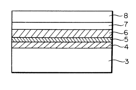
FIG. 2 is a schematical cross-sectional view of the
essential part of the optical information recording
medium according to this invention. This part comprises
a substrate 3, heat-resistant protective layers 4 and
6, an optical active layer 5 and a protective substrate 8
which is adhered to the heat-resistant protective layer
by an adhesive layer 7. This invention is featured by
materials specified for the heat-resistant protective
layers 4 and 6. That is, conventional materials such
as germanium dioxide (GeO2), silicon dioxide (SiO2)
and zinc sulfide (ZnS) do not provide any sufficient
mechanical strength and thermal properties.
A heat-resistant protective layer having a
poor mechanical strength at a high temperature, may be
broken due to thermal deformation when laser irradiated,
and further a heat-resistant protective layer having
many structural defects, may be shrinked by heat to
permanent deformation. With the thermal properties,
the protective layer should have a proper thermal
conductivity and specific heat, in order to effectively
utilize the thermal energy of laser. If the thermal
conductivity is too high, an extra amount of energy is
inconveniently required. If the thermal conductivity is
too low, the desired quenching conditions are not satis-
fied. The quenching conditions are important to the
phase change type optical information recording media,
because such media records and erases information by
129~912
1 reversible transformation from one phase to another
and vice versa with the combination of heating and
quenching or annealing.
The feature of this invention is to improve
the recording-erasing cyclability of an optical infor-
mation recording medium by controlling the thermal
constant of the medium while maintaining the high-
temperature mechanical properties at a good level or
restraining the outstanding thermal deformation to the
minimum and further to improve recording-erasing
cyclability. As actual conditions for designing the
protective layer it is desired that the protective
layer has a high efficiency of optical absorption for
laser. For this, incident laser light is necessary to
satisfy an antireflection condition. An active layer
containing tellurium as a principal constituent has a
refractive index of about 4. In order to obtain the
antireflection condition, the refractive index of the
heat-resistant protective layer should be less than
about 4, and calculation reveals that the refractive
index between 2 and 3 achieves optimum antireflection
condition. The antireflection condition is approximately
expressed by the following equation:
d = L / 4N
wherein N is the refractive index of the protective
layer, L the wavelength of a laser and d the thickness
-- 6 --
12~8912
1 of the protective layer. A typical material satisfying
the equation above is zinc sulfide (ZnS : N = 2.3).
As mentioned above, however, ZnS is excellent
in the intial characteristics but it was found according
to the inventors' experiments that the recording-erasing
cyclability was not satisfied. Therefore, the inventors
tried to improve this cyclability. As a result, they
have found that a mixture of zinc sulfide and silicon
dioxide has an excellent cyclability. Further inventors'
experiments have revealed that materials exhibiting novel
characteristics can fundamentally be obtained by
quenching or vapor depositing two mutually solid-insoluble
components to produce a thin film constituted by uniformly
finely divided and intimately mixed particles, which
look as if they are forcibly formed to be a solid solu-
tion. These components of the materials are featured
by being mutually solid insoluble, as mentioned above.
The combination of these mutually solid-insoluble
components is one of a glassy component and a crystalline
component. The crystalline component is a chalcogenide
such as a zinc chalcogenide such as ZnS, ZnSe or ZnTe,
or a lead chalcogenide such as PbS. The glassy material
is an oxide glass such as silicon dioxide or germanium
dioxide, or a non-oxide glass such as silicon nitride
or silicon carbide.
It has not yet been clear why the combination
of the crystalline constituent and the glassy constituent
brings about the desired effect of this invention.
-- 7 --
1291~912
1 Perhaps it appears that the presence of the glassy
constituent inhibits the growth of the crystalline
constituent as microstructural unit (grain or crystal
grain) in the thin film, so that the crystalline
constituent is refined or made amorphous, and that
the thin film of such refined crystalline or amorphous
component has a low thermal conductivity and hence
applied laser energy contributes to the efficient
increase in the temperature of the active layer.
The average size of the above-mentioned
microstructural unit is preferred to be smaller, and it
is most preferably as small as not observed by an X-ray
diffraction method. In this invention, the microstructural
unit means a size which can be observed as a crystallite
under a transmission electron microscope (TEM), i.e.,
a size (diameter) of grains observed from the diffraction
image of crystals. The grain size described below all
were determined in the above-mentioned manner. The
actual effect of this invention can be obtained at a
grain size of 10 nm or less, preferably 5 nm or less.
If the laser power is effectively absorbed
into the active layer, a less amount of the laser power
irradiated is satisfactory. This means that the ambient
temperature of the active layer is not raised when
recorded and erased. Conclusively, the thermal damage
of the active layer and the heat-resistant protective
layer is reduced and the recording-erasing cyclability
are increased, which means that the cyclability of the
~2~gl2
1 optical information recording medium are improved by
this invention. Therefore, the lower laser power
required for recording and erasing is essential to the
increase in the cyclability.
It has already been confirmed that the number
of recording-erasing cycles on a static tester is at
least 106 for a medium having a heat-resistant protective
layer, which is improved in the recording and erasing
sensitivity unless otherwise indicated in the examples
below.
Generally, a chalcogenide has a great refractive
index, i.e., it can satisfy the requirement of N > 2.
Many oxide glasses have a refractive index of at most
2. Therefore, it is generally understandable that the
forced admixing of an excessive amount of the glassy
constituent to the chalcogenide has an adverse effect on
the characteristics of the medium, but it has been found
that a moderate amount can give conspicuously improved
characteristics.
This invention will be illustrated below with
reference to some examples.
EXAMPLE 1
A heat-resistant protective layer comprising
a mixture of zinc sulfide (ZnS) and silicon dioxide (SiO2)
was formed by the binary-source deposition system on
a substrate of polymethyl methacrylate (PMMA). The
schematical view of an evaporation apparatus used in this
~9~9 12
1 example is shown in FIG. 3. The reached vacuum degree
was in order of 10 6. A vacuum chamber 7 was evacuatéd
at an evacuation vent 12. A substrate 8 was rotated by
a rotating axis 9. Evaporation of the components, zinc
sulfide and silicon dioxide were carried out at
evaporation sources 10 and 11. The mixing ratio of
zinc sulfide and silicon dioxide was determined by
controlling the evaporated amounts of the respective
components, and qualitative chemical analysis was carried
out. As the material of the active layer was used a
TeGeSnO system compound, which is one of the phase
change type materials which is recordable and erasable by
changing from the crystalline phase to the amorphouse
phase and vice versa. The thickness of the active layer
was 100 nm. The heat-resistant protective layers were
formed both between the active layer and the substrate
and on the active layer. The protective layers had a
thickness of 100 and 200 nm, respectively. These thick-
nesses were decided in view of a laser abæorption effici-
ency and a great change in the optical constant.~
FIG. 4 shows a relationship between the mixingratio (x) of SiO2 and the refractive index of the heat-
resistant protective layer itself. This shows that the
refractive index is nearly linearly reduced as the
addition of SiO2 to ZnS is increased. This means that
ZnS and SiO2 are not bonded to each other but simply
mixed. The same relationship can be seen in combinations
other than that of ZnS and SiO2, which are described in
-- 10 --
lZ~8~12
1 the examples below.
Table 1 represents the relationship between
the addition of SiO2 and the minimum power required
for crystallization (erasing) and amorphization
(recording). Table 1 also shows the average grain size
of ZnS determined by the transmission electron micro-
scope.
This determination was dynamically carried out
by rotating a disk at a peripheral speed of about 5 m/sec.
A laser used had a wavelength of 830 nm and its beam was
focused on the disk to the diffraction limit. The
laser power was as small as possible, in order to diminish
the load on the disk.
Table 1: Effect of Addition of SiO2 to ZnS
Amount of SiO2 Minimum Laser Power Grain Size
(mol%) (mW) (nm)
Recording Erasing
0 9 14 30
9 14 30
7.5 12.5 10
6 12 5
6 12 5
8.5 13 <5
From Table 1 it is seen that when the amount
of SiO2 added is 10 to 30 mol%, the grain size is 10 nm,
12~gl2
1 which reveals that there was effectiveness. The addition
of SiO2 to ZnS allows the minimum power required for
crystallization and amorphization to be reduced, and
further addition allows the power to be again raised.
This shows that there is an optimum amount of SiO2 added.
In this example, it is seen that when the amount of SiO2
added is between 10 and 30 mol%, the laser power required
for crystallization is 6 to 7.5 mW, which is lower than
the power (9 mW) required in the case free of SiO2. At
this amount added, the refractive index is about 2 or
more, which satisfi~s the above-mentioned optical require-
ment.
As is clear from the above, the addition of
SiO2 to ZnO is effective to reduce the laser power re-
quired for crystallization.
FIG. 5 shows a change in the reflectivity onrecording and erasing cycles by using a static tester.
In FIG. 5, there are five pairs of curves, each of which
pairs has the upper curve corresponds to crystallized
state, i.e., erased state and the lower curve corresponds
to an amorphized state, i.e., recorded state. A dif-
ference in the reflectivity is in proportion to the
intensity of signals to be recorded. From FIG. 5, it
is seen that the addition of SiO2 causes the number of
recording-erasing cycles to be changed. The laser power
was determined so as ~o simulate the thermal load in
the disk.
The projection of a laser power distribution
- 12 -
lZ98~12
1 on the disk was,adjusted so that it was in a circular
shape for recording and in an ellipsoidal shape for
erasing.
In this case, it is also seen that the best
result was obtained when the amount of SiO2 added was
20 mol%, and that it is possible to repeat recording-
erasing cycles 106 times.
In this example, SiO2 and ZnO were forcibly
dispersed and mixed by quenching from their vapor
phases to achieve the desired characteristics. However,
annealing from the same vapor phases, for example, at an
extremely low deposition rate, prevents the dispersion
and accelerates phase separation, thereby not improving
the sensitivity as well as not increasing the number
of recordins-erasing cycles. This is the same as in
the examples described below.
EXAMPLE 2
A heat-resistant protective layer comprising
a mixture of zinc selenide (ZnSe) and silicon dioxide
(SiO2) was formed by the binary-source deposition system
on a substrate of polymethyl methacryla~e. The reached
vacuum degree was in order of 10 6. The mixing ratio
of zinc selenide and silicon dioxide was decided by
controlling the evaporated amounts of the respective
materials in the same manner as in EXAMPLE 1. The
quantitative chemical analysis was carried out. As the
material of the active layer was used the same TeGeSnO
1;2~8~12
1 system compound as in EXAMPLE 1. The thickness of the
active layer was 100 nm. The heat-resistant protective
layers were provided on the active layer at both the
substrate side and the opposite side thereof with thick-
nesses of 100 and 200 nm, respectively.
FIG. 6 represents a relationship between the
refractive index and the amount (x) of SiO2 added of
the heat-resistant protective layer itself. It is
clear from FIG. 6 that the refractive index is nearly
linearly decreased as the amount of SiO2 to ZnSe is
increased.
Table 2 shows the relationship between the
amount of SiO2 added and the minimum laser power required
for the crystallization and amorphization. The measure-
ment method was the same as in EXAMPLE 1.
Table 2: Effect of Additon of SiO2 to ZnSe
Amount of SiO2 Minimum Laser Power
(mol%) ~mW)
Recording Erasing
0 9 14
9 14
7.5 13
6 12
6 11.5
8.5 13.5
- 14 -
129~912
1 The addition of SiO2 to ZnSe allows the laser
power required for the crystallization and amorphization
to be reduced and further addition allows the laser
power to be increased, as in EXAMPLE 1. As is seen from
the results that there is an optimum amount of SiO2
added.
In this example, it is understood that if the
amount of SiO2 added is 15 to 35 mol~, the laser power
required for the crystallization is in the range of 6
to 7.5 mW, which is lower than that of the layer free
of SiO2 (9 mW).
As is clear from the above, the addition of
SiO2 to znse can achieve the effect of reducing the laser
power required for the crystallization and amorphization.
This heat-xesistant protective layer withstood 106
recording-erasing cycles on a static tester, as in
EXAMPLE 1.
EXAMPLE 3
A heat-resistant protective layer comprising
a mixture of a zinc chalcogenide, i.e., zinc sulfide
(ZnS), zinc selenide (ZnSe) or zinc telluride (ZnTe) with
any glassy oxide of germanium dioxide (GeO2), tin oxide
(SnO2), indium oxide (In2O3) and tellurium dioxide
(TeO2) was formed by the binary-source deposition system
on a substrate of polymethyl methacrylate. The mixing
ratio of the zinc chalcogenide (ZnX : X is a chalcogen~
and the glassy oxide was decided by controlling the
- 15 -
~2'3~12
1 respective amounts of the materials evaporated. The
quantitative chemical analysis was also carried out. As
the material for the active layer was used the same
TeGeSnO system compound as in EXAMPLE 1. The thickness
of the active layer was 100 nm. The heat-resistant
protective layers were provided on the active layer at
both the substrate side and the opposite side thereof,
in thicknesses of 100 nm and 200 nm, respectively.
Table 3 shows the relationship between the
amount of the oxide added and the minimum laser power
required for the crystallization and amorphization.
The measurement method was the same as in EXAMPLE 1.
The addition of the glassy oxide to zinc
chalcogenide allows the minimum laser power required
for the crystallization to be reduced, and further
addition allows the minimum power to be increased
again. From this it is clear that there is an optimum
amount of the glassy oxide added.
In this example, it is seen that when the
amount of SnO2 added was in the range of 15 to 35 mol~,
the laser power required for the crystallization was
in the range of 6 to 7 mW, which was lower than that of
the protective layer free of the SnO2 (9 mW). Further-
more, it is seen that the laser power required for the
amorphization was reduced.
Substantially the same results were obtained
for the combinations of the two other chalcogenides
and the oxide.
12~8912
Table 3: Effect of Addition of GeO2 to ZnS
Amount of GeO2 Minimum Laser Power
(mol%) (mW)
Recording Erasing
0 9 14
9 14
7 13
6 12
6 12
7.5 13
1 EXAMPLE 4
A heat-resistant protective layer comprising
a mixture of zinc sulfide and glassy silicon nitride
(Si3N4) was formed by the binary-source deposition system
on a substrate of polymethyl methacrylate. The mixing
ratio of zinc sulfide and glassy silicon nitride was
decided by controlling the evaporated amounts of the
respective materials in the same manner as in EXAMPLE 1.
The quantitative chemical analysis was carried out.
The active layer was made of the same material as used
in EXAMPLE 1, TeGeSnO. The thickness of the active
layer was 100 nm. The heat-resistant protective layers
were provided on the active layer at both the substrate
side and the opposite side thereof, in thicknesses of
100 and 200 nm, respectively.
Table 4 shows a relationship between the amount
- 17 -
lZ~3912
1 of Si3N4 added and the minimum laser power required for
the crystallization and amorphization.
Table 4: Effect of Addition of Si3N4 to ZnS
Amount of Si3N4 Minimum Laser Power
(mol%) (mW~
Recording Erasing
0 9 14
9 14
7.5 12.5
6 12
6.5 12.5
8.5 14
FIG. 7 shows a relationship between the amount
of Si3N4 added and the refractive index of the heat-
resistant protective layer itself obtained in thisexample. From FIG. 7 it is clear that the refractive
index is nearly linearly reduced as the amount of
Si3N4 added to ZnS is increased. In this example, it
was confirmed that the minimum laser powder required for
the crystallization and amorphization was reduced by
adding Si3N4 to ZnS in the heat-resistant protective
layer. This reveals that there is an optimum value in
the amounts of Si3N4 added to ZnS. That is, the optimum
value is about 20 mol%.
- 18 -
12~& 1;~
1 EXAMPLE 5
A heat-resistant protective layer comprising
a mixture of zinc selenide and glassy silicon carbide
(SiC) was formed by the sputtering method on a
substrate of polymethyl methacrylate. FIG. 8 shows a
schematical view of a sputtering apparatus used in
this example, and FIG. 9 shows the structure of a cathode
target used in the sputtering apparatus. In FIGS. 8 and
9, reference numbers 13, 14, 15, 16, 17 and 18 are a
vacuum chamber, substrate, cathode material, adjusting
cathode material, evacuation vent and rotating axis,
respectively. The adjusting cathod materials were
arranged in a mosaic form for adjusting the composition
to be sputtered. This sputtering apparatus was
commercially available. The cathode target was of a
composite type. That is, a sintered body of ZnSe and
sintered pellets of SiC on the sintered body in a desired
mixing ratio thereof were sputtered. The quantitative
chemical analysis was carried out. The active layer
was made of the same TeGeSnO as used in EXAMPLE 1.
The thickness of the active layer was 100 nm. ~he
heat-resistant protective layers were provided on the
active layer at the substrate side and the opposite
side thereof, in thicknesses of about 100 and 200 nm,
respectively.
This example also confirmed that the addition
of SiC to ZnSe reduced effectively the minimum laser
power required for the crystallization and amporphization.
-- 19 --
~29~912
1 The optimum amount of SiC to ZnSe was about 20 mol%.
EXAMPLE 6
A heat-resistant protective layer comprising
a mixture of zinc sulfide, silicon dioxide and germanium
dioxide was provided by a ternary-source deposition
sys~em on a substrate of polymethyl methacrylate. The
content of zinc sulfide was constant (15, 20 and 50
mol%) and the amounts of silicon dioxide and germanium
dioxide added were changed. The respective effects
were measured. The mixing ratios thereof were decided
by controlling the evaporated amounts of the respective
materials. The quantitative chemical analysis was
carried out. The active layer was made of the same
TeGeSnO as used in EXAMPLE 1. The thickness of the
active layer was 100 nm. The heat-resistant protective
layers were formed on the active layer at both the
substrate side and the opposite side thereof in thick-
nesses of 100 and 200 nm, respectively.
FIG. 10 shows a relationship between the
amounts of SiO2 and GeO2 added and the refractive index
of the protective layer. From FIG. 10 it is seen that
as the amount of a mixture of SiO2 and GeO2 to ZnS is
increased, the refractive index is nearly linearly
decreased. FIG. 11 shows a relationship between the
total amount of the glassy oxides added and the minimum
laser power required for the crystallization. The
minimum laser power was reduced to the lowest level,
- 20 -
1 i.e., 6 mW when the total amount was about 20 mol~.
The laser power for the amorphization was 2 mW reduced.
The measurement method was the same as used in EXAMPLE
1.
EXAMPLE 7
A heat-resistant protective layer comprising
a mixture of a lead chalcogenide (PbS, PbSe and PbTe)
and silicon dioxide was provided by the binary-source
deposition system on a substrate of polymethyl meth-
acrylate. The reached vacuum degree was in order of10 6. The mixing ratios of the lead chalcogenide and
silicon nitride were decided by controlling the
evaporated amounts thereof, as in EXAMPLE 1. The
quantitative chemical analysis was carried out. The
active layer was made of the same TeGeSnO as used in
EXAMPLE 1 and the thickness of the active layer was 100
nm, The heat-resistant protective layers were provided
on the active layer at the substrate side and the
opposite side thereof in thicknesses of about 100 and
200 nm, respectively.
FIG. 12 shows a relationship between the
amount of SiO2 added to PbTe and the refractive index
of the heat-resistant protective layer. From FIG. 12
it is seen that as the amount of SiO2 added is increased,
the refractive index is nearly monotonously reduced.
The minimum laser power required for the crystallization
and amorphization was measured in the same manner as
- 21 -
12~912
1 in EXAMPLE 1. It was reduced with the lead chalcogenide
but the extent of the reduction in the minimum laser
power was smaller than that with the zinc chalcogenide.
This example also confirmed that there was the optimum
amount of SiO2 added, but this effect with the lead
chalcogenide was smaller than that with the zinc
chalcogenide. The reason therefor is considered that
the lead chalcogenide has a slight amount of absorption
at a wavelength of semiconductor laser.
EXAMPLE 8
A heat-resistant protective layer comprising
a mixture of zinc selenide (ZnSe) and silicon dioxide
(SiO2) was provided by the binary-source deposition
system on a substrate of a ~olycarbonate. The
reached vacuum degree was in order of 10 6. The
mixing ratio of zinc sulfide and silicon dioxide was
decided by controlling the evaporated amounts of the
respective materials, as in EXAMPLE 1. The quantitative
chemical analysis was carried out. The active layer was
made of TbFeCo for magneto-optical media. The thickness
of the active layer was S0 nm. The heat-resistant
protective layers were formed on the magneto-optically
active layer at both the substrate side and the opposite
side thereof in thicknesses of about 100 and 200 nm,
respectively. The resultant heat-resistant protective
layers were similar to those of EXAMPLE 2. Table 5
shows the relationship between the amount of SiO2 added
- 22 -
1298912
1 and the oxidation resistance of the protective layers.
In the case of ZnS alone, the reflectivity thereof was
reduced after a few days, but the ZnS having SiO2 added
hereto was not reduced even after 30 days.
Table 5: Addition of SiO2 and Oxidation
Amount of SiO2 Change in Reflectivity
(mol~) (%)
After 3 days After 30 days
0 -20 ***
- 5 -35
0 - 5
0 - 6
As is seen in the examples described above,
this invention is effective in improving the character-
istics of the optical information recording medium.
Particularly, this invention is highly effective at the
points that the incident laser power is effectively
utilized, that the cyclability of recording-erasing is
increased, and that the active layer is protected from
oxidation. Thus, this invention is advantageous in
improving the cyclability of the optical information
recording medium.
The examples above reveal that a crystalline
material such as zinc sulfide and a glassy material such
as silicon dioxide were quenched from the vapors thereof
to form a thin layer comprising finely divided particles
- 23 -
~L2~8912
1 which look as if they are forcibly allowed to form a
solid solution. This concept is novel over prior art.
EXAMPLE 9
In EXAMPLE 1, sio2 and ZnS were forcibly dis-
persed and mixed by the quenching of vapors or vapor
despotion, in which the deposition rate was 1 nm/sec.
On the other hand, amIealing from the same vapor phases
at an extremely low deposition rate causes an average
grain size of ZnS to be too great for the ZnS grains to
be dispersed and the phase separation to be accelerated,
thereby not improving the senstivity of recording and
erasing as well as not increasing the number of recording-
erasing cycles. In order to confirm this cause, the
degree of dependency of the sensitivity of the laser
power to recording and erasing upon the vapor deposition
rate at an amount of SiO2 added being 25 mol% was measured.
The results are reported in Table 6.
Table 6: Vapor Deposition Rate, Grain Size and
Sensitivity of Laser Power to Recording
and Erasing
Deposition Rate Grain Size Minimum Laser Power
Recording Erasing
(nm/sec) (nm) (mW)
3 <5 5.5 12
2 5 6 12
1 5 6 12
0.5 10 6.5 13
0.2 15 8 14
0.1 30 9 14
- 24 -
1 From Table 6 it is seen that when the grain
size is great, the laser power is excessively required,
which means that the sensitivity is poor. Furthermore,
it is clear that the grain size should be 10 nm. These
are common to the following examples.
EXAMPLE 1 0
A heat-resistant protective layer comprising
a mixture of zinc selenide (ZnSe) and silicon dioxide
(SiO2) was provided by the binary-sourse deposition
system on a substrate of polymethyl methacrylate. The
reached vacuum desree was in order of 10 6. The mixing
ratio of zinc selenide and silicon dioxide was decided
by controlling the evaporated amounts of the respective
materials. The quantitative chemical analysis was
carried out. The active layer was made of the same
TeGeSnO as us~d in EXAMPLE 1. The thickness of the
active layer was 100 nm. The heat-resistant protective
layers were formed on the active layer at the substrate
side and the opposite side thereof in thicknesses of
100 and 200 nm, respectively. Table 7 shows a relation-
ship between the amount of SiO2 added and the minimum
laser power required for the crystallization and
amorphization. The measurement method was the same as
used in EXAMPLE 1.
- 25 -
~29~3~12
Table 7: Effect of Addition of SiO2 on ZnSe
Amount of SiO2 Minimum Laser Power Grain Size
(mol%) (mW) (nm)
Recording Erasing
0 9 14 30
9 14 20
7.5 13 10
6 12 5
6 11.5 5
8.5 13.5 <5
1 Table 7 also shows the average grain size
of ZnSe observed under a transmission electron microscope.
From Table 7 it is seen that the addition of SiO2 to
ZnSe allowed the laser power required for the crystal-
lization and amorphization to be reduced and further
addition allowed the laser power to be increased again.
Thus, it is understood that there is an optimum amount
of SiO2 added.
In this example, it is seen that when the amount
of SiO2 added was in the range of 15 to 35 mol%, the
grain size was less than 10 nm and the laser power
required for the crystallization and amorphization was
in the range of 6 to 7.5 mW, which was effectively lower
than that in the case free of SiO2 (9 mW).
Furthermore, it was found that the heat-
resistant protective layer with the above-mentioned mixing
ratio can withstand 106 or more recording-erasing cycles,
- 26 -
~Z~ 2
1 as in EXAMPLE 1.
EXAMPLE 11
A heat-resistant protective layer was provided
by the binary-source deposition system on a substrate of
polymethyl methacrylate. The heat-resistant protective
layer was comprised of a mixture of a zinc chalcogenide
such as zinc sulfide (ZnS), zinc selenide (ZnSe) or zinc
telluride (ZnTe) with any oxide of glassy germanium
dioxide (GeO2), tin oxide (SnO2), indium oxide (In2O3)
and tellurium oxide tTeO2). The mixing ratio of the
zinc chalcogenide (ZnX: X is a chalcogen) and the glassy
oxide was decided by controlling the evaporated amounts
of the respective materials, as in EXAMPLE 1. The
quantitative chemical analysis was carried out. The
active layer was made of the same TeGeSnO as used in
EXAMPLE 1. The thickness of the active layer was 100 nm.
The heat-resistant protective layers were formed on the
active layer at the substrate side and the opposite side
thereof in thicknesses of 100 and 200 nm, respectively.
Table 8 shows a relationship between the
amount of the oxide added and the minimum laser power
required for the crystallization and amorphization.
The measurement method was the same as used in EXAMPLE 1.
The addition of the glassy oxide to the zinc chalco-
genide allowed the minimum laser power required for the
crystallization and amorphization to be reduced and
further addition allowed it to be increased again. From
- 27 -
129~9~2
1 this it is understood that there is an optimum amount
of the glassy oxide added.
In this example, when the amount of SnO2
added was in the range of 15 to 35 mol~, the grain size
was 10 nm or less, and the laser power required for the
crystallization was in the range of 6 to 7 mW, which was
lower than that in the case free of the glassy oxide.
Furthermore, the laser power required for the amorphiza-
tion was also reduced. Substantially the same results
were obtained for the combinations of the two other zinc
chalcogenides and oxides.
Table 8: Effect of Addition of GeO2 to ZnS
Amount of GeO2 Minimum Laser Power Grain Size
(mol%) (mW~ (nm)
Recording Erasing
0 9 14 35
9 14 30
7 13 20
2~ 6 12 10
6 12 5
7.5 13 <5
Table 8 also shows the average grain size of
ZnS observed under a transmission electron microscope.
From the examples above, it is concluded that
the optical information recording medium according to
- 28 -
1 this invention has an improved characteristics,
particularly it is excellent at the points that incident
laser power is effectively utilized, that the number
of recording-erasing cycles is increased, and that the
heat-resistant protective layer of this invention can
well protects the active layer from oxidation and hence
it is highly reliable.
The explanation of this invention a~ove
refers particularly to an appliclation to an optical
disk, since this invention is also featured by the
structure of the disk. However, the heat-resistant
pro~ective layer according to this invention may also
be utilized as a passivation membrane using the thermal
characteristics thereof, or as a thin film head or
thermal printer using an insulation characteristics
thereof.
- 29 -