Note: Descriptions are shown in the official language in which they were submitted.
J 2C~
~ 1 --
PROTECTION OF THYRISTORS DURING TURN-ON
This invention relates to thyristors, and, mo,re
particularly to the protection of thyristors during
adverse turn-on conditions prior to the "recovery time".
A thyristor is turned on by application of a current
pulse to a gate electrode. This results in the emitter-
base junction at the cathode becoming forward biased and
conduction occurring through the device in a bulk
conducting volume between the main cathode and the anode,
this being known as forward conduction. Thyristor turn-
off and subsequent "recovery" is achieved by applying areverse bias across the anode and cathode electrodes of
the device to reduce current flow below the thyristor
holding level. The current flow through the thyristor
first decreases to zero (known as current zero) and then
becomes negative as charge carriers in the device are
extracted, and as the depletion layer of the reverse
blocking junction forms. At current zero the device still
contains charge carriers in its base regions, which cannot
be removed easily once the depletion layer of the blocking
junction forms. Such charge carriers recombine at a rate
determined by the carrier lifetimes of the base regions.
If a positive voltage ramp is now applied across the
thyristor at some time after current zero, a displacement
current is generated, which has a magnitude determined by
the rate of rise of the voltage ramp and the forward
0
junction capacitance. If the voltage across the device
reaches zero volts, any unrecombined charge begins to flow
from the base regions: the sum of the extracted
unrecombined charge current and the displacement current
is collectively known as the forward recovery current and
can trigger the thyristor back into a forward conduction
state. Importantly, the magnitude of this current depends
on the amount of unrecombined charge still remaining in
the base regions of the thyristor at the time of
application of the positive voltage ramp and the rate of
rise of the voltage ramp. If the forward recovery current
is small the thyristor is not turned on, and the voltage
across the thyristor continues to rise. However, the
forward recovery current may be large enough to cause the
base-emitter junction to become sufficiently forward
biased as to turn-on the thyristor. If a large amount of
unrecombined charge still exists in the base regions when
the voltage ramp is applied, turn-on occurs fairly
uniformly across the thyristor. In this case, the
relatively low energy dissipation density results in the
thyristor being turned on non-destructively. However, a
problem may arise when a positive voltage is applied at a
time after curent zero when only a few unrecombined
carriers still remain in the base regions of the device.
In this situation, turn-on may occur in only a small
volume of the thyristor, whereby the energy dissipated
could cause the small initial turned-on region to become
~ ,~
2C~
so hot that the device is destroyed. This may happen even
where the rate of rise of the voltage ramp is relatively
small. For a given positive voltage ramp condition, the
minimum time beteen current zero and the point where zero
voltage appears across the thyristor such that turn on
does not occur, is known as the "thyristor recovery time"
Previous methods for preventing damage to the
thyristor during such adverse turn-on conditions, when a
voltage is reapplied shortly after applying a reverse bias
but prior to the end of the thyristor recovery time, have
employed expensive external circuitry to monitor the
positive ramp voltage to be applied and bias on the device
conventionally before damage can occur. However, such
circuitry is complex and potentially unreliable.
The present invention seeks to provide a thyristor
having improved protection against this adverse turn-on
condition.
According to this invention, there is provided a
thyristor comprising a region of relatively long carrier
lifetime compared to that of a bulk conducting volume, the
region being located at such distance from the bulk
conduc'ting volume that, during conduction, sufficent
charge carriers enter the region from the bulk conducting
volume, whereby under adverse turn-on conditions prior to
the end of the thyristor recovery time, initial turn-on
occurs at the region. The location of the region and its
geometrical dimensions must be carefully chosen for
lf~ 9ZO
optimum performance. By including a region of relatively
long carrier lifetime in accordance with the invention, it
is possible to ensure that turn on is initiated in-that
region and thus that the thyristor is protected against
S destructive turn-on after conduction through the bulk
conducting volume has reached current zero. It has been
found that, advantageously, the relatively long carrier
lifetime is approximately two or more times the carrier
lifetime in the bulk conducting volume.
In previous devices, such adverse turn-on conditions
in which a positive voltage ramp is applied a short time
after current zero would have resulted in partial turn-on
in the bulk conducting volume with possible damage. The
application of such a voltage ramp at that time across a
thyristor in accordance with the invention however,
results in turn-on being initiated in the regi~n of
relatively long carrier lifetime, where enough
unrecombined carriers exist to provide turn-on. In a
preferred embodiment of the invention, an amplifying gate
arrangement with integral current limiting resistors is
used to prevent damage to the region and to allow the
remainder of the thyristor to turn on.
The region may be located close to the bulk
conducting volume, say within approximately four carrier
diffusion lengths of it. However, this may not be an
appropriate location because of design and/or
manufacturing constraints. Advantageously therefore there
l'~9~g20
-
may be included an intermediate zone of long carrier
lifetime located between the region and the bulk
conducting volume. Such an arrangement enables the long
lifetime region in which initial turn-on occurs during
adverse turn-on conditions to be positioned further from
the bulk conducting volume than would otherwise be
practicable, since charge carriers entering the
intermediate zone from the bulk conducting volume will
exist for a sufficient time for them to cross the zone to
10 the region where turn-on occurs. It has been found that
preferably, the region is located within approximately
four carrier diffusion lengths of the bulk conducting
volume.
It is preferred that the region is such that a
15 smaller charge carrier density than that of the bulk
conducting volume is required for turn-on to occur. This
may be achieved by arranging that the conduction path
through the region is shorter than that through the bulk
conducting volume. For example, an emitter region and
20 metallisation layer at the region may be recessed into it
to form a "well" configuration. The region is thus of
high c~rrent gain.
Preferably, a current limiting resistor is included
and arranged adjacent the region. The current flow
25 through the initial turned-on area may then be restricted
and damagingly high current densities prevented.
Preferably, the region is surrounded by current limiting
,.
~Z~20
resistors.
Preferably, a plurality of regions of relatively long
carrier lifetime are included. These may be distributed
in such a way to give more uniform turn-on across the
whole device. Also, by including a plurality of such
regions, it is probable that at least one region is
located adjacent to the last part of the main cathode to
cease conduction, and thus that the charge carriers exist
in that region for a maximum time after conduction has
10 ceased.
According to an aspect of the invention, a method of
manufacturing a thyristor in accordance with the invention
includes masking part of a semiconductor body where it is
desired to have a region of relatively long carrier
15 lifetime and producing a greater density of damage sites
in the unmasked portion than in the masked part. The
damage sites could be produced by well established
processing techniques such as electron irradiation. The
carrier lifetime could alternatively be modified by using
20 masked gold or platinum diffusion for example.
The invention is now further described by way of
example with reference to the accompanying drawing, in
which the sole figure schematically illustrates a
thyristor in accordance with the invention.
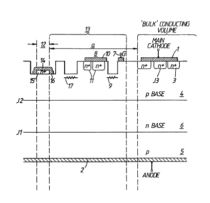
With reference to the Figure, a thyristor includes a
main cathode electrode 1 and an anode electrode 2 between
which current flows during conduction through the device.
, .~
- ~298920
",
-- 7
An n-emitter region 3 is located adjacent the cathode
electrode 1 and forms a junction J3 with a p-base region
4. A p-diffused anode region 5 is located adjacent the
anode electrode 2 and an n-base region 6 lies between the
two p-base regions 4 and 5.
To initiate conduction, a current is applied to a
gate electrode 7 and flows through the p-base region 4 to
the cathode 1. This current flow causes the junction J3
to become forward biased and electrons are injected into
the p-base region 4 from the n-emitter region 3. The
electrons are accelerated across a depletion layer
associated with the junction J2 between the p-base region
and the n-base region 6. Electrons diffuse through the n-
base region 6 and cause hole injection from the p-base
anode 5, and conduction occurs through the thyristor. It
is desirable that the bulk conducting volume between the
cathode 1 and the anode 2 has a relatively short carrier
; lifetime in the vicinity of the junction J2 between the p-
base region 4 and the n-base region 6. Then, when reverse
bias is applied across the thyristor to turn it off, there
is relatively rapid recombination with a correspondinqly
short recovery time.
Following commutation of the thyristor, (i.e. when
the bias is reversed), reverse recovery current flows
until carriers have been excluded from the reverse
blocking junction Jl and the depletion layer forms.
Excess carriers remain in the base regions 4 and 6 and
~ .
,-:
12~2~
recombine at a rate determined by their lifetimes in these
regions
The thyristor includes an auxiliary thyristor 8
separated from the main cathode 1 by a current limiting
resistor 9. The auxiliary thyristor 8 includes a
metallisation layer 10 and an n-emitter region 11
The thyristor also includes a long lifetime region
indicated at 12 and generally located within about four
carrier diffusion lengths from the bulk conducting volume
10 between the main cathode 1 and anode 2 at a distance a.
In the thyristor shown in the Figure, the n-base region 6
in the long lifetime region 12 is arranged to have a
relatively long carrier lifetime, being approximately two
times the carrier lifetime in the bulk conducting volume.
15 An intermediate zone 13 which also has a long carrier
lifetime is located between the region 12 and the bulk
conducting volume, and in this embodiment has
approximately the same carrier lifetime as region 12. The
intermediate zone 13 is contiguous with the region 12 and
20 less than one carrier diffusion length from the bulk
conducting volume. A metallised surface layer 14 and an
n-emitter region 15 are included at the long lifetime
region 12 forming a higher gain thyristor structure which
is connected, via a p-base short 16 and a current limiting
25 resistor 17, to the auxiliary thyristor 8 which is located
at the intermediate zone 13.
After current zero but prior to the end of the
Z9~210
g
recOvery time, charge carriers recombine more slowly in
the long lifetime region 12 and intermediate zone 13 than
in the bulk conducting volume. Thus near to the end of
the thyristor recovery time many unrecombined carriers
still exist in region 12 and zone 13 whereas few remain
within the bulk conducting volume. If a positive going
voltage ramp is applied across the thyristor, so that it
becomes forward biased, prior to the elapse of the
thyristor recovery time, many holes flow through the p-
base 4 beneath the n-emitter region 15 of the high current
gain long lifetime region 12. This causes the p-base - n-
emitter junction at the long lifetime region 12 to become
forward biased, initiating turn-on at that part of the
device. The limiting resistances 9 and 17 ensure that
current flow through the initially small turned-on area in
the long lifetime region 12 is kept below damagingly high
levels. The current flowing through the long lifetime
region 12 then turns on the rest of the device via the
auxiliary thyristor 8. Although only one long lifetime
region has been shown, it may be advantageous to have a
plurality of such regions distributed throughout the
device.
The long carrier lifetime regions 12 and 13 are
produced using well known processing techniques during
manufacture of the thyristor. The semiconductor body on
which the thyristor is formed initially has long carrier
lifetimes throughout. During manufacture, a metal masking
.A~ . .
-- 10 --
layer for example, is laid down on the thyristor surface
over those areas which it is desired to leave with a long
carrier lifetime. The body is then irradiated, for
example, with a high energy (2-10 MeV) electron beam. The
S irradiation causes damage sites to be produced in unmasked
parts of the substrate. The damage sites act as
recombination centres and hence carrier lifetimes are
reduced in the unmasked portion.
.