Note: Descriptions are shown in the official language in which they were submitted.
~z99z~
OPTICAL RECEIVERS
This invention relates to optical receivers, and is
particularly concerned with an optical receiver including a photodiode
and a transimpedance amplifier.
It is known from an article entitled "Atlanta Fiber System
Experiment: Optical Detector Package" by R.G. Smith et al. in the
Bell System Technical Journal, Vol. 57, No. 6, July-August 1978, pages
1809 to 1822 to provide an optical receiver comprising an avalanche
photodiode (APD) coupled to a transimpedance amplifier. The
transimpedance amplifier is a shunt feedback amplifier which acts as a
current-to-voltage transducer providing an output voltage determined
by the photodiode current multiplied by the feedback resistance. It
has the advantages of being less noisy for a given bandwidth than an
unequalized amplifier which does not employ feedback, and having a
larger dynamic range than, and not requiring individual adjustment as
does, an equalized amplifier.
It is also known from an article entitled "Detectors -
Inexpensive p-i-n photodiodes match fiber, source characteristics" by
P.H. Wentland et al. in Electronics, August 5, 1976, pages 101 and 102
to provide an optical receiver comprising a high performance p-i-n
type silicon photodiode coupled to a transimpedance amplifier.
A problem with such known optical receivers is that the
photodiode is reverse biassed via a load resistor which must have a
relatively high resistance in order to minimize noise. This
resistance, in conjunction with the reverse bias supply voltage,
limits the upper level of photocurrent which can be accommodated, and
hence limits the dynamic range of the optical receiver. There is thus
a direct conflict between the desire for a high resistance to minimize
noise and a low resistance to maximize dynamic range. Typically, a
relatively high resistance has been used in conjunction with a
relatively high voltage power supply to increase the upper limit of
photodiode current. It would be desirable to eliminate the need for
such a high voltage power supply, and to reverse bias the photodiode
from the same power supply, typically having a low voltage of 5 volts,
as is used for other parts of an optical receiver arrangement. In
addition, it is desirable to use most of the supply voltage for
12~9;2~5
reverse biassing the photodiode and thereby reducing its capacitance
and improving its speed and noise characteristics.
An object of this invention, therefore, is to provide an
improved optical receiver.
According to one aspect of this invention there is provided an
optical receiver comprising a photodiode which is reverse biassed via
a forward biassed semiconductor diode.
In such an optical receiver, the forward biassed semiconductor
diode provides a desirable load impedance for the reverse biassed
photodiode, without necessitating a large voltage drop at high
photocurrent levels and without significantly affecting noise and
dynamic range characteristics. The relatively low forward voltage
drop across this semiconductor diode enables low supply voltage
levels, of the order of 5 volts, to be used for biassing the
combination of the photodiode and load impedance.
The optical receiver preferably includes a transimpedance
amplifier having an input and an output, and coupling means coupling
the input of the transimpedance amplifier to a junction between the
photodiode and the semiconductor diode. The coupling means can
comprise a capacitor, but desirably this junction is connected
directly to the input of the transimpedance amplifier, which may
include a.c. coupling internally between ;nput and output stages
thereof.
In an embodiment of the invention, the optical receiver
includes signal compressing means, conveniently comprising two diodes
connected in parallel with one another with opposite polarities, a.c.
coupled between the output of the transimpedance amplifier and a
terminal of the semiconductor diode remote from said junction.
In another embodiment of the invention, the transimpedance
amplifier comprises an amplifier having an inverting input and an
output coupled respectively to the input and the output of the
transimpedance amplifier, and a capacitance coupled between the input
and the output of the transimpedance amplifier.
In a development of this embodiment of the invention the
photodiode is coupled between the input and the output of the
amplifier, the capacitance comprising a capacitance of the photodiode.
In this case the optical receiver may include a potential divider,
~2992~5
constituting an attenuator, coupled to the output of the amplifier the
photodiode being coupled to a tapping point of the potential divider
and thereby to the output of the amplifier. The potential divider is
conveniently a capacitive potential divider to avoid introducing
noise, as would be the case using a resistive potential divider.
The invention also provides an optical receiver arrangement
comprising such an optical receiver and a filter circuit coupled
thereto, the filter circuit comprising a bipolar transistor having a
base coupled to the output of the transimpedance amplifier, a
collector for producing a filtered output signal, and an emitter; an
open circuit transmission line having a characteristic impedance and a
predetermined length; and an emitter impedance matched to the
characteristic impedance coupling the transmission line to the
emitter.
Accordlng to another aspect of this invention there is
provided an optical receiver comprising: an amplifier having an
inverting input and an output; a photodiode coupled between the output
and the inverting input of the amplifier; a semiconductor diode
coupled to the photodiode; and means for biassing the photodiode via
the semiconductor diode whereby the photodiode is reverse biassed and
the semiconductor diode is forward biassed.
According to a further aspect of this invention there is
provided an optical receiver comprising: a transimpedance amplifier
comprising an amplifier having an inverting input, an output, and a
transimpedance element coupled therebetween; a photodiode and a load
impedance therefor connected in series therewith, the load impedance
comprising a semiconductor diode poled oppositely to the photodiode;
means for biassing the photodiode via the semiconductor diode whereby
the photodiode is reverse biassed and the semiconductor diode is
forward biassed; and coupl;ng means coupl;ng a junct;on between the
photodiode and the load impedance to said inverting input.
In an embodiment of this aspect of the invention, the
transimpedance element comprises a capacitance, which may be
constituted by a capacitance of the photodiode.
An optical receiver arrangement in accordance with another
aspect of this invention comprises such an optical receiver and
filtering means coupled to the output of said amplif;er, the
l~99Z~;
filtering means having a gain which increases with increasing
frequency.
Preferably the filtering means comprises a bipolar transistor
having a base coupled to the output of said amplifier, a collector
from which an output signal is derived, and an emitter; an emitter
impedance; and a transmission line having a predetermined length, one
end of the transmission line being coupled via the emitter impedance
to the emitter and the other end of the transmission line being an
open circuit, the emitter impedance being matched to a characteristic
impedance of the transmission l;ne.
The invention also extends to an optical receiver comprising:
a transimpedance amplifier comprising an amplifier having an inverting
input, an output, and a capacitance coupled therebetween, said
capacitance constituting a transimpedance element; a photodiode and a
load impedance therefor connected in series therewith; means for
reverse biassing the photodiode via the load impedance; and coupling
means coupling a junction between the photodiode and the load
impedance to said inverting input.
A further aspect of this invention provides a filter for an
optical receiver arrangement, the filter comprising a bipolar
transistor having a base coupled to the output of said ampl;fier, a
collector from which an output signal is derived, and an em;tter; an
emitter impedance; and a transmission line having a predetermined
length, one end of the transmission line being coupled via the emitter
impedance to the emitter and the other end of the transmission line
being an open circuit, the emitter impedance being matched to a
characteristic impedance of the transmission line.
~ he invention will be further understood from the following
description with reference to the accompanying drawings, in which
similar references are used throughout the different figures to denote
similar components, and in which:
Figs. 1 and 2 schematically illustrate known optical
receivers each including a photodiode and a transimpedance amplifier;
Fig. 3 schematically illustrates an optical receiver,
including a photodiode and a transimpedance amplifier, in accordance
with an embodiment of this invention;
lZ~9~45
Fig. 4 schematically illustrates a form of transimpedance
amplifier which may be used in an optical receiver in accordance with
this invention;
Figs. 5 to 8 schematically illustrate optical receivers in
accordance with other embodiments of this invention;
Figs. 9 to 11 schematically illustrate alternative forms of a
filter particularly suited for use in an optical receiver arrangement
including the optical receiver of Fig. 6, 7, or 8;
Fig. 12 illustrates in a block diagram an optical receiver
arrangement including the optical receiver of Fig. 6, 7, or 8 and the
filter of Fig. 9, 10, or 11; and
Fig. 13 schematically illustrates an optical receiver in
accordance with yet another embodiment of this invention.
Referring to Fig. 1, there is illustrated a known form of
optical receiver which comprises a photodiode 10 which is directly
coupled to a transimpedance amplifier comprising an inverting
amplifier 12 and a transimpedance resistor 14. The photodiode 10 is
for example an avalanche photodiode or p-i-n type silicon photodiode
which serves to receive a modulated light signal, as represented by
arrows, for example from an optical fiber (not shown) of a
communications system. In this direct-coupled optical receiver, the
photodiode 10 is reverse biassed by a power supply voltage V+, and the
transimpedance amplifier produces an output signal voltage Vo
representing the modulation signal. The transimpedance resistor 14
has a relatively high resistance and serves as a load resistor for the
photodiode 10.
Fig. 2 shows an a.c. coupled optical receiver which similarly
includes a photodiode 10 and a transimpedance amplifier comprising an
inverting amplifier 12 and a transimpedance resistor 14. In the
optical receiver of Fig. 2, the photodiode 10 is coupled to a
negative supply voltage V- via a resistor 16 which serves as a load
resistor for the photodiode 10, and the junction between the
photodiode 10 and its load resistor 16 is a.c. coupled to the input of
the transimpedance amplifier by a coupling capacitor 18.
As discussed in the introduction above, in order to provide
desirable noise characteristics the load resistor for the photodiode
10, namely the resistor 14 in the optical receiver of Fig. 1 and the
129924S
resistor 16 in the optical receiver of Fig. 2, must have a high
resistance. Consequently, one or both of the power supply voltages V+
and V- has a relatively large magnitude, of for example 15 volts or
more. Accordingly, such supply voltages must be provided specifically
for biassing the photodiode 10, even though much lower supply
voltages, of for example 5 volts, are typically used for powering the
amplifier 12 and subsequent digital circuitry which is provided for
processing the output signal Vo of the optical receiver.
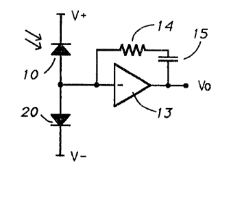
Fig. 3 illustrates an optical receiver in accordance with an
embodiment of this invention which enables this disadvantage of the
prior art to be avoided. In the optical receiver of Fig. 3, the
photodiode 10 is directly coupled to the transimpedance amplifier
comprising an a.c. coupled amplifier 13 and transimpedance resistor
14, the transimpedance resistor 14 being a.c. coupled to the output of
the amplifier 13 via a coupling capacitor 15. In contrast to the
prior art, in the optical receiver of Fig. 3 the photodiode 10 is
reverse biassed via a forward biassed diode 20. The diode 20
desirably has a small junction area to minimize its capacitance, and
maximize its impedance, particularly at low bias levels, and should
have a low reverse leakage. For example, the d;ode 20 may be a
silicon diode type lN914. Alternatively, and especially for high
speed applications, the diode 20 may be a p-i-n type diode having a
low capacitance, for example Hewlett Packard-Packard type 5082-3900.
The a.c. coupled amplifier 13 conveniently has a form such as
that described below with reference to Fig. 4. A d.c. coupled
amplifier, such as the amplifier 12 of the prior art, could be used
in the optical receiver of Fig. 3 with a.c. coupling of the junction
between the diodes 10 and 20 to the input of the transimpedance
amplifier, for example via the capacitor 18. However, the direct
coupling of Fig. 3 is preferred because it can be physically smaller
than a.c. coupling. This is significant because the virtual-ground
input of the transimpedance amplifier is very sensitive to
electro-magnetic interference, and because any stray capacitance
results in extra noise.
Referring to Fig. 4, the a.c. coupled amplifier 13
conveniently comprises an input field effect transistor 21, connected
in common-drain or source-follower mode, and a bipolar transistor 22
lZ99Z~5
connected in common-emitter mode, with a.c. coupling therebetween via
a capacitor ~3. Resistors connected between the collector-base and
base-emitter electrodes of the transistor 22 have high resistances
which are selected to bias the amplifier output at about mid-way
between the OV and 5V supply rails.
Referring again to Fig. 3, in the presence of an incoming
modulated light signal, the photodiode 10 generates a photocurrent
which flows through the diode 20, which acts as a load impedance for
the photodiode 10. The diode 20 has a small signal resistance which
is inversely proportional to the photocurrent, and the transimpedance
amplifier is designed to have a much lower input impedance.
Consequently, substantially all of the modulated signal current is
coupled to the input of the transimpedance amplifier, and flows to the
transimpedance resistor 14, rather than being lost in the load diode
20.
The load diode 20 contributes noise which is thermal noise
associated with the diode's small signal resistance. For a silicon
diode 20 such as that referred to above, having an ideality factor of
about 2, the mean square current noise is approximately equal to the
quantum shot noise associated with the photocurrent. Consequently,
the noise increase due to the presence of the load diode 20 is
relatively small, and the total noise present at the input of the
transimpedance amplifier is typically insignificant in comparison to
the thermal noise of the amplifier itself.
In contrast to the prior art, in the optical receiver of Fig.
3 the direct voltage which is dropped across the load impedance for
the photodiode 10, namely the diode 20, is limited to about 0.7 volt
even at the highest common photocurrent levels. In consequence, the
potential d;fference between the supply voltages V+ and V- can be
greatly reduced, to the order of 5 volts. This advantage is achieved
without compromising the dynamic range or noise levels of the optical
receiver.
As in the prior art, the photodiode 10 in the optical receiver
of Fig. 3 may be an avalanche photodiode especially for high frequency
modulating signals of the order of 600Mb/s or more, or may be a p-i-n
type photodiode, especially for these or lower frequency modulating
signals.
s
As is well known, the resistance of the transimpedance
resistor 14 should be high in order to achieve a high gain and low
noise. However, the supply voltage for the ampl;fier 13 must exceed,
with some margin, the product of peak-to-peak photocurrent with the
transimpedance resistance. For optimal results, typically the
quiescent bias level of the output of the amplifier 13 is designed, as
described above in relation to Fig. 4, to be close to the midpoint
between the power supply voltages V+ and V-. As the signal level
increases, it appears symmetrically about this bias level, the
coupling being a.c.
With b;nary digital modulating signals, a linear amplifier
characteristic is not essential, and signal compression is possible.
It is known to achieve such signal compression by providing a pair of
semiconductor diodes connected in parallel with one another and with
opposing polarities, in parallel with the transimpedance resistor 14.
However, the capacitance associated with such diodes causes a
frequency and level-dependent distortion of the signal to a degree
which may be unacceptable. In particular, where the transimpedance
resistor has a high resistance, for example 1 MQ, the capacitance of
the diodes degrades the frequency response of the optical receiver at
low signal levels.
Fig. 5 illustrates an optical receiver which provides signal
compression but which avoids this disadvantage. In the optical
receiver of Fig. 5, an impedance 24, for example comprising a 1kQ
resistor and a lnF capacitor in parallel with one another, is
connected between the load diode 20 and the negative supply voltage
V-. The relatively small resistance of the impedance 24 is such that
the voltage drop across this resistor is much less than l volt even at
the highest photocurrent levels. In this optical receiver, signal
compression is provided by a pair of oppositely poled diodes 25 and
26, connected in parallel with one another, a.c. coupled via a
capacitor 27 between the output of the amplifier 13 and the junction
between the load diode 20 and the impedance 24.
At low signal levels, the signal compression diodes 25 and 26
are substantially capacitive, but they are isolated from the input
node of the transimpedance amplifier by the load diode 20, which has a
relatively high impedance at high signal levels. In addition, the
lZ9~Z~5
impedance 24 forms with the signal compression diodes 25 and 26 a
potential divider, which due to the low magnitude of the impedance 24
greatly attenuates the level of the output voltage Vo which is fed
back towards the input of the transimpedance amplifier. Consequently,
the optical receiver of Fig. 5 avoids the capacitive feedback problems
of the known signal compression arrangements discussed above.
At high signal levels, at which the load diode 20 has a
relatively low impedance, the output voltage Vo drives the diodes 25
and 26 into conduction at the instantaneous extreme signal levels, and
current flows back into the virtual ground at the input node of the
transimpedance amplifier via the diode 20. The optical receiver thus
provides a considerable dynamic range. With a potential difference of
5 volts between the supply voltages V+ and V-, the compressed output
signal level Vo is typically of the order of 0.5 volt peak-to-peak.
Fig. 6 illustrates a further form of optical receiver which is
similar to that of Fig. 3, except that the transimpedance resistor 14
and coupling capacitor 15 are replaced by a capacitor 28. The
capacitor 28 has a capacitance which is small in relation to the
capacitance of the photodiode 10 and the input capacitance of the
amplifier 13 in order not significantly to degrade the noise
performance of the optical receiver, especially at high frequencies.
Assuming that the amplifier 13 has a conventional single pole open
loop characteristic, the input impedance of the transimpedance
amplifier with the capacitive feedback provided by the capacitor 28 is
resistive. As indicated above, th;s input impedance is designed to be
much less than the small signal resistance of the load diode 20.
As the transimpedance amplifier in the optical receiver of
Fig. 6 has only capacitive feedback, the feedback element generates no
noise. The resistive noise contribution, which is typically dominant,
of conventional transimpedance amplifiers having resistive feedback is
thereby avoided, resulting in improved sensitivity of the Dptical
receiver. In addition, a transimpedance amplifier having capacitive
feedback as shown in Fig. 6 is relatively stable and can be relatively
easily manufactured.
The capacitor 28 can typically have a capacitance which is
less than lpF, enabling the transimpedance amplifier to have a high
lZ99245
gain. This gain is frequency dependent, rolling off linearly with
increasing frequency. If a flat response is desired, the optical
receiver output signal voltage Vo can be coupled via an equalization
stage, such as a differentiator, having a frequency dependent gain.
However, such an equalization stage is unnecessary in an optical
receiver arrangement as described below with reference to Fig. 8
or 9.
Instead of providing the capacitor 28 as a transimpedance
element, the capacitance of the photodiode 10 itself may be used by
connecting the photodiode 10 in the feedback path of the amplifier 13.
Figs. 7 and 8 illustrate optical receivers in which this is done.
Referring to Fig. 7, the photodiode 10 reverse biassed from a
-5 volt supply via the forward biassed diode 20, is a.c. coupled in
the feedback path of the amplifier 13 by the coupling capacitor 15 and
a potential divider constituted by resistors 30 and 31, the photodiode
10, resistor 30, and capacitor 15 being connected in series between
the inverting input and the output of the amplifier 13, and the
resistor 31 being connected between a zero volt supply line and the
junction between the photodiode 10 and the resistor 30.
The capacitor 15 serves to block d.c., and has a capacitance
which is very much greater than that of the photodiode 10. The
potential divider attenuates the output of the amplifier 13 by a
factor of for example about 5 determined by the ratio of the
resistances of the resistors 30 and 31 (for example 500 and 100 ohms
respectively), whereby the effective capacitance of the
transimpedance circuit is equal to the capacitance of the photodiode
10 divided by this factor. The attenuator thus avoids too high an
effective capacitance in the feedback path, and hence too low a gain
of the transimpedance amplifier. With a low capacitance of the
photodiode 10 it is conceivable that the attenuator ~resistors 30 and
31) could be omitted.
In the optical receiver of Fig. 7, the resistors 30 and 31
introduce a noise component which is undesirable. This is avoided by
the alternative arrangement of Fig. 8, in which the attenuator is
formed by a capacitive potential divider comprising capacitors 30' and
31'. The capacitors 30' and 31' can have capacitances of for example
10pF and 50pF respectively, to prov;de the same attenuation factor of
lZ9~Z~5
about 5 as in the optical receiver of Fig. 7. In view of this
capacitive coupling, in the optical receiver of Fig. 8 the coupling
capacitor 15 of Fig. 7 is not required, but a resistor 29 is provided
in parallel with the capacitor 31' to provide a d.c. path for the
photodiode 10. The resistor 29 is selected to have a resistance which
is high compared with the impedance of the capacitor 31' which shunts
it, whereby its noise contribution is also shunted and thereby
reduced, but which is not so high that it overly restricts the dynamic
range of the optical receiver.
The same comments, regarding the frequency dependence of gain,
apply to the optical receivers of Figs. 7 and 8 as to the optical
receiver of Fig. 6, because these optical receivers also have a
capacitive transimpedance element.
In an optical receiver arrangement, the output signal from an
optical receiver is typically coupled via a filter which is designed
to maximize the "eye" opening while minimizing noise by restricting
bandwidth. Such a filter desirably is a matched filter having a sinc
((sine x)/x) response, augmented by a low-pass filter for removing
noise from second and subsequent lobes of the sinc filter. Fig. 9
illustrates a sine filter which is particularly suited for such
purposes when used with the optical receiver of F;g. 6, 7, or 8.
Referring to Fig. 9, the filter illustrated therein comprises
an NPN bipolar transistor 32, having a base for receiving an input
voltage Vin, a collector for supplying an output signal voltage Vout,
coupled to a positive supply voltage of 5 volts via a collector
resistor 34, and an emitter coupled via resistors 36 and 38 to a zero
voltage supply rail. In addition, the filter cornprises an open
circuit transmission line 40, one end of which is coupled across the
resistor 38. The transmission line 40 may comprise a coaxial cable,
stripline, or any other form of transmission line suitable for
providing a delay as described below. The resistor 36 couples the
emitter of the transistor 32 to the transmission line 40 in a matched
manner. To this end the resistance of the resistor 36, plus the
output impedance at the emitter of the transistor 32, in parallel with
the typically much greater resistance of the resistor 38, is selected
to equal the characteristic impedance of the transmission line 40, for
example 50 ohms. For example, the output impedance of the transistor
~9Z45
12
may be of the order of lO ohms, and the resistors 36 and 38 may have
resistances of the order of 40 ohms and 1000 ohms respectively. The
resistor 34 may conveniently have a resistance of the order of 50
ohms.
The transmission line 40 is selected to have a length which is
such that the signal propagation delay along the transmission line
from its connected end to its open circuit end is equal to half the
bit period T of a binary digital signal to be filtered? whereby the
round-trip transmission delay along the line 40 and back is equal to
the bit period T. For a signal with a bit rate of 600 Megabits per
second the length of the transmission line 40 would be typically about
17 centimeters. A signal appearing in the emitter circuit of the
transistor 32 is reflected by the open circuit end of the transmission
line 40, whereby the filter provides a sine (~T/2) response.
Fig. lO illustrates an alternative form of sine filter, which
is similar to that of Fig. 9 except that the resistor 38 is dispensed
with, and a constant current circuit 39 is connected between the
emitter of the transistor 32 and the zero volt supply line. Again in
this case, the resistor 36 provides a matched coupling of the emitter
of the transistor 32 to the line 40.
Fig. 11 illustrates a further alternative form of sine filter
which is at present preferred. The filter of Fig. 11 substitutes the
resistor 38 for the constant current source 39 of the filter of Fig.
10, and provides a differential output voltage Vo taken from the
collector of the transistor 32 with respect to the collector of
another transistor 32', whose base is supplied with the input signal
Vin and which has collector and emitter resistors 34' and 38', but no
transmission line associated therewith. The differential output and
the components 32', 34', and 38' serve to eliminate from the output
voltage Vo effects arising from the resistor 38 and any capacitance at
the emitters of the transistors.
The optimum filter has a response of the form sine
(~T/2)/(~T/2), which can be achieved by cascading the sine filter of
Fig. 9, 10, or 11 with an integrating stage which supplies the inverse
frequency dependent response of 2/~T. However, the optical receiver
of Fig. 6, 7, or 8 already provides such an integrating function, so
that the circuits of Fig. 6, 7, or 8 and Fig. 9, 10 or 11, can be
~ 2~45
directly cascaded to provide the optimum response without having
either a differentiator for compensating for the response of the
optical receiver or an integrator for complement;ng the response of
the sine filter.
Fig. 12 illustrates in a block diagram an optical receiver
arrangement which comprises such cascaded circuits. In Fig. 12, an
optical receiver 42, which is as described above with reference to
Fig. 6, 7, or 8, has its output coupled directly to a filter 44, which
is as described above with reference to Fig. 9, 10, or 11. The output
Vout of the filter 44 is coupled via a low-pass filter 46 to a digital
comparator 48, from which a recovered binary digital signal is derived
in known manner. The low-pass filter 46, which can have a cut-off
frequency approximately equal to the bit rate of the digital signal,
e.g. 600MHz for a digital signal having a bit rate of 600Mb/s, serves
to restrict noise levels to those contributed substantially only
within the first lobe of the sine filter of Fig. 9, 10, or 11, as
described above. The design of this low-pass filter 46 is not
particularly critical, and it can alternatively be between the optical
receiver 42 and the filter 44 or incorporated within either of these
circuits. The optical receiver arrangement may further include
addit;onal amplification and/or a.g.c. stages which may be provided in
any desired location between the output of the optical receiver 42 and
the input of the comparator 48.
Fig. 13 illustrates an optical receiver in accordance with
another embodiment of the invention, which can be used in place of the
optical receiver of Fig. 6, 7, or 8, with the sine filter of Fig. 9,
10, or 11 and the optical receiver arrangement of Fig. 12. As
illustrated in Fig. 13, this optical receiver is substantially the
same as that of Fig. 6 except that the photodiode 10 is biassed in the
conventional manner via the load resistor 16 as in the prior art of
Fig. 2.
Although embodiments of the invention have been described
above in detail, it should be appreciated that numerous modifications,
adaptations, and variations may be made thereto without departing from
the scope of the invention as defined in the claims.