Note: Descriptions are shown in the official language in which they were submitted.
~Z99~8
Frequency converter
___ __ _____
Back~round of the I_v_ntion
Field of the Invention
__ _ ___________ ._
This invention relates to a frequency converter, and
more particularly to a frequency converter suitable for a
multi-channel broadcast signal receiver.
Descri~tion of the Prior Art
______ _ _ _____ _ __ ___
Generally, the basic function of a frequency converter
is to convert frequencies of received broadcast signals
into prescribed frequencies. In this frequency conversion
operation, although it is necessary to take a sufficient
signal-to-noise ratio (S~N) into account to obtain the
required power gain, the frequency conversion operation
must be performed that a prescribed selectivity can be
maintained. Also, to avoid signal distortion, such as
cross-modulation distortion, the gain of the frequency
converter must be controlled. However, it has been
difficult to eliminate the signal distortion and improve
the S/N simultaneously since an improvement in one results
in a degradation of the other. Therefore, the prior art
faced a problem of how to suppress the signal distortion
and prevent a simultaneous deterioration of the S/N of the
frequency converter.
lZ9~Z4~
-- 2 --
Apart from receivers for conventional television
broadcasting, this problem also affects receivers for CATV
broadcasting, which is a multi-channel broadcasting with
many transmission channels.
In a CATV converter which functions as a tuner-
converter for a CATV receiver, channel frequencies, i.e.,
first-RF signal frequencies of received CATV broadcast
signals, are first converted into corresponding second-RF
signal frequencies which are higher than the first-RF
signal frequencies of the received CATV broadcast signals
by a first mixer (up conversion) and then selectged by a
second-RF tuned amplifier and converted into a prescribed
television channel frequency representing a vacant channel
(non-broadcast channel) among a general television broad-
cast channel band, e.g., the VHF band, or the UHF band by
a second mixer (down conversion). This type of frequency
converter is known as an up-down frequency converter
because it first converts the first-RF signal frequency
into the second-RF frequency which is higher than the
first-RF signal frequency and then converts the second-RF
frequency into the prescribed television channel frequency
which is lower than the first-RF signal frequency.
The frequency conversion as described above is carried
out on the respective multiple CATV broadcast signals,
while the received CATV broadcast signals or the first-RF
signals are transmitted through a coaxial cable and applied
to the frequency converter. Levels or intensities of
individual channel signals of the CATV broadcast channels
band are not always the same. Therefore, a tilt amplifi-
cation characteristic can be employed at a line repeater
which is provided in a transmission line for a reception
terminal, i.e., the frequency converter, to make its gain
vary for the lower and higher transmission channel
frequencies. The tilt amplification characteristic of the
line repeater is determined by responding to level
deviations among channels in the reception terminal, signal
~299z~a~
distortion in the transmission system, etc. That is to
say, the transmission characteristics of the tilt ampli-
fication characteristic of the line repeater should be
determined by taking into account the signal distortion
and the S/N of frequency converter in the reception
terminal.
To enable the prior art to be described with the aid
of diagrams, the figures of the drawings will first be
listed.
Figure 1 is a circuit diagram showing an embodiment of
the frequency converter according to the present invention;
Figure 2 is a graph illustrating the GR to AGC voltage
characteristics;
Figure 3 is a graph illustrating the NF to GR
characteristics;
Figure 4 is a graph illustrating the second order
distortion to GR characteristic;
Figure 5 is a graph illustrating the cross-modulation
distortion to GR characteristic; and
Figures 6 and 7 are circuit diagrams showing
conventional circuits.
Figure 6 shows a circuit of a conventional up-down
frequency converter. In the figure, a plurality of CATV
broadcast channel signals are applied to an input terminal
1. Then plurality of CATV broadcast channel signals are
inputted to a first mixer 4 via a band pass filter (BPF)
which comprises of a high pass filter ~HPF) 2 and a low
pass filter (LPF) 3. First mixer 4 also has applied an
output of a first local oscillator 6 via an amplifier 5.
The frequencies of the input CATV broadcast signals are
raised in first mixer 4, respectively, to frequencies each
higher by a first oscillation frequency of first local
oscillator 6. The frequency-converted signals, i.e.,
second-RF signals from first mixer 4 are input to second
mixer 10 via a first frequency gate which comprises a BPF
7, a second-RF signal amplifier 8 and a BPF 9. The first
9Z~8
-- 4
frequency gate passes through it a signal with a prescribed
second-RF frequency of the second-RF signals to second
mixer 10. Second mixer 10 receives the output of a second
local oscillator 11. Second mixer 10 lowers the prescribed
second-RF frequency of the signal that passed through the
first frequency gate to a prescribed frequency which
corresponds to a vacant channel (non-broadcast channel)
among the aforementioned conventional television broadcast
channel band, e.g., the VHF band or the UHF band, in using
the oscillation output of second local oscillator 11.
The frequency-converter signal is output from OUtpllt
terminal 13 via output BPF 12.
As described above, it is generally desirable that the
frequency converter should not deteriorate its noise figure
(NF) characteristics and should suppress any signal
dis~ortion occuring therein.
When a non-linear signal distortion occurs in an
amplifier, generally there is a following relationship
between an input signal voltage and an output voltage of
the amplifier.
m
Ye = ~ Kn-en ... (1)
n=l
wherein,
Ye : Output signal voltage of amplifier
e : Input signal voltage of amplifier
Kn : Coefficient presenting a linearity of
amplification the amplifier
n : Order of signal distortion
Although the non-linear signal distortion occurs to
fairly high orders as seen from Equation (1), only the
second order distortion component (n = 2) and the third
order distortion component (n = 3) need to be considered
for practical use. When the amount of the signal
distortion given by Equation (1) rises in an amplifier
~. .
~zg92~8
-- 5 --
constituting the frequency converter, a cross-modulation
disturbance and a beat disturbance occur. The degree of
the cross-modulation disturbance is proportional to the
square of ~he amplitude of the signal which interferes
with the desired signal. Moreover, the cross-modulation
disturbance becomes greater as number of the received
broadcast channel signals increases.
On the other hand, the beat disturbance occurs when
signal distortions occurring for a plurality of the
received broadcast channel signals are present in the
television broadcast channel bandO For reducing the
effect of the cross-modulation distortion and the beat
disturbance, pre-amplifier 14 could be removed from the
circuit arrangement shown in Figure 6. However, then a
carrier-to-noise ratio (C/N) at the frequency converter
worsens, due to the lack of the pre-amplifier.
The C/N is generally expressed by
C/N[dB] = ei[dB u] - NF[dB] - 0.8[dB] . . (2)
Also, a total amount of the C/N is given as follows:
C/Nm[dB] = C/N[dB] - 10 logl0 m[dB] ......... (3)
wherein m represents the number of amplifier stages
connected in cascade. As seen from Equation (3), the total
amount of the C/N, i.e., the C/Nm, is inversely
proportional to the number of amplifier stages in cascade;
m. In other words, when m number of amplifier stages of
the same performance are connected in cascade, the C/N of
the frequency converter worsens by 10 logl0 m[dB].
Therefore, when m number of amplifier stages are connected
~ in cascade, each amplifier stage requires for its input
signal a level of ei, given in the following Equation
~4), in order to maintain the C/N in value the same as
when only one amplifier stage is used.
~zg9z~8
ei[dB u] = emin[dB u] + 10 logl0 m .. (4)
wherein emin represents the lowest signal input level
which is obtained using ~quation (2).
It is clear from Equation (4) that, in order to obtain
the C/N over a prescribed value, the input signal is
required to be at a sufficient level over a prescribed
level.
Therefore, the input signal level for the frequency
converter must be set to an optimum level to satisfy both
requirements of low signal distortions and high C/N.
In the conventional frequency converter shown in Figure
6, since no pre-amplifier is provided prior to first mixer
4, although a lower processed signal level is desirable for
reducing the signal distortion, the C/N is deteriorated
since the input signal level is insufficient to satisfy the
prescribed C/N required in the rear stage amplifier, e.g.,
second-RF amplifier 8.
For resolving the problem, a pre-amplifier is provided
prior to the first mixer, for example, in a position
between HPF 2 and LPF 3 which are shown in the Figure 6.
This pre-amplifier is employed at the cost of increasing
the signal distortion, such as the cross-modulation
distortion. Figure 7 is a circuit diagram showing the
construction of this type of circuit, and it differs from
the circuit in Figure 6 in that amplifier 14 is provided.
Amplifier 14 is generally called a pre-amplifier. It is
provided for preventing the deterioration of the C/N of
the frequency converter.
In the frequency converter shown in Figure 7, pre-
amplifier 14 amplifies the input signal to a required
level, given by Equation (4), and contributes to the
obtaining of the prescribed C/N. On the other hand, the
second and the third order distortions are increased.
129g~48
That is to say, although the C/N is improved, cross-
modulation distortion will occur if there is non-linear
distortion in pre-amplifier 14. Thus it is necessary to
control the gain of pre-amplifier 14 so that the signal
distortion is not increased by excessive gain.
~hen an m number of amplifier stages are connected in
cascade, if power gains of the respective amplifier stages
are taken as Gl, G2, ... Gm and the NFs of the respective
amplifier stages are taken as NFl, NF2, ~.~ NFm, the total
noise figure NFt is expressed by
Gl Gl^G2 - Gl G2--- Gm-l (5)
Thus for improving the NF and the C/N, it is
advantageous to heighten the gain of the amplifiers in the
rear stages of the frequency converter. On the other hand,
for suppressing the signal distortion, it is desirable to
heighten the gain of the amplifiers in the front stages of
the frequency converter. Therefore, with respect to the
gains of the amplifiers, the NF or the C/N characteristic
of its frequency converter and the signal distortion
characteristic have responses inconsistent with each other.
In the conventional frequency converter as shown in
Figure 7, either pre-amplifier 14 or second-RF amplifier 8
is made so that its gain may be controlled automatically
in response to the output of the frequency converter.
That is, an automatic gain control (AGC) is performed in
one of pre-amplifier 14 or second-RF amplifier 8~
If the AGC is carried out in second-RF amplifier 8, a
sufficient level of the input signal must be maintained
over the level which satisfies Equation (4), so that the
C/N will not be excessively deteriorated. However, signal
distortion becomes severe when the level of the input
signal exceeds a predetermined level in conjunction with
the AGC. This is because the AGC is carried out for the
signal from first mixer 4, in which the signal distortion
~z~9z~
-- 8 --
has occurred due to non-linear characteristic elements of
first mixer 4 for effecting the frequency conversion.
Moreover, in the case when the AGC is carried out in
pre-amplifier 14, there is a limit to the extent of gain
reduction (GR) due to the AGC, because pre-amplifier 14
is, for example, a 55-450 MHz broad band amplifier.
Thus the GR for pre-amplifier 14 cannot be expected to
sufficiently suppress the signal distortion.
Thus, in the conventional frequency converters shown
in Figures 6 and 7, since both the C/N characteristic and
the distortion characteristic are prescribed, recently
there has been a problem in that it is difficult to control
the signal gain for those levels.
Summary of the Invention
__ _________
An object of the present invention is to provide a
frequency converter which can control the signal level at
an optimum value suitable for both the C/N characteristic
and the signal distortion characteristic.
These and other objects are achieved in a frequency
converter comprising: an input terminal for receiving a
broadcast signal with a first frequency; a first variable
gain amplifier for amplifying said broadcast signal applied
from said input terminal comprising a first transistor
connected in a grounded emitter configuration and a second
transistor connected in a grounded base configuration; a
local oscillator for generating a local oscillation signal;
a frequency mixer circuit for converting said first
frequency of said broadcast signal applied from said first
variable gain amplifier to a second frequency using said
local oscillation signal output from said local oscillator;
a second variable gain amplifier for amplifying a signal
with said second frequency applied from said frequency
mixer circuit; and an AGC circuit means for feeding back to
said first and second variable gain amplifiers an AGC
signal which is obtained from a signal output from said
second variable gain amplifier.
~z~g~
- 9 -
Descri~tion of the Preferred Embodiments
_ ____ ____________________________ _
Embodiments of the present invention will now be
described in detail with reference to the accompanying
drawings, namely, Figures 1 to 5.
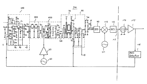
Referring now to Figure 1, there is shown the circuit
diagram of a frequency converter according to the present
invention. The circuit diagram shows an example of a
circuit which carries out the AGC for an up-down frequency
converter which receives multi-channel broadcast signals,
for example, CATV broadcast signals.
In Figure 1, a plurality of broadcast signals, e.g. r
the CATV broadcast channel signals are input to an input
terminal 100. Then the plurality of CATV broadcast channel
signals are applied from input terminal 100 to a first
mixer 400 via a first signal transmission circuit. The
first signal transmission circuit comprises of an HPF 200,
a pre-amplifier 140 and a LPF 300. First mixer 400 also
receives an oscillation output of a first local oscillator
60 via an amplifier 50. The input CATV broadcast channel
signals have their frequencies raised in first mixer 400,
respectively, to frequencies each higher by the first local
oscillation output of first local oscillator 60. The
frequency-converted signals, i.e.l second-RF signals, from
first mixer 400 are input to a second mixer 110 via a
second-RF signal tuner circuit 500 which comprises a BPF
70, a second-RF signal amplifier 80 and a BPF 90. The
second-RF signal amplifier 500 passes through it a signal
with a prescribed second-RF frequency of the second-RF
signals to second mixer 110. Second mixer 110 is supplied
with an oscillation output of a second local oscillator
111. Second mixer 110 lowers the prescribed second-RF
frequency of the signal that passed through second-RF
signal amplifier 500 to a prescribed frequency which
corresponds to a vacant channel (non-broadcast channel) of
the aforementioned conventional television broadcast
~zggz~
-- 10 --
channel band, e.g., the VHF band or the UHF band, in using
the oscillation output of second local oscillator 111.
The frequency-converted signal is output from output
terminal 113 via an output BPF 112.
In amplifier 140, transistors Ql and Q2 are connected
in cascade. Transistor Ql is connected in a grounded-
emitter configuration amplifier, while transistor Q2 is
connected in a grounded-base configuration amplifier.
An output circuit of the amplifier of transistor Ql is
connected to an input circuit of the amplifier of
transistor Q2 so that an input capacitance of the amplifier
of transistor Q2 is reduced. This makes the amplification
characteristic of the cascade connected amplifier flat over
a broad band. The broad band amplification is enhanced by
feeding back an output of transistor Q2 to the input
circuit of Ql via a feedback circuit composed of capacitors
Cl and C2 and a resistor R1. The feedback operation
carries out a broad band compensation. A series circuit
composed of a capacitor C5 and a resistor R7 is connected
between the collector of transistor Ql and a ground for
preventing an undesired oscillation in the cascade
connection amplifier. Moreover, base bias voltages for
transistors Ql and Q2 are applied by dividing a power
supply voltage +B with a series circuit of resistors R2,
R3 and R4 connected between a power supply terminal and
the ground potential circuit. For the collector of
transistor Q2, the bias voltage is applied via a choke
coil Ll which prevents undesired high-frequency signals
from getting into the bias circuit. The undesired
high-frequency signals are by-passed via a capacitor C3
connected between the bias circuit and the ground
potential circuit.
The output of pre-amplifier 140, composed of the
cascade amplifier of transistors Ql and Q2, is applied to
first mixer 400 via LPF 300 after its DC current component
~Z~9~4~
has been eliminated by a coupling capacitor C4 connected
in series with the output circuit o~ the grounded-base
configuration amplifier of transistor Q2.
Resistors R4, R5 and R6, which are connected ~o the
output side of pre-amplifier 140, essentially compose a
~ (pi)-network attenuator for an AC signal and contribute
to suppress the signal distortion that would occur in
following stage first mixer 400 due to non-linear
characteristic elements for a frequency conversion at first
mixer 400. The suppression of the signal distortion is
further ensured by means of following stage LPF 300, which
prevents the undesired high-frequency signal from getting
into first mixer 400.
In addition, pre-amplifier 140 has an AGC terminal Pl
for receiving an AGC signal, which will be explained in
detail later.
The frequency conversion at first mixer 400 is
effected by an addition of the broadcast signal (first-RF
signal) and the first local oscillation signal at a diode
bridge composed of diodes D10, D20, D30 and D40. The
first-RF signals are applied to the diode bridge through
transformers T10 and T20 which are connected in series with
an input circuit of first mixer 400. The first local
oscillation sig:nal is applied to the diode bridge through
a tap of a secondary winding of transformer T20. The
second-RF signals thus converted by the diode bridge are
output through a BPF composed of a transformer T30, an
inductor L10, and capacitors C10 and C20 in first mixer
400. The second-RF signals output from first mixer 400 are
applied to second-RF tuner circuit 500 composed of BPF 70,
second-RF signal amplifier 80 and BPF 90 as described
above.
Second-RF tuner circuit 500 has a prescribed tuning
frequency, i.e, a prescribed second-RF signal frequency,
which corresponds to a desired CATV broadcast channel
~z9~
- 12 -
frequency so that only the prescribed second-RF signal is
effectively transmitted therethrough. BPF 70 is of a ~/4
type composition with a steep band pass filtering
characteristic. Therefore, sPF 70 selects a signal having
the tuning frequency, i.e., the prescribed second-RF signal
frequency among the plurality of the second-RF signals from
first mixer 400. The prescribed second RF signal thus
selected is amplified in second-RF signal amplifier 80.
The selection of the prescribed second-RF signal is most
effected by BPF 90.
Second-RF signal amplifier 80 is composed of an FET
Q3 in order to suppress the third order distortion. The
signal, i.e., the prescribed second-RF signal applied
thereto, has been amplified in pre-amplifier 140 to the
level such that the C/N of the signal is not deteriorated
as expressed in Equation (4). Moreover, second-RF signal
amplifier 80 has an AGC terminal P2 for receiving the AGC
signal. That is, F~T Q3 receives the AGC signal at its
second gate G2 so that the gain of second-RF signal
amplifier 80 is controlled. The gain reduction (GR) in
second-RF signal amplifier 80 due to the AGC is made
greater than the GR in pre-amplifier 140 for improving
the NF and the C/N in the frequency converter. This is
because a greater GR in second stage amplifier is
advantageous for improving the NF and the C/N when compared
to the GR in the first stage amplifier, as aforementioned
and seen from Equation (5). ~oreover, the greater GR in
second-RF signal amplifier 80 is necessary for suppressing
the cross-modulation distortion which would occur at
another frequency conversion in the second mixer 110.
The gain controlled output signal from second-RF
signal amplifier 80 is input to BPF 90 via a filter
composed of a transformer T40, which is of also a ~/4 type
composition with a steep band pass filtering characteristic
due to inductive coupling, and then via an impedance
~Z99Z~
- 13 -
matching circuit composed of indu~tors L20 and L30 and a
capacitor C30. The prescribed second-RF fre~uency signal
from second-RF signal amplifier 80 has the undesired
frequency components ~urther reduced by the filter
composed of transformer T40 and BPF 90, so that the
selectivity for the prescribed second-RF frequency signal
is sufficiently raised.
In second mixer 110, the prescribed second-RF
frequency signal is lowered in frequency to the prescribed
frequency which corresponds to the prescribed channel of
the conventional television broadcast channel as mentioned
above, in using the second local oscillation output of
second local oscillator 111. The prescribed television
channel frequency signal thus converted is applied to a
television receiver through output terminal 113 of the
frequency converter. In the television receiver, the
prescribed television channel frequency signal from the
frequency converter is again lowered in frequency to an
intermediate frequency (IF) in the normal manner. The IF
signal is applied to an AGC signal detection circuit 116
through a surface wave filter 114 and an IF signal ampli-
fier 115. Surface wave filter 114 rises the selectivity
for the prescribed IF signal by its steep band pass
filtering characteristic, while IF signal amplifier 115
amplifies the IF signal.
In AGC detection circuit 116, an AGC signal is
detected from the IF signal by well-known technique, for
example, a peak detection which detects signal peaks.
The AGC signal thus detected is supplied simultaneously to
30 AGC terminals Pl and P2 of pre-amplifier 140 and second-RF
signal amplifier 80 so that an AGC loop is formed.
The AGC in the frequency converter shown in Figure 1
will be now explained in detail. The frequency conversion
is carried out by means of a heterodyne operation in first
35 mixer 400. For suppressing the signal distortion which
~g~Z~
- 14 -
occurs due to non-linear characteristic elements for the
frequency conversion, the diode bridge comprised of diodes
D10, D20, D30 and D40 is, for example, employed in first
mixer 400 as described above. However, the frequency
conversion is accompanied by a conversion loss, so that
the signal to be supplied to second-RF signal amplifier
circuit 80 becomes insufficient to prevent the C/N from
being severely deteriorated.
Therefore, pre-amplifier 140 is provided in front of
first mixer 400 in order to make the C/N no worse than the
C/N of the received signal on input terminal 100. However,
if the gain of amplifier 140 exceeds a predetermined value,
the signal distortion as obtained by Equation (1) will
increase over a predetermined value due to the non-
linearity of amplifier 140 itself.
As is well-known, the non-linearity of the amplifier
itself gives rise to undesired high-frequency signals,
cross-modulation distortion signals etc. The undesired
high-frequency signals, cross-modulation distortion
signals etc. then interfere with the desired signal.
The non-linear distortion creates a serious problem when
there are a plurality of broadcast channels such as the
conventional television broadcast channel waves or the
CATV broadcast channel waves.
Therefore, it is necessary for the gain of pre-
amplifier 140 to be controlled to a degree such that the
non-linear distortion is below an acceptable low level,
and also to have the gain such that the C/N will not be
badly deteriorated in processing the signals in the
following stage. For that purpose, pre-amplifier 140 is
provided an AGC terminal Pl so that its gain is controlled
to an optimum degree to not worsen the non-linear
distortion below the acceptable level.
In the cascade amplifier of pre-amplifier 140, the
grounded-emitter configuration amplifier composed of
--.
~Z99248
- 15 -
transistor Ql is further provided an impedance circuit,
such as is well-known. The impedance circuit is comprised
of a DC impedance circuit and an AC impedance circuit
respectively for establishing prescribed DC and AC emitter
biases for the emitter of transistor Ql. The DC impedance
circuit comprises resistors R51 and R52 connected in series
between the e~itter of transistor Ql and the ground
potential circuit, while the AC impedance circuit comprises
capacitors C50, C60 and C70 connected in series between the
emitter of transistor Ql and the ground potential circuit.
In addition, the AC impedance circuit is provided a diode,
for example, a PIN diode D50, connected in series between
capacitors C60 and C70 at a forward bias condition. Then
the aforementioned AGC terminal Pl is connected to the
anode of PIN diode D50.
The gain of the grounded-emitter configuration ampli-
fier composed of transistor Ql which composes the cascade
amplifier is controlled in accordance with the emitter
impedance. On the other hand, the capacitive impedance of
PIN diode D50 is variable in accordance with the forward
bias applied thereon. Therefore, PIN diode D50 can vary
the emitter impedance in response to the AGC signal applied
to AGC terminal Pl so that the AGC for pre-amplifier 140 is
established. When the maximum AGC signal is applied to AGC
terminal Pl, it is assumed here that the gain reduction in
pre-amplifier cannot be achieved (GR = 0 dB).
On the other hand, the gain reduction due to the AGC
is carried out by decreasing the AGC signal so that the AC
impedance on the emitter of transistor Ql is increased.
By the action of the AGC, the gain of pre-amplifier 140 is
reduced to the optimum value and the signal distortion due
to amplifier 140 is suppressed.
The AGC, in combination with the capacitive AC
impedance circuit to the emitter of transistor Ql, is
effective for suppressing the non-linear distortion which
i29~2~
- 16 -
occurs in pre-amplifier 140 itself. Moreover, since the
optimum gain adjustment is carried out at a stage prior to
first mixer 140, which is composed of diodes D10, D20, D30
and D40 which are the non-linear characteristic elements,
the deterioration of the NF expressed by Equation (5) can
be controlled to not worsen below an acceptable level.
Furthermore, the AGC for pre-amplifier 140 is effective
for compensating in advance the conversion loss in the
first mixer 400. Therefore, second-RF signal amplifier
circuit 80 is able to amplify the prescribed second-RF
signal to a level ensuring the C/N over a predetermined
degree but without increasing the cross-modulation
distortion over the acceptable degree.
The AGC for second-RF signal amplifier 80 will now be
described in detail. The AGC is performed by applying the
AGC signal to second gate G2 of FET Q3 in second-RF signal
amplifier 80. The AGC signal alters the bias voltage of
second gate G2 of FET Q3 so that the gain of second-RF
signal amplifier 80 is controlled.
FET Q3 itself generates a small amount of third order
distortion so that the cross-modulation distortion can be
made smaller in second mixer 110. As expressed in Equation
(5), from the viewpoint of prevention of deterioration of
the NF, it is desirable that the rear stage amplifier
perform a greater gain reduction compared to the first
stage amplifier. In this sense, the gain reduction (GR)
of second-RF amplifier 80 is made greater than the gain
reduction of pre-amplifier 140.
The non-linear distortion in an amplifier as given by
Equation (1) will now be investigated in detail. As
described before, the third order distortions in the non-
linear distortions become problems in practical use.
In the third order distortion, there are included the
cross-modulation distortion with a frequency the same as
the frequency of the input signal and a beat with a
i~g9~
frequency different from the frequency of the input signalJ
In the second order distortion, it includes the beat but
does not include the cross-modulation distortion with the
frequency of the input signal.
If the cross-modulation distortion occurs, the desired
channel signal is modulated by signals in other channels,
so that the quality of the reproduced picture on television
receivers will be seriously deteriorated. If the beat
occurs, so-called beat stripes appear on the television
receivers, so that the reproduced picture will be also
seriously deteriorated.
In the embodiment shown in Figure 1, the control of
the gain reduction is carried out on both amplifier 140 and
amplifier 80 by the same AGC signal. Therefore, the
frequency converter is protected from the deterioration of
the NF and the C/N and also from the disturbances of beat
and cross-modulation distortion.
Figure 2 shows the gain reduction control character-
istics for the AGC signal in the embodiment of Figure 1.
In Figure 2, graph A shows the GR characteristic at pre-
amplifier 140, graph B shows the GR characteristic at
second-RF signal amplifier 80 and graph C shows the total
GR characteristic of the frequency converter. As is clear
from Figure 2, a particular state that the GR = O(dB)
corresponds to the AGC signal of about 9(V). And as the
AGC signal reduces, the GR graphs A, B and C increase.
As is also clear from Figure 2, the GR graph A for pre-
amplifier 140 is less than the GR graph B for second-RF
signal amplifier 80. The relation of the graphs A and B
serves to simultaneously prevent the deterioration of the
NF and the C/N and the disturbances from the beat and the
cross-modulation distortion. That is, it is desirable to
carry out gain reduction in the rear stage second-RF signal
amplifier 80 rather than to reduce the gain as much as
possible in the front stage pre-amplifier 140, in order to
~29~
amplify the input signal withou~ causing the deterioratiGn
of the NF and the C/N. On the other handl the gain of the
pre-amplifier 140 is determined by taking into account the
optimum signal level required for the advance compensation
of the conversion loss in the frequency conversion at first
mixer without increasing the non-linear distortion over the
acceptable degree.
In second-RF signal amplifier 80, the deterioration of
the NF and the C/N are less even though the GR is made
greater. Therefore, the GR of second-RF signal amplifier
80 is controlled to the optimum for minimizing the
distortions due to the frequency conversion in the rear
stage second mixer 110. In this case, the GR is controlled
to a degree which does not fall below the level required in
the rear stage circuit (e.g., amplifier 114 in the tele-
vision receiver outside the frequency converter) in accord-
ance with Equation (4) in order not to suppress the
deterioration of the C/N of the whole frequency converter.
This type of optimum GR value control characteristic for
the frequency converter as a whole is shown by graph C in
Figure 2.
Figure 3 is a characteristic diagram showing relation-
ships of the noise figure NF to the gain reduction GR of
the embodiment of Figure 1. Graphs A, B and C in Figure 3
also designate the characteristics of pre-amplifier 140,
second-RF amplifier 400 and the whole circuit of the
frequency converter in similar to Figure 2. For example,
graph A in Figure 3 shows the relationship between the GR
and the NF in pre-amplifier 140, while graph D in Figure 3
shows the relationship of the noise figure NF to the gain
reduction GR of the conventional frequency converter.
As seen from Figure 3, although the NF of pre-
amplifier 140 would be deteriorated by an excessive gain
reduction, the GR may be increased to a degree at which
the signal distortion in pre-amplifier 140 does not exceed
lZ992~
-- 19 --
an acceptable degree. Since the worsening of the NF will
improve as the GR becomes grea~er, it is possible to
increase the GR in a state in which the worsening of the
NF will lessen. As seen from graph B which shows a
relationship of the noise figure NF to the gain reduction
GR of second-RF signal amplifier 80, the NF in second-RF
signal amplifier 80 is suppressed better than the NF in
amplifier 140. This means that the greater gain reduction
in second mixer 110 rather than pre-amplifier 140 makes it
possible to carry out gain reduction in second-RF amplifier
80 at less NF compared with the pre-amplifier 140.
Graph C in Figure 3 shows the relationship of the
noise figure NF to the gain reduction GR of the frequency
converter as a whole. As seen from graph C, the NF
characteristic of the frequency converter is slightly
inferior in comparison with the NF characteristic for
second-RF signal amplifier circuit 80 due to the signal
feedback by the AGC. However, a greater improvement of
the distortion characteristic can be achieved by the AGC.
The non-linear distortion characteristic of the
frequency converter will now be investigated in detail.
There is the second order distortion which causes the beat,
as mentioned above, in the non-linear distortion. The
second order dis~ortion is caused mainly by the use of the
diode element in the frequency conversion stage such as
first mixer 400 and second mixer 110. The relationship
between the second order distortion and the gain reduction
GR due to AGC is shown in Figure 4. As shown in Figure 4,
the second order distortion fails to be severely deterior-
ated even when the GR is increased. When the GR is zero,
the second order distortion is about 70dB. And the NF is
improved with the increase of the GR according to the
AGC. The amount of the GR by AGC is made to vary in the
range of about OdB to 25dB in the embodiment of Figure 1.
~ Z9~3Z4~
- 20 -
The cross-modulation distortion characteristic of the
embodiment of Figure 1 which occurs due to the third order
distortion will now be investigated in detail. As seen
from Figure 5, which shows the relationship between the
gain reduction due to AGC and the cross-modulation
distortion, the cross-modulation distortion is suppressed
to about 80dB at the worst, no matter what the amount of
GR.
Further as seen from Figures 3, 4 and 5, the frequency
conversion operation and the signal amplification operation
in the frequency converter of the present invention are
carried out without inviting severe deteriorations for the
various inconsistent characteristics such as the character-
istic of the NF, the C/N etc. and the characteristic of the
signal distortion.
Moreover, since the gains of pre-amplifier 140 and
second-RF signal amplifier 80 in the frequency converter
system are simultaneously controlled at the optimum values
in reference to both the noise figure NF and signal
distortion, the problems of signal distortion and of the
noise figure NF due to the frequency conversion operation
can be prevented.
As described above, the frequency converter according
to the present invention is able to suppress signal
distortions t such as the second and third order
distortions, and simultaneously able to improve the carrier
to noise ratio C/N. Therefore, the present invention is
able to provide a frequency converter suitable for
receiving multi-channel broadcasts such as CATV broadcasts.
Moreover, the frequency converter according to the
present invention is able to suppress the cross-modulation
distortion and the beat occurring in the frequency
conversion, and is simultaneously able to prevent the
deterioration of the desired signal wave or the character-
istic of the carrier to noise ratio etc.
~2~g2~
- 21 -
Also, the present invention is not limited for
frequency converters used for the reception of CATV
signals, which are multi-channel broadcasts, but it can
also be applied to frequency converters for the reception
of other signals, including the reception of general
television signals. Furthermore, the present invention is
not limited for up-down frequency converters but may also
be applied to general frequency converters employing a
front stage amplifier and a rear stage amplifier such as
down converters or up converters. Further the front stage
amplifier in the frequency converter is not limited to the
cascade configuration amplifier.