Note: Descriptions are shown in the official language in which they were submitted.
:lZ99249
PHN.12235 1 15-9-1987
Receiver comprising parallel signal paths.
The invention relates to a receiver for receiving
high-frequency signals, this receiver comprising a first
oscillator, a second oscillator, and a pair of signal paths
connected in parallel to an input, which signal paths
each include, arranged in succession, the series arrangement
of a first pair of mixing stages~ receiving from the first
oscillator signals in a phase~quadrature relationship for
a down-conversion of the received high-frequency signals,
filtering means for selecting a received high-frequency
signal and a second pair of mixing stages, receiving from
the second oscillator signals in a phase-quadrature relation-
ship having a frequency value f2 for an up-conversion of
the selected high~frequency signal 7 and including a super-
position circuit connected to the second pair of mixing
stages, and having a signal output for producing at the
signal output an output signal containing two frequency
components with the central frequency value f2 being
situated substantially centrally between them~ and including
a control signal arrang~ment comprising a third pair of
20 mixing stages having first mixing inputs, second mixing
inputs and outputs, the two second mixing inputs being
connected to the signal output for generating at the outputs
control-signals for correcting undesired amplituda and phase
differences in the signal processing in tbe~si~gnal paths.
1 25 Such a receiver is known from ~e European Patent
Application No. 122 657 (PII~ 10.64~. The above Patent
Application discloses how a received modulated high-frequency
signal is processed in the two signal paths. As the down-
conversion of the frequency is generally accompanied by a
30 folding around 0 Hz of the frequency components in the
modulation signal~ a modulation diagram has been realized
according to which an up-conversion of the frequency is
effected of the signals in the two signal paths by means of
lZ992~9
PHN.12235 2 15-9-1987
the second pair of mixing stages. This frequency conversion
is foll~ by a superposition (addition or subtraction) in
the superposition circuit, for unfolding the above frequency
components. Unfolding is accomplished when undesired fre-
5 quency components in the output signal of the superpositioncircuit cancel each other substantially completely during
the superposition process. Mutual differences in the signal
processing in the two signal paths lead to undesired ampli-
tude and phase differences, causing undesired frequency
10 components to develop in the superposed output signal,
leading again to distortion and whistling in the modulation
signal obtained after detection of the output signal. If
there is no modulation of the received high-frequency signal
there will remain mainly two frequ~c~ components in the
output signal after the superposition, the first of which
being the desired carrier component to be detected and the
second being one of the error components resulting from this
superposition and basically undesired; the latter error
component forming a reliable measure for the possibly
20 available undesired mutual difference in the signal processing
in the two signal paths. In the known receiver having a
narrowband carrier-selection circuit, only the desired
carrier component of the output signal is allowed to pass
together with the output signal. The carrier-selection
25 circuit is connected in series with an additional phase-
locked loop for regenerating from the carrier component an
in-phase detection carrier used for deriving the control
signals.
The disadvantage of utilizing such a narrow-band
30 series-arrangement of the carrier-selection circuit and the
additional phase-locked loop is the fact that a fast phase-
locking of a carrier having a different frequency~ for
example, when switching-over to a new signal to be received~
is generally hard to accomplish.
It is an object of the invention to realize a
receiver which is easy to integrate and to be used in a wide
scope, in which there is a faster pulling-in of a new signal.
1299~9
PHN~12235 3 15-9-19~7
For this purpose a receiver in a first embodiment
according to the invention is characterized in that the
control signal arrangement includes a pair of further mixing
stages having first mixing inputs, second mixing inputs and
5 mixing outputs, whilst the second mixing inputs of the pair
of further mixing stages are coupled to the signal output,
the mix~ng outputs are coupled to the first mixing inputs
of the third pair of mixing stages, and phase-quadrature
oscillator signals having a frequency value 2 x f2 generated
10 by the second oscillator are applied to the first mixing
inputs of the pair of further mixing stages for generating
at each of the mixing outputs a mirror-symmetrical frequency
signal containing two frequency components, which with
respect to the two frequency components in the output signal
15 at the signal output show a mirror-symmetrical value of the
central frequency value f2, and that the receiver includes
a divide-by-two divider inserted between the second oscilla-
tor and the second pair of mixing stages.
The invention is based on the material recognition
20 that by using one and the same oscillator~ from where an
oscillator signal is applied to the second pair of mixing
stages in the signal paths as well as the pair of further
mixing stages 9 the identical frequency components in the
output signal situated at a like frequency value and the
25 mirror-symmetrical frequency signal.s show a fixed phase-
difference relative to each other at the two mixing outputs,
making the use of an additional phase-locked loop even
totally redundant.
It is advantageous that the receiver according to
30 the invention can be integrated more easily, as it is com-
posed of modules which generally can be integrated in a
simpler manner than a phase-locked loop.
It should be observed that by coupling the oscilla-
tor signal to the first mixing input of the first further
35 mixing stage~ the generated D~ current component of the
first control signal forms a representative measure for the
undesired amplitude differences occurring in between $he
signals in the two signal paths, and that by effecting a
o.l~992~9
PHN.12235 4 15-9-1987
coupling of the quadrature oscillator signal to ~he ~irst
mixing input of the second further mixing stage, the genera-
ted DC current component in the second control signal forms
a representative measure for the undesired phase differences
5 occurring between the quadrature signals in the two signal
paths
A further advantage is the fact that the proposed
solution does not entail any modules causing a considerable
time delay for the pull-in; therefore the pulling-in takes
10 place fast on the basis of a short acquisition time, creating
new possibilities for using the receiver in fields where this
short acquisition time is of the utmost importance, for
tracing a received signal possibily disturbed by interference.
It is worth considering its use in calling systems and, more
15 specifically, in mobile systems for radio and telephony.
A second embodiment of the receiver according to
the invention is characterized in that the receiver includes
a bandpass filter having an output connected between the
signal output and the second mixing inputs, having a pass-
20 band which is sufficiently wide to allow to pass on thissignal-output the two frequency components of the output
signal.
This embodiment has the advantage that the bandpass
filter is permitted to have a wide passband accommodating
25 the carrier component with the modulation signal as well as
the error component of the output signal.
A third embodiment of the receiver according to
the invention is characterized in that the receiver includes
a limiter having an output, which ls connected between the
30 output of the bandpass filter and the second mixing inputs.
When using the limiter it will be advantageous
to connect thereto a detector known ~ se~ for further
processing, more specifically, the carrier component with
the modulating signal~ as a result of which the carrier
35 signal has a constant level so that AM modulation is
suppressed. In addition, this provides a fixed valuation of
the loop gain of the feedback circuit (22-1).
~Z9gZ'~9
PHN.1223~ 5 15-9-1987
A fourth embodiment of the receiver according
to the invention is characterized in that the receiver
includes a low-pass filter, connected between the output
of the limiter and the second mixing inputs~
This fourth embodiment is advantageous in that
any frequency components developed during the amplitude-
limiting process but having a disturbing effect on the
generation of the control signal, can in a simple manner
be eliminated by filtering when using this low-pass filter.
A fifth embodiment of the receiver according to
the invention is characterized in that the control signal
arrangement includes low-pass f`ilters connected between the
mixing outputs and the first mixing inputs of the third
pair of mixing stages, whilst the low-pass filters have a
15 passband which is sufficiently wide to allow to pass the
two frequency components of the respective mirror-symmetrical
frequency signals.
Inserting these low-pass filters is advantageous
in that the suppression is effected of undesired frequency
20 components i.e. mixing products occurring in the further
mixing stages during the mixing process. Compared to a
selection of the passband of these low-pass filters, in
which for example one of the two frequency components is
allowed to pass in the mirror-symmetrical frequency signals,
25 the DC current oomponents in the first and the second control
signal have an amplitude which is twice as large.
The invention and its advantages will be further
explained with reference to the following diagram, in which:
Figure 1 shows a preferred embodiment of the
30 receiver according to the invention; and
Figures 2a to 2e show frequency spectrums of
various signals occurring in the receiver according to
Figure 1.
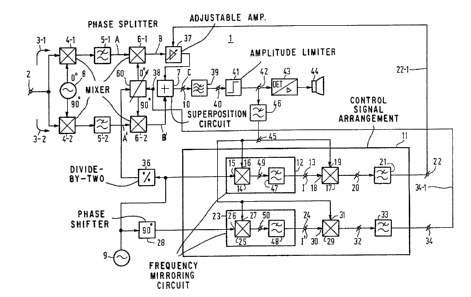
The receiver 1 shown in Figure 1, including two
35 quadrature signal paths 3-1 and 3-2 connected to an input
2 is used in integrated receivers for receiving, for example,
frequency~ amplitude or single-sideband modulated signals.
~Z~ 3
PHN.12235 6 15-9-1987
Each of the respective signal paths 3-1 and 3-2
includes a mixing stage 4-1 and 4-2, filter means indicated
in Figure 1 as a low-pass filter 5-1 and 5-2, and a mixing
stage 6_1 and 6-2, which are separately interconnected in
5 series in the respective signal paths 3-1 and 3-2. The
signal paths 3-1 and 3-2 are both connected to a superposit-
ion circuit 7. The mixing stages 4-1 and 4-2 are connected
to a generally tunable first oscillator 8~ whose quadrature
oscillator signals, represented by "0" and "90" are used
for a down-conversion of the received high-frequency signals
available at input 2. When tuning the oscillator frequency
within the frequency band of a received modu]ated high-
frequency signal~ a frequency folding around 0 ~z takes
place after mixing. The selection of a desired high-frequency
signal from the received signals is carried out in the low-
pass filters 5-1 and 5-2. The low-pass characteristics
of these filters 5-1 and 5-2 both show cross-over frequencies
having small values, generally realizing a steep descent
of the edges of these filters. The steep edges provide a
20 great selectivity and minimize the interference with the
signal selected by the filters 5-1 and 5-2 owing to adjacent
channels situated near the received high-frequency signal.
The receiver 1 includes a second oscillator 9
which applies the oscillator signal in quadrature to the
25 two mixing stages 6-1 and 6-2 through among other things
a phase splitter 60 in a manner to be disclosed hereinafter.
After the low-pass filtering, an up-conversion of the signals
in the parallel signal paths 3-1 and 3-2 is realized in the
mixing stages 6-1 and 6-2 to a generally fixed frequency
30 value of the oscillator 9. Generally, two folding sidebands
will occur, whose values will lie on both sides of the fixed
frequency value. The superposed circuit 7 has a signal output
10 at which an output signal is available which is realized
by superposing the output signals of the mixing stages 6-1
35 and 6-2, The superposition circuit 7 can be designed as
an adder or a subtractor depending on whether the band to be
demodulated is a low-frequency band or a high-frequency band.
If the frequency of the output signal of the oscillator 8
lZ99~9
PHN.12235 7 15-9-1987
is indicated by f1, that of oscillator 9 by fz and the
carrier frequency of the received high-frequency signal by
fc, the desired frequency band to be received is situated
around the frequency value f2-f1~-fc with the first version
5 of the superposition circuit 7, and around the frequency
value f2+f1-fc with the second version thereof. In the first
version the frequency band of a basically undesired error
component which will further be explained lies at approxi-
mately f2+f1-fc and in the second said version this is
lO aPProximately f2-f1*f .
As the received high-frequency signal on input 2
is generally modulated, a frequency band around the said
desired and undesired frequency components of the signals
has been discussed above~ For simplicity it will be assumed
15 hereinafter that the received high-frequency signal is un-
modulated and only the carrier component is received.
Then it is possible to deal with frequency components
instead of frequency bands.
Figure 2a shows the spectrums of the signals
20 referenced ~ and A' as a function of the frequency; infor-
mation with respect to the phase of the signals is not
given in this Figure and the following Figures. After
mixing the signals A and A' with the oscillator signal having
a frequency f2 of the oscillator 9, the spectrums of the
25 output signals of the mixing stages 6-1 and 6-2 will arise
as shown in Figure 2b. The output signal at the signal
output 10 then has substantially two frequency components
which are situated on both sides of the oscillator fre-
quency f2. Figure 2c shows the two frequency components
30 referenced G and E of the output signal marked C for the
case in which the superposition circuit 7 is designed as an
adder. The desired carrier component is referenced G. The
above error component, referenced E, forms a reliable mea-
sure for any mutual differences in the signal processing
35 in the parallel signal paths 3-1 and 3-2. These differences
are the result of undesired amplitude and phase differences
between the signals B and B' applied to the superposition
circuit 7, as a result of which the error component E occurs
~Z~924~
PHN.12235 8 15-9-1987
together with the desired frequency component G in the
output signal at signal output 10. The presence of this
error component E leads to the fact that in case the received
signal is modulated, annoying distortion and whistling will
5 occur in the signal obtained after the output signal C
has been demodulated.
The receiver 1 shown in ~igure 1 includes a control
signal arrangement 11 for generating generally two control
signals in a manner to be discussed hereinbelow.
lO The first control signal forms a measure for the undesired
amplitude differences occurring between the signals and
the two signal paths 3-1 and 3-2; accordingly~ the second
control signal forms a measure for the occurring undesired
phase differences. An embodiment of a circuit in which the
15 control signals are used for reducing these amplitude and
phase differences is known per se from the European Patent
~pplication No. 122 657 discussed in the introductory part.
A further possible embodiment of such a circuit is shown in
Figure 1, in which, for example, in the signal path 3-1
20 between the mixer stage 6-1 and the superposition circuit 7
an adjustable amplifier (reducer) 37 is connected to the
first control signal output 22 still to be discussed~ so as
to reduce the unwanted amplitude differences by affecting
the amplification of the first control signal. It will be
25 evident that the adjustable amplifier can be positioned
anywhere in the signal path 3-1 or 3-2. Further, in such a
circuit the phase splittar 60~ for example, contains a phase
control having a phase control input 38. The phase control
input 38 is connected to the second control signal output
30 34 which is to be discussed hereinafter, for affecting with
the second control signal the phase quadrature relationship
between the quadrature oscillator signals applied to the
mixing stages 6_1 and 6-2. Instead of the phase controllable
phase splitter 60 also a non-controllable phase splitter 60
35 can be used in combination with a phase shifter inserted
at an arbitrary position in the signal path 3-1 or 3-2
connected to output 34.
~ Z99~
PHN.12235 9 15-9-1987
The receiver discussed in the aforementioned
European Patent Application includes among other things a
series arrangement of a carrier selection circuit with an
additional phase-locked loop connected to the superposition
5 circuit designed as an adder. By means of the output signal
of the carrier selection circuit the loop is excited.
A disadvantage hereof is that the acquisition time~ by which
is to be understood the time the loop needs to lock on this
output signal after being excited for the first time, is
lO relatively large. This is caused by the fact that the band-
width of the phase-locked loop is narrow.
As will be evident hereinafter no additional phase-
locked loop whatsoever is used in the receiver 1 still to be
discussed Therefore~ the receiver 1 will not be subject to
lS the above disadvantages resulting from the use of the
additional loop.
Thereto, the control signal arrangement 11 of the
receiver 1 includes a circuit to be called hereinafter first
frequency mirroring circuit 12 having a first mirror-sym-
20 metrical signal output 13. The first frequency mirroringcircuit 12 comprises a first further mixing stage 14.
The first further mixing stage 14 has two mixing inputs 15
and 16 and a mixing output 49. The first mixing input 15
is connected to the oscillator 9 in a manner to be discussed
25 hereinafter. The second mixing input 16 is connected to the
signal output 10 of the superposition circuit 7 also in a
manner to be discussed hereinafter.
Mixing the output signal at the signal output 10
with the oscillator signal having a frequency value of twice
30 f2 of oscillator 9 causes the two frequency components
G and E to become available at the first mirror-symrnetrical
signal output 13 as mirror-symmetrical values of f2. The so-
called first frequency mirror-symmetrical signal available
at the first mirror-symmetrical signal output 13 is refe-
35 renced I. The two mirror-symmetrical frequency components
G and E are shown in Figure 2-d.
The control signal arrangement 11 comprises a
first mixing stage 17 of a third pair of mixing stages having
lZ9~
PHN.12235 10 15-9-1987
two mixing inputs 18 and 19 and an output 20. The first
mixing input 18 is connected to the first mirror-symmetrical
signal output 13 whilst the second mixing input 19 is coupled
to the signal output 10; in Figure 1 by being connected to
5 the second mixing input 16. The control signal arrangement
11 comprises a first low-pass filter 21 connected to the
output 20 and having a first control signal output 22.
As the respective components G and E in Figures 2c and 2d
are situated mirror symmetricallyt at a like frequency,
lO after mixing in the first mixing stage 17 of the third
pair a so-called first control signal with a DC current
eomponent will occur at output 20. The DC current component
of the first control signal occurring at first control sig-
nal output 22 after passing through the low-pass filter 21
15 is referenced K in Figure 2e. This first control signal in
the form of a DC current component forms a reliable measure
for the unwanted amplitude differences occurring between
the signals in the two signal paths 3-1 and 3-2. Through
the feedback circuit 22-1 of the controllable amplifier 37
20 this first control signal is supplied for correcting the
amplitude of the signal oecurring in the signal path 3-1.
The embodiment of receiver 1 shown in Figure 1
eomprises the control signal arrangement 11 as well as a
so-called second frequency mirroring eircuit 23 having a
25 second mirror-symmetrieal signal output 24. The seeond
frequency mirroring circuit 23 comprises a second further
mixing stage 25. The second further mixing stage 25 has two
mixing inputs 26 and 27 and a mixing output 50. The first
mixing input 26 is connected in a phase quadrature relation-
30 ship to the oscillator 9 through a 90 phase-shifting
network in a manner to be discussed hereinafter. The second
mixing input 27 is connected to the signal output 10 of the
superposition circuit 7 and is connected to the second
mixing input 16.
Mixing the output signal at the signal output 10
with the phase quadrature oscillator signal having a fre-
quency value f2 of the oscillator 9 causes the two frequency
eomponents G and E to be available at the second mirror_
g;~49
PHN.12235 11 15-9-1987
symmetrical signal output 24 as a mirror-symmetrical value
f f2. The so-called second frequency rnirroring circuit
available at the second mirror-symmetrical output 24 is
referenced I' and the frequency spectrum corresponds to the
5 spectrum represented in Eigure 2-d.
The control signal arrangement 11 further comprises
a second mixing stage 29 of the third pair of mixing stages
having two mixing inputs 30 and 31 and an output 32. The
first mixing input 30 is connected to a second mirror~
lO symmetrical signal output 2~, whilst the second mixing
input 31 is connected to the signal output 10; in Figure 1
by being connected to the second mixing input 16. The control
signal arrangement 11 comprises a second low-pass filter 33
connected to the output 32 and having a second control
lS signal output 34. After mixing in the second mixing stage 29
the second control signal having a DC current component will
arise at the output 32 in a manner already discussed for
the first control,signal. After low-pass filtering the DC
current component alos referenced by the letter K in Figure
20 2e is available at the second control signal output 34.
This second control signal in the form of the DC current
component forms a reliable measure for the undesired phase
differences occurring between the signals in the two signal
paths 3-1 and 3-2 and is applied to the phase control input
25 38 of the controllable phase splitter 60 through the feed-
back circuit 34-1 in order to correct the mutual phase of
the "0" and "90" phase quadrature oscillator signals.
The oscillator 9 is connected to the first mixing
input 15 and through among other thi~gs the 90 phase
30 shifter 2,8 having the first mixing input 26. Realizing a
frequency mirror symmetry around the oscillator frequency
f2 situated substantially equidistant from the two frequency
components G and E by means of the two frequency mirroring
circuits 12 and 23 is achieved in a simple manner by giving
35 the frequency of the signal at the first mixing input 15
and owing to the phase-shifting network 28 at the first
mixing input 26 a value of 2 x f2. The linking of the
respective mixing stage 6-1 in signal path 3-1 and the
g
PHN.12235 12 15-9-1987
mixing stage 6-2 in signal path 3~2 with the oscillator
9 can then be realized by means of a divide-by-two divider
36 to be implemented on a chip in a simple manner. The
divide-by-two divider 36 is inserted between the oscillator
5 9 and the phase splitter 60.
Between the oscillator 9 and the mixing stages
6-1 and 6-2 low-pass filters can be inserted, if so desired,
with a view to suppressing any disturbing higher harmonics
in the oscillator signal.
An advantageous feature is the fact that the
receiver 1 cancels phase and amplitude differences~ caused
by the mixing stages 4-1, 4-2 as well as the low-pass
filters 5-1, 5-2 and mixing stages 6-1, 6-2.
The explanation given so far is based on the outl~lt
15 signal at signal output 10 containing two frequency compo-
nents. This is correct, essentially. However, when taking
a closer look at the spectrum of the output signal at signal
output 10, referenced C, as shown in Figure 2c, it is shown
that so-called false frequency components also occur in the
20 signal. A plurality of these false frequency components
are shown in the Figures 2b and 2c referenced Si and S'
(for i = 1, 2 and 3). The component S1, for example, is
caused by the fact that a fraction of the input signal A
and A' ends up in the output signal ~ at signal output 10
25 through the mixing stages 6-1 and 6-2 and the supsrposition
circuit 7. The components S2 and S3 are the components
with two frequency components G and E mixed around the third
harmonic of f2.
The receiver shown in Figure 1 comprises a band-
30 pass filter 39 for allowing to pass, for example, bothcomponents G and E. It is advantageous that the bandpass
filter 39 is permitted to be such a wideband filter that
the two components are allowed to pass. If so desired~ it
is also possible to allow to pass only the desired carrier
35 component G, surrounded by the frequency band arisen during
the modulation of the received high-frequency signal.
The bandpass filter 39 has an output 40 to which
an amplitude limiter 41 having an output 42 can be connected.
~zg~z~
P~IN.12235 13 15-9-1987
It is advantageous that a detector known per se and an
amplifying circuit 43 with a loudspeaker 44 can be connected
straight to output 42. More specifically, when using the
receiver in mobile systems, in which the received signal
5 is generally provided with amplitude modulations due to
interference by multipath distortion, the signal at output
42 is free from these amplitude modulations which are
&nerally considered annoying. If desired, the output 42
can be connected straight to the mixing inputs 16, 19, 27
lO and 31.
The receiver 1 shown in Figure 1 includes a
lowpass filter 46 having an output 45 connected to the
output 42 and the mixing inputs 16, 19~ 27 and 31. In this
case the receiver 1 includes no more than one low-pass
l5 filter 46 used for disposing of spectral signal variations
at output 45, which have develGped, for example, during an
amplitude-limiting process. Thus~ the spectrum of the signal
at output 45 contains only the two frequency components
G and E.
The receiver 1 shown in Figure 1 further includes
a low-pass filter 47 connected between the mixing output
49 of thc first further mixing stage 14 and the first mirror-
symmetrical signal output 13, and a low-pass filter 48
connected between the mixing output 5O of the second further
25 mixing stage 25 and the second mirror-symmetrical signal
output 24. Using the low-pass filters 47 and 48 will cause
the spectral variations in the signals on the mirror-sym-
metrical signal outputs 13 and 24 developed during the
mixing process to be suppressed. Thus, the spectrum of the
30 signals on the outputs 13 and 24 only contains two mirror-
symmetrical frequency components E and G.
A further advantage of the receiver 1 explained
hereinbefore is the fact that the configuration of each
of the signal paths 3-1 and 3-2~ the structure of the first
35 further mixing stage 14 the low-pass filter 47 and the first
mixing stage 17, as well as the configuration of the second
further mixing stage 25, the low-pass filter 48 and the
second mixing stage 29 is always the same, that is to say,
~IZ~t9Z~9
PH~-.12235 14 15-9-1987
the configuration of a low-pass filter inserted between two
mixing stages. This equivalent configuration induces the
receiver 1 to be implemented on a chip in a simple manner.
For the oscillators 8 and 9 square-wave oscilla-
5 tors are to be preferred, producing a square-wave oscilla-
tor signal having opposite amplitude values during equal
periods of time. In practice, such a square-wave signal
contains a substantially negligeable DC current component
as a result of which amplitude and/or phase variations
lO due to D~ offsets in the signal paths 3-1 and 3-2 are
suppressed.