Note: Descriptions are shown in the official language in which they were submitted.
~299Z58
Contact Elements for Miniature Inductor
This invention relates to miniature induc-
tors and particularly to the ~ecuring of contact
element~ on the inductor so that the inductor can be
surface mounted to a printed circuitboard.
The inductor con~i~ts of a ferromagnetic
core, a winding around the core, and contact elements
to which the ends of the winding are soldered.l T~
inductor is surface mounted to the copper pattern~~ide
of a printed circuitboard. The inductors to which the
preaent invention is directed are tiny, having a
maximum dimension of about lilO inch.
U. S. Patent No. 4,588,974, assigned to the
aQsignee of the present invention, discloses a mount-
ing o~ contact element~ to an inductor core. In that
patent, the elements are shallow, U-shaped copper
strips who3e legs are cli~mped against the side3 of the
core to hold the copper to the core until ~he epoxy-
1- adhesive sets. The '974 patent has not provided the
best solution to the attachment problem. The attach-
ment has not been completely reliable becau~e the
epoxy doe~ not bond well to the copper, the copper
~299ZS8
-2-
having a thin film of copper oxide to which the epoxy
doe~ not bond well. Further, from an electr$cal
standpoint, the clo~e proximity of all of that copper
to the core and winding adversely affect the Q of the
inductor. The problem of attachment ari~es particu-
larly in the mass producing of tiny inductors wherein
the copper contacts having dimensions of about .020
inch by .070 inch are to be bonded to the core.
Because of the difficulty of adhering epoxy to copper,
that surface area ~imply i8 too small to make a good,
reliable bond. If the contact elements were made with
a larger bonding area to make a better attachment, too
much copper would be introduced and positioned too
close to the winding, with the result that the Q
degrades.
An objective of the present invention has
been to provide a mounting of a contact element to a
miniature inductor that provides a good bond ana
!significantly improves the Q of prior confiqurations.
This objective is attained by using conventional
printed~circuitboard material as a contact element.
The printed circuitboard material is a laminate of an
impregnated fabric such a~ fiberglAss forming a base
and copper with tin plating covering the exposcd
125 surface of the copper. The preferred material is
thin, being about 0.010 inch in thickness with the
base being about 0.007 inch thick and the copper being
~299258
-3-
rom .001 inch to .003 inch thick. The base could be
up to about .030 inch thick.
In the forming of sheet~ of printed circuit-
board material, it i9 pos~ible to apply processing
S techniques by which a very good adherence between the
ba~e material and the copper i~ attained--that i8, an
adherence that cannot be attained when one i8 attempt-
ing to ma3s produce tiny little contact ~trip~ mounted
to tiny core members. Epoxy is relatively ea~y to
adhere to another epoxy-base~ material such a~ fiber-
glass boArd. Thus, the use of printed circuitboard
material, which has an epoxy-impregnated ba~e, solve~
the adherence problem since the tiny contact elements
formed of that material can be bonded by the epoxy to
the core with relative ease. But there i~ an addi-
tional benefit arising out of the use of the printed
circuitboard material in that the 7 mil thick fiber-
glas act~ a~ a ~pacer of the copper away from the
winding on the core, thexeby improving the Q by a
factor of 5 - 10~.
The several features and objective~ of the
prasent invention will become more readily apparent
from the following detailed description taken in
con~unction with th~ accompanying dxawing~ in which:
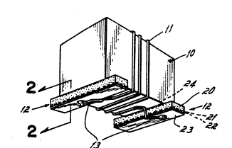
Fig. 1 i8 a perspective view of an inductor
and formed in accordance with the pre~ent invention~
; and
--3-- .
- . ~
~2 99;258
Fig. 2 is a cro s-sectional view taken along
lines 2-2 of Fig. 1.
Referring to Fig. 1, there is shown a core
around which a winding 11 i8 mounted. Contact
elements 12 are securad to the core. The windlng has
ends 13 that are soldered to the contact element~.
That inductor i~ uitable for surface mounting to the
copper pattern of a printed circuitboard by soldering
the contact elements to the copper on the printed
circuitboard.
The inductor is tiny. It has dim2nsions
which will be set forth below. The~e dimensions will
vary 30mewhat but are set forth here to provide the
order o~ magnitude of size o~ inductor to which the
present invention i8 applicable. The core i9 . 100 to
.250 inch long, .090 to .200 inch wide, and .050 to
.150 inch high. The spacing between the contact
elements 12 is about .060 inch. Each contact element
is about .020 inch wide and .070 inch to .200 inch
long.
As best shown in Fig. 2, the contact element
12 i8 formed from a laminate of an epoxy base fiber-
glass fabric 20 which is about .007 inch thick and
copper 21 that is between .001 inch and .003 inch
1 25 thick. The copper iq bonded to the fiberglas~ by an
adhesive 22 in accordance with the convention~l
practices in making printed circuitboard material.
~299Z~;8
-5-
The copper i8 usually clad wi~h a tin plate indicated
at 23.
~ach contact element 12 i9 attached to the
core 10 by means of an epoxy 24.
It can be seen from Fig. 2 that the .007
inch ba~e material spaces the copper strip 21 a sub-
stantial di3tance away from the core and the winding,
thereby improving the Q of the inductor.
From the above disclosure of the general
principle~ of the present invention and the preceding
deta$1ed description of a preferred embod$ment, tho~e
skilled in the art will readily comprehend the var$ous
modifications to which the pre~ent invention is
susceptible. Therefore, I desire to be limited only
by ~he scope of the following claims and equivalents
thereof:
-5-