Note: Descriptions are shown in the official language in which they were submitted.
~2~g~
~CKGROUND OF THE INVENTION
This invention relates to a method and apparatus
for switching an optical connector ancl, more
particularly, to a method and apparatus for momentarily
switching the op-tical connector.
Op-tical connectors are used when connecting optical
transmission units which mainly contain optical fibers
with reproducibility known per se.
Optical connector made of plastic or metal attached
integrally to the end of the optical trasmission unit is
generally employed as one of the optical connec-tors,
which has centering engaging holes at both sides.
When the optical transmission units are connected
to each other through such optical connec-tors, the front
end faces of paired optical connectors are opposed to
each other, and pins may be engaged with the engaging
holes coincident to each other in the opposed state.
In an optical communlcation, defects, alteration of
connection or tran~fer o~ existing or presently used ray
line (optical communicatlon cable) occur at a
considerable rate. Partial zone or entire ~one of the
existincJ ray line is replaced by a new optical line at
every time. Thus, the connecting works of the existing
ray line must be executed at every time.
In this case, the optical transmission units for
forming the ray line are separated at the connection
unit with -the abo~e-mentioned optical connectors, and
the optical -transmission units are again connec-ted
through the optical fibers.
When replacing the optical cable with the existing
ray line of the ac-tive line state composed of the
optical cables, it is re~uestsd to switch and connect
the optical transmission units without disturbance as
much as possible in the transmission of existing
information (optical signals) in case of replacing the
existing ray line of active line state composed of the
optical cables.
For example, in order to suppress the interrupting
time of an optical signal to 40 msec. or shorter of the
maximum allowable time, it is necessary to complete the
switching work with the optical connec-tors in an
extremely short time within the allowable time.
However, it is general to connect optical
transmission un:its through optical connectors or
separate the op-tical transmission units at the
connection units of the optical connectors depending
upon the worker's skill. Even skillEul worker -takes
sev0ral tens seconds ordinarily when disassembliny the
optical connectors of the connected state and then
reconnecting the disassembled one optlcal connector with
~Lr~ n~
an optical connector prepared separatPly, and
information (optical signals) is interrupted in the
existing ray line during the period.
The switching of the optical connectors is
discussed to he mechanized or automated so as to shorten
the replacing wvrk, but desirable method and apparatus
for replacing the optical transmission units are not yet
provided at present.
SUMMARY OF THE INVENTION
Accordingly, an object of this invention is to
provide a method and an apparatus for switching an
optical caonnector which can eliminate the
abovementioned drawbacks and can momentarily switch to
connect optical transmission units with optical
connectors without depending upon a worker's skill as
well as mechanize or automate the replacing work.
In order to achieve the above and other objects,
there is provided according to the present Lnvention a
method for switching an optical connector having paired
optical connectors opposed at front end faces thereof,
pins engaged with engaging holes penetrating linearly
longitudinally at the optical connectors to connect both
the optical connectors to each other in such a manner
that one of both the optical connectors of connected
state is for recornnecting ~nd the other is for
separating so that the reconnecting optical connector is
connected to the switching optical connector having an
engaging hole prepared separately comprising connector
disposing step of disposing the switching optical
connec-tor in parallel with the separating optical
connector, pin forward moving step of moving the pins
engaged with both the reconnecting and reparating
optical connec-tors each other to the reconnecting
optical connector side by means of a pushing rod
inserted from the rear end face of the separating
optical connector into the engaging hole to remove the
pins from the separa-ting optical connector, to be
executed in an arbitrary sequence, then connecting
switching step of relatively moving the reconnec-ting
optical connector, the separating optical connector and
the switching optical connector along the front end
faces thereof to separate the separating optical
connector from the reconnecting optical connector and
simultaneously bringing the front end face of the
reconnecting optical connec-tor and the front end face of
the switching optical connector in coincidence with each
other, and then pin backward moving step of moving the
pins of the reconnecting optical connector side to the
switching optical connector side by means of a pushing
rod disposed at the rear end face side of the
19~
reconnecting optical connector to engage the pins with
-the engaging holes of the swi~.ching optical connector to
dispose the pins over the reconnecting optical connector
and the separating optical connectorO
According to another aspect of the present
invention, there is also provided an apparatus for
switching an optical connector having paired optical
connectors opposed at front end faces thereof, pins
engaged with engaging holes pene-trating linearly
longitudinally a-t the optical connectors to connect both
the optical connectors to each other in such a manner
that one of both the optical connectors of connected
state is for reconnecting and the other is for
separating so that reconnecting optical connector is
connected to the switching optical connected having an
engaging hole prepared separately comprising a main base
for holding the reconnecting optical connector, a
subbase for holding the separating optical connector and
the switchi.ng optical connector in parallel, the main
and subbases being disposed relatively movably in such a
manner that the front end faces thereof are opposed to
each other, the pin pushing rods engaged within the
engaging holes of the optical connectors and pushing rod
operating means provided on the main and subbases,
whereby at least one of the main and subbases has moving
means for relatively moving the main or subbase in a
desired direction.
In case of the method for switching -the optical
connector of the invention, the optical connectors are
replaced momentarily by less and simple steps without
waste in the work, such as connector disposing s-tep, pin
forward moving step, connector switching step and pin
backward moving step. Thus, optical signal interrupting
time can be extremely shortened in the replacemen-t of
the optical connector in the existing ray line of the
active line state.
In case of the apparatus for switching the optical
connector of the invention, since the apparatus
comprises the main base for holding the reconnecting
optical connector, the subbase for holding the
separating optical connector and the switching optical
connector, the pin pushing rods engaged in the engaging
holes of the optical connectors, pushing rod opera-ting
means and moving means for moving the main base and the
subbase relatively in a desired direction, the steps of
the above-mentioned optical connector switching method
can be mechanically automated to establish the
automation oE the method for switching the optical
connector.
The above and other related ob~ects and fea-tures of
the invention w.ill be apparent Erom a reading of the
following descriptiorl of the disclosure found in -the
accompanying drawings and the novel-ty thereof pointed
out in the appended claims.
BRIEF DESCRIPTION OF THE DRAWINGS
Fig. 1 is a perspective view of an optical
connector handled in a method and apparatus for
switching the optical connector according to the present
invention;
Fig. 2(a) through 2 (e) are explanatory views
sequentially showing the steps of a first embodiment of
a method for switching an optical connector according to
the present invention;
Figs. 3(a) through 3(d) are explanatory views
showing the steps of an essential portion of a second
embodiment of a method for switching an optical
connector according to the invention;
E~igs. ~, 5 and 6 are views showing the steps of an
essential portion of other embodiments of a method for
switching an optical connector according to the
invention;
E'ig. 7 is a characteristic diagram showing the loss
of an example of switching an optical connector
according to the invention;
E'ig. 8 is an explanatory view schematically showing
4C~
embodiments except the above embodimen-ts of a me-thod for
switching an optical connector of the invention;
Fig. 9 is a plan view showing an embodiment of an
apparatus for switching an op-tical connector according
to the present invention; and
Fig. 10 is a front view of the apparatus.
DESCRIPTION OF THE PREFER~ED EMBODIMENTS
Embodiments of a method and an apparatus for
switching an optical connector according to the present
invention will be described in detail with reference to
the accompanying drawings.
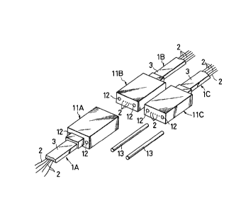
In Fig. 1, mul-ticore coated optical transmission
units lA, lB, lC each having a flat rectangular
sectional shape are each ~ormed of a plurality of
optical fibers 2 integrally coated through a coating
layer 3.
The coated optical transmission units lA, lB, lC
each becomes the conskituent unit of an optical cable
unit, which, in turn, becomes a constituent unit of an
optical cable, which i8 used as a ray line.
In Fig. 1, optical connectors llA, llB, llC are
formed of plastic or metal, and each formed at both
sides with engaging holes 12 which penetrate
longitudinally the optical connector.
Such optical connectors llA, llB, llC are
1;2~3~
respectively integrally attached to the ends of the
coated optical transmission units l~, lB, lC, and the
optical fibers 2 are exposed at the end faces in the
same plane as the front end ~aces of tl-e optical fibers
2 a~ the front end faces of the optical connectors ll
llB, llC.
The above-mentioned op-tical connectors llA, llB,
llC might also be attached to the ends of a plurali-ty of
single core coa-ted optical transmission units aligned in
parallel with each other.
In Fig. 1, pins 13 are members for connecting
either two oE the above-mentioned optical connectors
llA, llB, llC.
Each such pin 13 has an outer diameter relatively
engaged precisely with the engaging hole 12 of each of
optical connectors llA, llB, llC and a length over the
engaging holes 12 of both op-tical fiber~ opposed to each
other.
Figs. 2(a) through 2(e) se~uentially show the steps
of an embodimen-t of a method for swltching an optical
connector according to this invention.
In case of Fig. 2(a), paired optical connectors llA
and llB a.re opposed at the front end faces, the pins 13
are engaged into two engaging holes 12 coincident in the
opposed state to connect both the optical connectors 11
and llB -to each othe.r.
One llA of both the optical connectors llA, llB of
the above-mentioned connecting state is for
reconnecting, and the other llB is for separating, and
the optical connector llA for reconnecting is switched
to be connec-ted with a switching optical connector llC
prepared separately.
Thus, as shown in Fig. 2(a), the switching optical
connector llC is disposed in parallel with -the
corresponding optical connector llB at the side of the
optical connector llB for separating.
In Fig. 2(a), when a pin pushing rod 47 disposed at
the side of the rear end face of the separating optical
connector llB is initially moved forward toward -the
optical connector llB, the pin pushing rod 47 enters the
engaging hole 12 of the separating optical connector llB
as shown in Fig. ~(b) to move the pin 13 to the
reconnecting optical connector llA side and to remove
the pin 13 from the separating optical connector llB.
Then, as shown in Fig. 2(c), when the reconnecting
optical connector llA is moved i.n a predetermined
distance to the switching opt.lcal connector llC side
along the end :Eace thereof~ the reconnect.ing optical
connector llA and the separating opti.cal connector llB
are separated from each other, and the front ends oE the
~Lf~ 8
reconnecting optical connector llA and the switching
optical connector llC simultaneously coincide with each
other.
The pin pushing rod 47 moves backward in -this
meantime -to re-turn to the original position.
Thereafter, as shown in Fig. 2(d), pin pushing rods
40 disposed at the side of the rear end face of the
reconnecting optical connector llA is moved forward
toward the op-tical connec-tor llA, and the pin pushing
rods 47 thus moved forward are contacted with the pins
13 disposed at the side of the reconnecting optical
connector llA.
After the contacting, the pins 13 are moved through
the pin pushing rods 40 to the switching optical
connector llC ~ide to be engaged with the engaging holes
12 of the switching optical connector llC, and the pins
13 are thus disposed over between the reconnecting
optical connector llA and the separati~g optical
connector llC/ thereb~ completing the switching of the
optical connectors.
Thereafter, as shown in Fig. 2(cl), the pin pushing
rods 40 are moved backward to be returned to the
original positions.
The method of this ivention i~ based on the above-
mentioned operations according to predetermined steps.
~;~9~ 8
However, the method of -this invention may addi-tionally
employ other embodiments described below.
One o~ the other embodimen-~s precedes the step of
moving forward the pin in the relative relation to the
steps of disposing the connec-tors ~in Fig. 2(a)) and the
step o~ moving forward the pins, and follows the s-tep of
disposing the connectors.
~ owever, as in the sequence disclosed in Figs. 2,
it is preferable in the execution without interrup-ting a
series of works -to move forward the pins 13 after
disposing the separating op-tical connector llC at the
predetermined position.
Another oi the other embodiments relatively moves
one of the reconnecting optical connector llA, -the
separating optical connector ll~ and the switching
optical connector llC at a small dis-tance in a direction
for separatLng the front end faces thereof as shown in
Fig. 3(a) before starting the step of switching and
moving the connectors in Figs. 2(b) and 2(c) to set a
fine gap ~1 between the front end faces o both the
connectors.
Such fine gap L1 i8 ordinarilly set to 10 to 30
of the stroke oE the pin 13.
In this case, in movlng the connectors in the later
time, there is no possibility that the front end faces
13
of the separating optical connector llB and the
switching optical connector llC are damaged by the ends
of the pins 13 engaged only with the engaging holes 12
of -the reconnecting op-tical connector llA.
After -the fine gap L1 of Fig. 3 (a) is set, the
connecting switching work is carried out in the se~uence
of Figs. 3((b), 3(c) and 3(d) and 3(d). In Figs. 3(c)
to (d), both the optical connectors llA and llC are
relatively moved in a predetermined direction so as to
oppose the front end faces of the reconnecting optical
connector llA and the switching optical connector llC so
as to eliminate the fine gap L1.
In this operation, when the reconnecti.ng optical
connector llA is fixed and the separating optical
connector llB is moved in a predetermined direc-tion, the
switching optical connector llC is ordinarily moved
together with the separating optical connector llB.
Yet another one of the other exbodiments, before
the pins 12 are removed ~rom the separating optical
connector llB in the pin forward moving step in Figs.
2(a) to 2~b), the pins 13 are temporarily stopped as
shown in Fig. 4, and the pina 13 are again moved
therea~ter to remove the pins 12 :~rom the separating
optical connector llB.
The reason is as will be described.
14
It is necessary to switch the optical connectors in
a-t least two connection units when partial zone of the
ray line is replaced with new ray line in the existing
ray line.
In this case, assume tha-t one optical connector is
initially switched and -the other optical connector is
then switched, a signal interrupting time at the
existing ray line is lengthened, but when these two
op-tical connectors are simultaneously switched, the
signal interrupting time is reduced by half.
Further, when the signal transmitting state is held
as long as possible in the simultaneous switch;ng of the
optical connectors, and the optical connectors oE the
connecting units are simultaneously switched, thereby
shortening the signal interrupting time.
The state shown in Fig. 4 described above maintains
that part of the pins 13 is engaged within the
separating optical connec-tor llB even if the switching
work of the optical connectors is advanced to the
midway. Thu~, the optical connecting state i~ still
maintained by both the optical connectors llA, llB at
the existing ray llne.
In the Eollowing pin forward moving step, part of
the pins 13 remaining in the engaging holes 12 of the
separating optical connector llB is removed to suppress
~9~
the irregularity of removin~ t}le pins 13 to the minimum
limit.
Therefore, the switching works of the connection
units are simultaneously executed from the state in Fig.
4 to shorten the above-mentioned signal interrupting
time.
Still another one of the o-ther embodimen-ts executes
the following connector switching step while remaining
the pushing rods 47 inserted into the engaging holes 12
of the separating optical connector llB as shown in Fig.
5 in the pin moving step of Figs. 2(a) to 2(b), and
carries out the connector switching step.
More specifically, when moving to next connector
switching step after the pushing rods 47 are removed
from the engaging holes 12 of the separating optical
connector llB, the start of the next step is delayed in
the time of removing the pushing rods 47, but, as shown
in Fig. 5, when the next step is star-ted while remaining
the pushiny rods 47 in the engaging holes 12 oE the
separating optical connector llB, the switching work is
rapidly completed that much.
The embodiment in Fig. 5 may be applied to the case
of Fig. 3.
The last one of the othe.r embodiments temporarilly
stops the movement of -the pins as shown in Fig. 6 at the
o~
midway of engaging part of the pins 12 of -the
reconnecting optical connector llA si~e within -the
engaging holes 12 of the switching op-tical connector llC
in the pin backward moving step of Fig. 2(d), measures
the connecting loss by the reconnecting optical
connector llA and the switching optical connector llC
during the stopping time, continues the pin backward
moving step when the connecting loss is smaller than the
allowable value, and recovers the connection with the
reconnecting optical connector llA and the separa-ting
optical connector 12B when the connecting loss exceeds
the allowable value.
The reason for this is to advance khe completion of
the recovering work when the connecting loss after the
optical connector is switched is large.
In other words, the transmission loss
characteristic of the optical connector switching
example when employing the embodiment in Fig. 6 is as
shown in Fig. 7.
In Fig. 7, Pl and P2 designate startinq and
finishing points when the front halve~ of the pins 13
are removed fxom the engaging holes 12 oE the separating
optical connector llB in the pin forward movLng step, P2
and P3 de~ignate starting and finishing times when the
rear halve~ of the pins 13 are removed simllarly from
17
the engaging holes 12 of the separating optical
connector llB, -tl designates consuming time of P2 to P3,
t2 designates consuming time of the connector switching
step, P4 and P5 designate s-tarting and finishing times
when engaging the rear halves of ~he pins 13 in the
engaging holes 12 of the switching optical connector
llC, -t3 designates consuming times of P4 to Ps, to
designates temporary stopping time of the pins 13 in the
pin backward moving step, P6 and P7 designa-te starting
and finishing times when the rear halves of the pins 13
are removed from the engaging holes 12 of the switching
optical connector llC in the pin removing step in the
recovering work, t4 designates consuming time of P6 to
P7, P8 and Pg designate starting and finishing times of
backwardly moving the reconnecting optical connector llA
in the recovery work, ts designates consuming time of P8
to Pg, Pg and P1o designate starting and Einishing time
when engaging the rear halves of -the pins 13 wLth the
engaging holes 12 of the separating optical connector
llB in the recovery work, t6 designatés consuming time
of R8 to Pg, Plo and Pll designate starting and
finishing times when engaging the rear halves of the
pins 13 with the engaging holes 12 of the separating
optical connector llB, TS designates the interrup-ting
time Oe the optical signal, and l'R designates a recovery
18
~y~
working time.
The connecting loss of the reconnecting optical
connector llA and the switching optical connector llC is
measured at the temporary stopping time to in the above
operation, and when the connecting loss is lower than
the allowable value, the pin backward moving step is
continued, while when the connecting loss exceeds the
allowable value, the connection oE the reconnecting
optical connector llA and the separating op-tical
connector llC is recovered.
In the embodiments described above, predetermined
switching work can be executed by fixing arbitrary one
of -the reconnecting optical connector llA, the
separating optical connector llB and the switching
optical connector llC in the relative relation and
moving the other. Thus, the reconnecting optical
connector llA may be fixed and the separating optical
connector llB and the switching optical connector llC
may be moved contrary to khe above operation.
The movin~ operations of the pin~ 13 will be
naturally var:Led iTI respect of th:Ls.
In the embodiments described above, the switching
optical connector llC has been disposed at -the side of
the separating optical connector llB when swi-tching the
optical connector. ~lowever, such switching optical
lg
connector llC may be disposed under (above~ the
separating optical connector llB as shown in Fig. 8. In
this case, the above-mentioned operati.ons are all
effective.
Further, when switching the optical connec-tor
attached to the single-core op-tical transmission unit,
the above-mentioned method is also effective.
Figs. 9 and 10 show an embodiment of an apparatus
for switching an optical connector according to this
invention.
The apparatus of this invention in Figs. 9 and 10
is disposed ordinarily in the connectiny portions at
both ends of a zone to be switched of the ray line to be
used to switch the optical connector of the connnecting
portions.
In Figs. 9 and 10, a base 30 has a rectangular flat
shape, the upper surface of the base 30 has high and low
steps in such a manner that one side upper surface
becomes a low surface 30a and the other aide upper
surface becotnes a high surface 30b.
A pair of guide rails 31a disposed in parallel are
laid along Yl-Y2 direction in Fig. 9 on the low surface
30a of the base 30, sliders 31b are slidably engaged
with the guide rails, 31a, a movable base 32 is
installed over the slider6 31b so that the base 32 is
movable in Y1~Y2 direc-tion.
The level o~ the base 32 is the same as the high
surface 30b of -the base 3n.
A block 32a having a threaded hole in -the axial
cen-ter is fixed along the Y1-Y~ direction at the center
on the lower surface of the base 32.
A drive shaft 33 is engaged with the threaded hole
of the block 32a, and the drive shaft 33 i5 connected to
the output shaft of a drive motor (stepping motor)
through a coupling 33a.
Thus, the base 32 moves in the Y1-Y2 direc-tion by
normal or reverse rotation of the drive motor 34.
Guide rails 35a are laid along Xl-X2 direction oE
Fig. 9 on the upper surface of -the base 32, sliders 35b
are slidably engaged with the guide rails 35a, a main
base 38 is attached to -the sliders 35b so that the base
38 is movable in the X1-X2 direction.
A block piece 36a having a threaded hole of Xl-X2
direction is fixed to the axial center at the center on
the lower surface of the rear end (X1 ~ide of Fig. 9) of
the base 36.
A drive shaft 37 :is engaged with the threaded hole
of the block piece 36a, and the drive shaEt 37 i9
connected through a coupling 37a to the output shaft of
a drive motor (stepping motor) 38.
l~hus, the base 36 moves in the Xl-X2 direction ~y
the normal or reverse rotation oE the drive motor 38 on
the base 32.
An L-shaped holder 36b is formed at the upper
surface of the front end o~ the base 38 (at the side of
X2 in Fig. 9)l and formed in size adapted wi~h the
optical connector llA.
The vertical wall 38c which forms part of the
holder 36b of the base 38 is perforated with two through
holes 36d disposed in parallel longitudinally through
the vertical wall 38c, and a groove 38e for engaging
coated optical -transmission unit lA is formed on the
upper surface of the vertical wall 38c.
~ he through holes 36d correspond to the pin pushing
rods 40 described with respect to the above-men-tioned
method to be rela-tively engaged with each other.
A pair of pin pushing rods 40 inserted from the
rear end face side of the vertical wall 36c are attached
wi-th holders 40a at the base ends -thereof.
A groove 40b is formed on the upper surface of the
holder 40a for engaging the coated optical transmission
unit lA.
A drive shat 41 having a threaded hole parallel to
the pin pushing rod 40 i.s engaged with the center on the
lower end of the holder 40a, and connected through a
coupling 41a to the output shaft of a drive motor
(stepping motor) 42, which is disposed at khe rear end
side on the base 38.
Thus, the pin pushing rod 40 is telescopically
forward or backward in the X1-X2 direction in the
through hole 38d and the engaging hole 12 of -the optical
connector llA by the normal or reverse rotaion of the
drive motor 42.
Guide rails 43a are laid along X3-X4 in Fig. 9 on
the high surface 30b of the base 30, sliders 43b are
slidably engaged Wit}l the guide rails 43a, a subbase 44
is fixed to the sliders 43b, and is movable in -the X3-X~
direction.
A bJ.ock piece 44a having a threaded hole in the X3-
X4 direction in the axial center is ~ixed to the center
on the lower surface of the rear end (at the X4 side of
Fig. 9) on the subbase 44.
A drive shaft 45 is engaged wi-th the threaded hole
of the block piece 44a, and connected through a coupling
45a to the output shaft of a drive motor (stepping
motor).
The sub base 44 is moved forward or backward
in the X3-X4 dlrection by the normal or reverse rotation
of a drive mokor 43.
An inverted ~-shaped holder 44b is formed on the
~9~
upper surface at the front end of the subbase 44 (at the
side o~ X6 in Fig. 9), and is formed in size adap-ted to
the optical connectors llB, llC aligned in parallel.
Two parallel through holes 44d pene-tra-ting
longi-tudinally through the ver-tical wall 44c for formin~
part of the holder 44b are opened at the subbase 44, and
grooves 44a, 44f are formed on the upper surface of the
vertical wall 44c for engagirlg the coated optical
transmission units lB, lC.
The through holes 44d correspond relatively to the
pin pushing rods 47 described with respect to the method
of the ivention, and are aligned linearly with the
through holes 36d.
A pair of pin pushing rods 47 inserted ~rom the
rear end face sides of the vertical wall 44c into the
through holes 44d are attached at the base ends thereof
with holders 47a.
A drive shaft 48 having a threaded hole parallel to
the pin pushing rods 47 is engaged with the center on
the lower end of the holder 47a, connnected -through a
coupling 48a to the output shaEt of a drive motor
(stepping motor) 49, which i8 mounted at the rear end
8ide on the subbase 44.
rrhus, the pin pushing rods 47 ar telescopically
movable forward or backward in the Xl-X2 direckion in
24
the th.rough hole 44d and the pin engaging holes 12 of
the optical connector llB.
~ position detecting sensor 50 is mounted on the
subbase 44 to move together with the subbase 44, and the
position detecting sensor 50 detects the moving position
of the pin pushing rods 47.
More specifically, the position detecting sensor 50
is connected -to the input side of a controller, not
shown, and when the pin pushing rods 47 move forward to
a predetermined position, a predetermined signal is
supplied to the controller.
The drive motors 34, 42, 46, 49 are electrically
connected to the output side of the controller, which
outputs a drive signal to the drive motors.
When the above-mentioned method is executed by the
switching apparatus shown in Figs. 9 and 10, the
reconnecting optical connector llA and the separating
optical connector llB connectèd to each o-ther are set
over the holder 38b of the main base 36 and the holder
44b of the subbase 44, and the switching optical
connector llC i8 set in parallel with the separatlng
optical connector llB.
Then, the pin pushing rod~ 40, 47 and the main base
36 and the subbase 44 for holding the reconnecting
optical connector llA, the separating optical connector
~;29~
llB and the switching optical connec-tor llC are moved at
suitable predeternlined distance in the ~l-Y2 direc-tions
through predetermined drive
system and guide means to swi~ch the optical connectors
described with respect to Figs. 2 to 6.
In this case, the controller for holding the
position detecting sensor 50 suitably controls the
movement and the stop of the pin pushing rods 40, 47,
the main base 38 and the subbase 44.
In ~he switching apparatus in Figs. 9 and 10, when
the optical connectors are switched as shown in Fig. 8,
a combination construction o~ the pin pushing rods 40,
47, the main base 38 and the subbase 44 are
correspondingly altered in design, and the moving means
and the guiding means are similarly altered in design.
In the switching apparatus in Figs. 9 and 10,
arbitrary actuator is employed as means for moving the
pin pushing rods 40, 47, and a machanism utilizing a
spring or a solenoid may be, for example, employed in
addîtion to the drive motor (stepping motor) as shown.
~ urther, the method and the apparatus o~ this
invention may switch the optical connectors in one zone
or a plurality oE zones a-t existing ray line.
According to the method oE this invention, the
optical connectors are replaced momentarily by less and
26
~z~
simple steps wi-thout waste in the work, such as
connector disposing step, pin forward moving step,
connector switching step and pin backward moving step
without depending upon the wor]cer's skill. Thus,
optical signal interrupting time by the switching can be
extremely shortened.
~ ccording to the apparatus of this invention, the
main base, the sub base, the operating means of the pin
pushing rods, relatively moving means of the main base,
and the subbase are functionally associated. Thus, the
steps of the above-men-tioned op-tical connnector
switching method can be mechanically automated to
establish the automation of the method for switching the
optical connector.