Note: Descriptions are shown in the official language in which they were submitted.
12~
PARALLEL OPERATING SYSTEM FOR ALTERNATE
CURRENT OUTPUT CONVERTERS
BACKGROUND OF TH~ INVENTION
Field of the Invention
The present invention relates to a means used in a power
supply system for parallel operation of a plurality of
alternate current output converters, such as inverters,
connected with a common load, for controlling balance of
currents between converters.
Prior art systems will be discussed in detail
hereinbelow.
SUMMARY OF THE INVENTION
An object of the present invention is to provide a
parallel operating system in which, even if a breakdown is
caused on a converter of a plurality of converters in parallel
operation, no adverse effect due to an excessive cross-current
will be produced on other sound converters in parallel
operation.
Another object of the present invention is to provide a
parallel operating system achieving high speed controlling of
the load current shared among a plurality of converters in
parallel operation and further capable of controlling
instantaneous allotment of the current.
A further object of the present invention is to provide a
parallel operating system capable of preventing the
interference between the effective current and the reactive
current thereby improving the response speed of control.
`- ~Z~6~
Yet another obj ect of the present invention is to provide
a parallel operating system whereby it is made possible to
make even the ratios of the load current shared amony a
pl~rality of converters in parallel operation, with the
capacity of each converter taken into account.
A still further object of the present invention is to
provide a parallel operating system not only applicable to
parallel operation of inverters but also generally applicable
to parallel operation of other converters of an
instantaneously controlled type.
The parallel operating system for A.C. output converters
according to the present invention is not of an average value
control but of a high frequency PWM inverter of an
instantaneous value control, and moreover, it is structured
based on inverters of an instantaneous current value control
type provided with a current minor loop for controlling the
instantaneous value of the output current. The current minor
loop is adapted to be supplied with a command value from a
voltage major loop and a command value obtained from the load
current which corresponds to the share of the load current to
be borne by each converter, as the command value for the
current to be output by the converter for maintaining the
output voltage at a sine-wave.
The parallel operating system for A.C. output converters
of the present invention while maintaining a sine-wave bus
voltage by means of its current minor loop controlling the
instantaneous value of the output current of the converter,
provides, as the command value to the minor loop, the command
v
val~e from the voltage major loop and the command value
corresponding to the share o* the load current to be borne by
each converter, thereby restraining occurrence of the cross-
current in the event of a breakdown caused on another
converter.
In accordance with one aspect of the invention there is
provided in a parallel converter system for operating a
plurality of sine-wave converters in parallel, each thereof
including a filter, with outputs thereof connected to a common
bus and a share of a load current allotted to each, said
parallel operating system for alternate current converters
comprising, for each converter: converter body executing
conversion of an instantaneous current control type by means
o~ an arm of each phase constituting the converter body
performing a plurality of switching op~rations during one
cycle time to thereby control an instantaneous value of an
output current; means for establishing a sine-wave output
voltage reference synchronized with a load bus voltage; means
for determining a share of a load current to be borne by each
converter based on a detected value of the load current and
providing a first signal corresponding to said determined
value; and voltage control means for detecting an error
between the load bus voltage and said sine-wave output voltage
reference and providing a second signal for correcting said
error, wherein a sum of said first signal and second signal is
provided as a current command value for said converter.
The above and other objects and features of novelty of
the invention will become more fully apparent from the
following detailed description taken in conjunction with the
accompanying drawings, which are solely for illustration and
description and not for limiting the scope of the present
invention.
BRIEF DESCRIPTION OF THE DRAWINGS
FIG. 1 is a block diagram showing a prior art paral].el
operating system for A.C. output converters;
FIG. 2 and FIG. 3 are block diagrams showing a parallel
operating system for A.C. output converters according to an
embodiment of the present invention;
FIGs. ~(a) and ~b) and FIG. 7 are circuit diagrams
showing an embodiment of a converter for use in a system of
the presPnt invention;
FIG~ 5 is a circuit diagram for detecting a load current
to be allotted in the parallel operating system of FIG. 2;
FIG. 6 is a circuit diagram for more precise control of
the current to be allotted in FIG. 5:
FIG. 7 is a circuit diagram showing a high-frequency
inverter according to another embodiment o~ the present
invention; and
FIG. 8 is a diagram for explaining a high-frequency link
converter.
DETAILED DE5CRIPTION OF THE PREFE~RED EMBODIMENTS
FIG. ~ is a diagram showing a prior art parallel
operating system for A.C. output converters as disclosed, for
example, in Japanese Patent Publications No. 53-36137 and
56-1310.
Referring to the diagram, a first inverter 1 is operated
,~
6~
in parallel with a second inverter 2 of the same structure
connected through an output bus 3 for supplying power to
load 4. The first inverter 1 is structured chiefly o~ an
inverter body 100, a reactor for filter 102, and a capacitor
for filter 103, and connected with the output bus 3 through an
output switch 104, and it is adapted to convert power from a
D.C. power source 5 into A.C. power~ In order to achieve the
parallel operation of the inverters 1 and 2, a detected signal
I1a is first obtained by a CT 106 from the output current I1 of
the first inverter 1. Then, the difference between a detected
signal I2a similarly obtained from the second inverter 2 and
the detected signal I1a, namely, a signal a I corresponding to
the cross-current is obtained by a cross-current detector
means 107. Thereupon, two voltage vectors EA and EB crossing
each other at right angles are formed by a phase shifter 108,
and these and the signal ~ I are operated upon in arithmetic
circuits 109 and 110 and a reactive power component ~ Q and an
effective power component ~ P are obtained from these,
respectively. The inverter performs a pulse width modulation
(PWM) for the inverter body 100 by means of a voltage control
circuit 113 and a pulse width modulation circuit 114 based on
output signals from a voltage setting circuit 111 and a
voltage feedback circuit 112 and thereby controls the internal
produced voltage.
~5 Meanwhile, the reactive power component ~ Q is supplied
to the voltage control circuit 113 as an auxiliary signal, so
to speak. The voltage control circuit 113, in response
thereto, adjusts the internal produced voltage of the inverter
~29~5~
body 100 several % thereby reducing the reactive power
component ~Q to zero.
On the other hand, the effective power component ~P is
supplied through an ampli~ier 115 forming a PLL circuit to a
reference oscillator 105 to finely adjust its frequency, and
hence, the amplifier 115 and the reference oscillator 105
function so as to control the phase of the internal produced
voltage of the inverter body 100 thereby reducing the
component ~P to zero.
Thus, by controlling the voltage and phase to reduce ~ Q
and ~ P to zero, the cross-current between two inverters are
eliminated and stabilized sharing of the load between them is
attained.
However, there have been problems with the above
lS described prior art system as follows. A first problem is
that, when one of the inverters in parallel operation is
broken down and thereby the voltage on the broken inverter
becomes extremely low, or high, it is possible that an
excessive cross-current flows through another sound inverter
~0 and thereby this sound inverter also breaks down.
A second problem is that, since average values of the
phase and the voltage of the internal produced voltage of the
inverter is controlled to control the current for the load
shared between the inverters and the allotted share of the
~5 current is thus controlled indirectly, it is dif~icult to
improve the responding speed or accuracy of the controlling
operation, and especially, it is impossible to control
instantaneous allotment of the current.
1~2996~0
A third problem is that the control of the effective
current and that of the reactive current are not per~o~med
independently but they interfere with each other, and to avoid
this interference, the response speed of the control cannot be
raised so much.
A fourth problem is that, when the reactance values of
the reactors of the filters of the three-phases are not equal
but different from each other, the ratios of the allotted
currents becomes different between phases.
The prior art parallel operating system for converters
has been structured as described above and involved those
problems as mentioned above, of which, it has been a primary
problem that, when a breakdown occurs on one of the inverters
in parallel operation and thereby the voltage on the broken
inverter becomes extremely low, or high, an excessive cross-
current flows through another sound inverter and thereby this
sound inverter also gets out of order.
An embodiment of the present invention will be described
below with reference to the accompanying drawings.
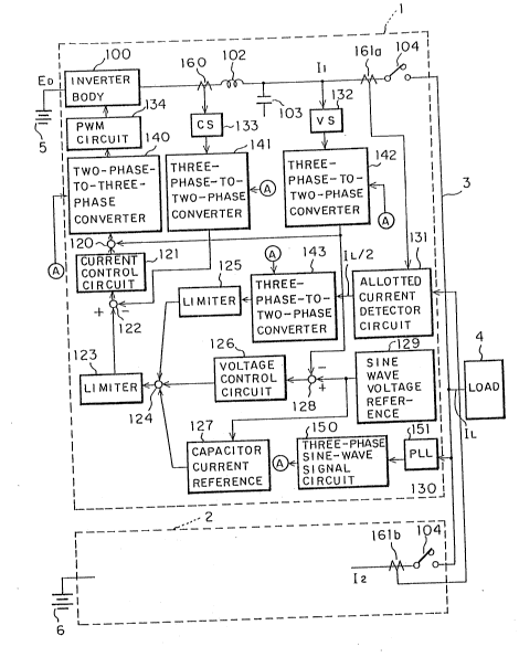
FIG. 2 is a block diagram showing a parallel operating
s~stem for A.C. output converters according to an embodiment
of the present invention. Referring to the figure, a first
inverter 1 is in parallel operation with a second inverter 2
of the same structure, not shown, through an output bus 3 for
supplying power to a load 4. Parts in FIG. 2 corresponding to
those in FIG. 1 are denoted by corresponding re~erence
numerals. However, while FIG. 1 is showing an inverter o~ the
type controlling the average value of the output voltage,
. ~
~.
--` 129~6~j~
FIG. 2 shows an inverter of the type controlling
instantaneous values of the output current and voltaye,
and hence, the circui~s are not always of the same
function.
The inverter body 100 is ~ormed, for example, of
transistors or power MOSFE~s capable of high-frequency
switching, and allows each arm of a three-phase bridge
inverter as shown in FIG, 4(a) or a single-phase bridge
inverter as shown in FIG. 4 (b) to switch at a high
requency as high as 10 times to several hundred times
the output frequency (e.g., 60 Hz). While the timing of
the switching is determined by PWM circuit, this PWM
circuit, for example, is a sine wave/triangular wave
comparison PWM circuit performing the switching at each
intersection of a triangular carrier wave and an output
voltage command signal.
~he present inverter provides a current minor loop,
and therein, a current control circuit 121 delivers a
control signal to a PWM circuit 134 so that the output
current fed back through a CT 160 and a current sensor
133 may coincide wlth a current command from a limiter
123. Since there are voltages of counter-electromotive
force from a capacitor 103 and the other, second, inver-
ter 2 on the output bus, the inverter body 100, in order
to control the output current, is required to produce
the sum of the voltages of counter-electromotive force
and the voltage to be applied to a reactor 102. Hence,
-- 8 --
, :
650
the output bus voltage is detected by a voltaye sensor
VS 132 and added to the output of the current control
circuit 121. By so doing, the current control circuit
121 is only required to control the voltage applied to
the reactor 102, and thereby, its controlling performance
is enhanced. Meanwhile, a PLL 130 produces a sine wave
voltage reference 129 in synchronism with the voltage on
the output bus 3. A capacitor current reference 127
produces a reference sine wave current leading the
voltage reference by 90 as the current to flow through
the capacitor 103, corresponding to the capacitance of
the capacitor 103. An allotted current detector circuit
131 derives, from the current in the first inverter
detected by a CT 161a and the current in the second
inverter detected by CT 161b, the instantaneous value of
the current to be borne by each inverter, IL/n, e.g.,
the load current IL divided by the number n of inverters
in parallel (n = 2 in the present case).
If the converters are of different capacity, hence
2~0 the current to be allotted is not l/n of the load
current, a current value corresponding to different
ratio of allotted currents is derived according to the
capacity of the inverters.
A voltage control circuit 126 produces a correction
current signal for the inverter to correct the
discrepancy between the output voltage and the sine
wave voltage reerence 129.
6~C~
Now, operations will be described. First, in the
no-load state, the inverter supplies the current to flow
through the capacitor 103 and thereby a no-load voltaye
is established. At this time, the voltage control
circuit 126 corrects for the voltage error occurring due
to the error in the current control or the discrepancy
between the actual current value through the capacitor
103 and the capacitor current reference 127.
At this time, the output voltages of the two
inverters are both controlled by their PLL 130 to be put
in phase with the output bus 3 and they are put in
parallel operation.
Upon turning on of the load 4, a command is issued
from the allotted current detector circuit 131 to the
current minor loop to bear 1/2 of the load current IL
whereby each inverter bares a 1/2 share of the load
current IL. Here, a limiter 125 limits the overcurrent
such as a rush current so as not to continue upon the
turning on of the load and a limiter 123 is to limit the
final current command value to below the allowable value
for the inverter.
By arranging the parallel operating system as
described above, the inverter is protected from an
overcurrent by means of its own current minor loop and
enabled to maintain the output voltage at a sine wave by
quickly responding to distortions or sudden changes in
the load current. What is characteristic of this system
-- 10 --
3 Z~g~5~1
is that the control as described above is perforlaed at
each switching ~iming in the high-frequency PWM and
therefore very quick response is attained. When a
switching frequency at 10 KHz is used, for example, the
control is performed every 100 ~s, and therefore, a
transient phenomenon due to an external disturbance such
as a sudden change in the load can be completed within
about 10 times of 100 ~s, whereby excellent controlling
performance can be obtained.
Although it is a well known art, a concrete example
of the allotted current detection will be described
below with reference to FIG. 5. Let us consider the
case where a load current of 300 A are borne as Il =
90 A, I2 = 100 A, and I3 = 110 A by three inverters,
INV-l, INV-2, and INV-3, respectively, and there are
produced voltages of 9 V, 10 V, and 11 V respectively
across the burden resistors Rll, R21, and R31 for the
CT-l, CT-2, and CT-3. Across each of resistors R12,
R22, and R32 which are sufficiently larger than the
resistors Rll, etc., there is developed (9 + 10 + 11)/3
= 10 V This voltage corresponds to 1/3 of the load
current and the current value to be borne by each
inverter, and hence, this signal being insulated can be
introduced into the control circuit. In the foregoing
description, it was neglected that the currents are
vector quantities for simplicity's sake, but the same
relationship holds if they are dealt as vector
quantities.
-- 11 --
: . -
6~
When, the INV-l, for example, is to be ~topped,
first a switch S12 is shorted, whereupon the voltaye on
the resistors R22 and R32 each becomes 15 V and the load
comes to be borne wholly by the other two inverters.
Then, a switch S12 is turned on and simultaneously the
output switch for the inverter is opened so that it is
released from the parallel connection.
In the circuit of FIG. 5, for example across the
resistor Rll, there is obtained a signal corresponding
to the current being borne by the INV-l, and across the
resistor R12, there is obtained a signal corresponding
to the current to be borne by the INV-l. Further,
between the point Xl and the point X2, there is obtained
a voltage corresponding to the discrepancy ~I of the
current borne by the INV-l. Hence, by additionally
providing a circuit, as shown in FIG. 6, for insulating
and amplifying the signal ~I between the points Xl and
X2 and supplying the signal to an adder 135 in FIG. 2,
the discrepancy of the borne current can be reduced
further. It is apparent, when the gain in the circuit
of FIG. 6 is raised further, that the balanced allotment
of the load will be attained even if the circuit to
supply the allotted current command from the allotted
current detector circuit 131 in a feeding-forward manner
in FIG. 2 is omitted. This idea can also be implemented
for the embodiment of FIG. 3.
- 12 -
.
``" ~.2~
The above described control system of FIG. 2 is
applicable to both single-phase inverters an~ three-phase
inverters, and, not only applicable to inverters, it is
widely applicable to other instantaneously controllable
converters such as cycloconverters as well.
A system using a synchronous rotating coordinate
system with d - q axes, which provides more excellent
characteristics in operating three-phase inverters or
converters, will be described below with reference to
FIG. 3.
The configuration in FIG. 3 is virtually the same
as that in FIG. 2 but greatly differs therefrom in that
it has three three-phase-to-two-phase converters 141,
142, 143 and one two-phase-to-three-phase converter 140.
A three-phase sine-wave signal circuit 150 and a PLL 151
synchronizing the circuit with the output bus voltage
produce the following six signals as three-phase sine-
wave signals as the references for the pertinent
coordinate transformation.
SU = ~ sin (~t + ~)
SV = ~ sin (~t - 2~/3 + ~) ..... (1)
SW = ~ sin (~t + 2~/3 + ~)
CU = ~ cos (~t + ~) 1
CV = ~ cos (~t - 2~/3 + ~) ~ ....... (2)
Cw = ~ cos (~t + 2~/3 + ~) J
(where ~ is usually set to ~ = 0).
- 13 -
~Z~:3~1~5(~
When three-phase s.ignals of the current sensor 133,
the allotted curren-t detec-tor circuit 131, and the
voltage sensor 132 are represented by the expression
X = col[Xu, xv, Xw], by multiplying the following
transformation matrix C to the same, these are converted
into the D.C. signals Y = col[Yd, Yq~ alony d - q axes
as follows.
C = [Su SV SWl ................................ (3)
CU CV W
~Y ~ ~CU V W Ixwl
where ~ above character indicates a matrix and ^
indicates vector quantities along d - q axes. Upon such
transformation, if the .inverter output voltage commands
are expressed as
sin ~t
V * = ~E sin (~t - 2~/3)1 .................... (5)
sin (~t ~ 2~/3)
their values along the d - q axes are given by
V * = ~ cd ~ = C V * = ~ (6)
cq
Further, when the capacitance of the capacitor 103 is
denoted by Cp, the current commands Ic* for the currents
to be passed therethrough will be expressed as
- 14 -
3650
~I d*~
c lV * J = C Ic* = C ~ Cp Ecq
cos ~t 0
cos (~t - 2~/3) = ..... (7)
cos (~t + 2~/3) ~ ~ Cp É
Thus, a three-phase sine-wave signal becomes a D.C.
constant along d - q axes. As against the control of
S the three-phase system of U-, V-, and W-phases of FIG. 2
in which errors are liable to be produced even in the
normal state because of it being a variable value
control system, control essentially producing smaller
errors can be attained in the present control system
being a constant value control system.
When the ordinary sine-wave triangular-wave
comparison system is to be used for the PWM moduIation,
signals therefor of the three-phase, U-, V-, and W-phase,
system become necessary. Hence, the following inverse
transformation matrix (8) is multiplied to the control
signals to thereby return them to the three-phase system
again and the signals~are supplied to the PWM circuit.
SU CU
C~l SV ~Cv .................................... (8)
: SW C
In the above described embodiments based on FIG. 2
and FIG. 3, the controlling capability is designed to
- 15 -
~9~0
be improved by supplying, as the command value for the
current minor loop, the curren-t value to be passed
through the parallel capacitor in the inverter output
filter, but the capacitor current reference 121 in
FIG. 2 and FIG, 3 may be omitted. This is because the
voltage control circuit 126 functions so that the output
voltage may coincide with the sine-wave voltage
reference 129, and as a result, it produces a signal
substituting for the signal of the capacitor current
reference 127, thereby smoothly functioning as a control
system for the sine-wave inverter. In such a case, a
sufficiently large amplification factor of the voltage
control circuit 126 reduces the discrepancy in the
voltage control.
Although, in the above description, the case where
the present invention was used for parallel operation of
inverters was explained, the same principle can be
applied to other instantaneously controllable current
converters, such as a high-frequency link converter as
shown in FIG. 7 comprised of a combination of high-
requency inverters and cycloconverters, in which D.C.
power is converted to a high-frequency rectangular wave
and further to a low-frequency sine wave.
In the converters shown in FIG. 7, a rectangular
wave as shown in FIG, 8(a) is obtained by switching of
transistors Ql to Q4 at the secondary side of the
transformer TR. Then, a sawtooth wave synchronized with
_ 16 -
o
switching of the inverter as shown in FIG. 8(b) is
produced, and in-tersections of the same with -the ou-tput
voltage command signal as indicated by the line Xl - X2
in the figure are obtained as shown in FIG. 3(c). Then,
by selecting switches of the cycloconverter as indicated
in FIG. 8(e) depending on the polarity of this signal
and the voltage RS of the inverter, the voltage
corresponding to the signal Xl - X2 as shown in
FIG. 8(d) is obtained between N and P in FIG. 7.
As apparent from the above explanation, the circuit
of FIG. 7 is that which is able to obtain a single phase
PWM voltage equivalent to that from FIG. 4(b). Further,
in the case of providing three-phase output, such a
three-phase high-frequency link converter as uses three
sets of the secondary side of the transformer TR of
FIG. 7 may be used. The principle shown in FIG. 2 and
FIG, 3 may be implemented by a discrete circuit
including an analog operational amplifier, etc., or by a
software treatment by digital control using a micro-
processor or a digital signal processor.
Although explanation was given above with twoinverters of the same capacity used for the sake of
brevity, the invention can also be applied to parallel
operation of n converters of different capacities. In
such a case, each of the converters will be e~abled to
bear its share of the load in proportion to its capacity
by arranging such that the CT-l, CT-2, CT-3, etc. and
- 17 -
6S0
11~ R21, R31, e-tc. are chanyed according
to the capacities and -the same voltages appear at the
terminals across Rll' R21' R31~ etc- when the rate~
current flows.
Although two limiters 123 and 125 are used in the
embodiments of FIG. 2 and FIG. 3, the limiter 125 may be
omitted only leaving the limiter 123, or, even if neither
of the limiters 123 and 125 is used, the saturation limit
of the amplifier may be used for the limiter.
As understood from the above description, the
present paxallel operating system has the following
features. First, the output current of the converter is
restricted by the command value issued to the current
minor loop, and therefore, even if the output of another
converter suddenly changes due to its breakdown or the
like, there i5 no possibility of a breakdown of the
sound converter due to a cross current passing through
this sound converter. Secondly, since the instantaneous
value of the output current of the converter is directly
controlled in the present system, a quick .response to
the allotted current and precise control of it is
possible. Provided that the switching frequency of the
converter is sufficiently high, excellent control of
allotted current can be performed, even duriny a
: transient phenomenon, because the allotted current can
be instantaneously controlled in the interval of the
switching period. Thirdly, in the case of three-phase
- 18 -
~LZ~96~)
operations, a control system can be set up along d - q
axes to thereby obtain a non-interactive control system
capable of quick-response control along both the d axis
and the q axis. Fourthly, since the value LS of the
output filter is included in the current minor loop,
even if the values are not equal among three phases the
discrepancy can be compensated for.
The present invention having many eatures as
mentioned above is adapted to obtain a sine-wave voltage
while performing parallel operation of converters with a
current minor loop controlling the instantaneous value
of the output current, and therefore it produces the
effect to restrict overcurrents such as a rush current
from the load or a cross current due to a voltage change
in another converter due to its sudden breakage. Thus,
a highly reliable system can be structured.
- 19 -
:
. .