Note: Descriptions are shown in the official language in which they were submitted.
~2g~
BACKGROUND OF THE INV~:NTION
This inven-tion relates -to a method oE diree-t
memory access control for a system eomprislng input/
ou-tput deviees, memory and control processor, such as an
electronic switehing system, in whieh the input/output
devices send direct memory aeeess requests to the
proeessor.
The direet memory aeeess eontrol between
input/output deviees and a proeessor is deseribed, for
example, in artiele entitled "Architecture of a Distri-
buted Packet Switehing System", in publication "Switching
Research", SE84-121, pp. 37-42. In this packet switching
system, -the line unit as an input/output deviee has a
function of direct memory aecess. The line unit (input/
output deviee), when making direct memory aeeess, sends
a proeessor bus holcling request signal to the proeessor.
Upon reeeiving the request signal, the proeessor holds
the proeessor bus whieh eonnee-ts the line units to the
processor regardless oE time needed to have a transmission
Of direct memory aecess inEormation (memory address
ancl data) between the line unit and proeessor, and
thereafter grants the line unit a direet memory access
to the memory.
In this ease, if the transmission of direet
memory aeeess information between the line unit and
d~
~a2~
1 processor takes a long time, the processor holds the
processor bus long -time at the execution of direc-t
memory access, and therefore the processor cannot
access to the memory in this pexiod, resultiny in a
lower processing speed of the processor.
SUM~L~RY OF THE INVENTION
An object of this invention, which is intended
for a sys-tem comprising input/output devices, memory and
a control processor, is to reduce the processor bus
holding time at direct memory access by an input/output
device, thereby improving the processing speed of the
processor.
Another object of this invention is to provide
a method of direct memory access by holding the processor
bus for a constant time length regardless of time needed
for the transmission of direct memory access information
between input/output devices and processor.
In order to achieve the above objectives, the
inventive method employs a first and second buffer
registers and associated control means located between
the input/output devices and processor. Direct memory
access in~ormation (memory address and data) ~rom an
input/output device is stored temporarily in the second
buffer register, and then sent to the processor so that
it holds the processor bus to grant the direct memory
access. An input/output command from the processor to
an input/output device is stored temporarily in the first
~29~
1 buffer register, and then sent to the input/output
device so that it is executed. The bufEer register
control means issues a direct memory access request
signal to the processor after the second buffer regis-ter
has received all direct memory access information from
the input/output device, and the processor responds to
the request signal to hold the processor bus. Conse-
quently, direct memory access is carried out merely by
holding the processor bus for a constant time length.
BRIEF DESCRIPTION OF THE DRAWINGS
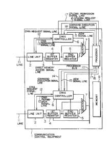
Fig. 1 is a block diagram of the communication
control equipment based on this invention;
Fig. 2 is a flowchart showing the operation of
the communication equipment 1 in Fig. 1;
Fig. 3 is a timing chart showing, as an example,
the memory write operation in direct memory access mode
by the line unit 6 in the communication control equip-
ment l;
Fig. 4 is a timing chart showing, as an example,
the execution by the processor 8 of the input/output
command to the line unit 6;
Fig. 5 is a timing chart showing, as an
example, the case of bus contention between the direct
memory access and input/output command shown in Figs.
2 and 3;
Fig. 6 is a schematic diagram of the DMA
control circuit 6 in Fig. 1;
~2~
1 Fig. 7 is a schematic diagram of the bus
arbitration con~rol circuit 601 in Fig. 6; and
Fig. 8 is a schematic diagram of the sequence
control circuit in Fig. 6.
5 DESCRIPTION OF ~HE PREFERRED EMBODIMENTS
An embodiment of this invention will now be
described with reference to Figs. 1 through 8. In Fig.
1, indicated by 1 is a communication control equipment
based on this invention and 2 is a line unit which is
an input/output device of the communication control
equipment and is designed to implement the direct memory
access control using LSI devices, etc. in compliance
to the CCITT-recommended X.25 protocol. Indicated by
3 is a direct memory access signal line used to transfer
memory address and data between the line unit 2 and
processor 8 in direct memory access mode, 4 is a first
buffer register according to this invention, 5 is a
second buffer register according to this invention, 6 is
a DMA controller which controls the first and second
buffer registers and also controls the direct memory
access operation, 7 is a selector for switching the
buffer registers 4 and 5, 8 is a procesor, 9 is a
memory, 10 is a procesor bus/ 11 is a line which connects
the terminal equipment to the communication control
equipment 1, 12 is a DMA request signal line used to
indicate a direct memory access request from the line
unit to the DMA controller 6, 13 is a DMA permission
~2~
l signal line used to indicate -the permission and comple-
tion of direct memory access from the DMA control.ler
6 to the line unit 2, 14 is a command execution signal
line used to indicate the execution of input/output
command by the processor 8 to the DMA controller 6, 15
is an ASW signal line used to indicate the reception
and completion of input/output command from the DMA
controller 6 to the processor 8, 16 is a CPUDMA request
signal line from the DMA controller 6 to the processor
8, and 17 is a CPUDMA admission signal line indicating
the reception of a CPUDMA request from the processor
8 to the DMA controller 6.
The following describes the operation of the
communication control equipment l on the flowchart of
Fig- 2- Communication data sent over the line 11 is
received by the line unit 2 in the communication
controller equipment 1. After processing the received
data, the line unit 2 sends a direct memory access
request to the DMA controller 6 over the DMA request
line 12 so as to store the d~ta in the memory 9: (step
116). The DMA controller 6, if the first and second
buffer registers 4 and 5 are empty and unless an input/
output execution command has been issued by the processor
8, sends a signal to the line unit 2 over the DMA
permission signal line 13 to indicate the permission of
direct memory access: (step 118). The line unit 2
sends the memory address and data (in case of memory
writing), which is direct memory access information,
.-- 5
~2~
1 to the first bufer register 4 over -the direct memory
access signal line 3: (step 120).
The DM~ controller 6, upon setting the address
and data in the first buffer register 4, transfers the
contents to the second buffer register 5: (s~ep 122),
and issues a direct memory access request to the
processor 8 over the CPUDMA request signal line 16:
(step 124). The DMA controller 6, upon receiving the
direct memory access permission signal from the processor
8 over the CPUD~ permission signal line 17: (step 128),
places the memory address and data from the second buffer
register 5 on the processor bus 10 by way of the
selector 7: (step 130). On completion of access to the
memory 9: (step 132), the DMA controller 6 disables the
signal on the DMA permission signal line 13, and indicates
the end of direct memory access to the line unit 2 to
complete the operation: (step 136). Fig. 3 shows an
example of the sequence of memory writing operation in
direct access mode. The memory reading operation .in
direct access mode is similar to the above memory writing
operation, and the explanation is omitted.
In the case of executing an input/output
command issued by the processor 8 to the line unit 2,
the processor 8 places the input/output command on the
processor bus 10, and then indicates the execution of
the input/output command to the DMA controller 6 over
the command execution line 14: (step 102). The DMA
controller 6 sends a signal over the ASW line 15
~2~97~
1 to indicate the reception of input/output command
execution to the processor 8: (step 106), and, after
setting the input/output command on the processor bus
10 in the first buffer register 4: (step 104), transfers
the input/output command to the line unit 2: (step 108).
Upon receiving the input/output co~nand, the line unit 2
executes it and, in case of the input command, returns
acknowledge information to the first buffer register
4. The DMA controller 6, when the acknowledge informa-
tion has been set in the first buffer register 4, placesthe contents on the processor bus 10 by way of the
selector 7: (step 110), and indicates the end of execu-
tion of input/output command to the processor 8 by
invalidating the signal on the ASW line 15: (step 112).
Fig. 3 shows an example of the sequence of the above
input command execution.
In case the direct memory access operation
taken by the line unit 2 and the input/output command
execution taken by the processor 8 contend with each
other: (step 126), the DMA controller 6 receives the
address and data in the first buffer register 4:
(step 120) and, after transferring the contents
to the second buffer register 5: (step 122),
sends the input/output command from the processor 8
to the line unit 2 using the first buffer reyister 4:
(steps 104-108), and sends acknowledge information, if
it is present, to the processor 8 by way of the first
buffer register 4: (step 110). After the input/output
~2~7~
1 command is completed, the DMA contxoller 6 proceeds with
the direct memory access opexation using -the address
and data held in the second buffer register 5: (steps
114, 128, 130~. Fig. 4 shows an example of the sequence
at the occurrence of contention between the memory
writing operation in direct memory access mode and the
input command execution.
As described above, the DMA controller 6
implements the direct memory access control, input/output
command execution control, and their arbitration
control.
Fig. 6 shows a more detailed arrangement of
the DMA controller 6. In the figure, indicated by 601 is
a 2-input arbitration control circuit, 602 is a sequence
circuit for producing the timing signals, 603 is a flip-
flop of set-reset type, 604 is an AND gate, and 605 is
an OR gate. Figs. 7 and 8 show the more detailed
arrangement of the arbitration control circuit 601 and
sequence circuit 602, respectively. The circuit shown
in Fig. 6 is to carry out the operation of Fig. 2,
although the explanation is omitted. The clocks I and
II used in Figs~ 7 and 8 have a 50% duty cycle and are
out of phase with each other by 180. It should be
noted that the circuit arrangements shown in Figs. 6, 7
and 8 are merely examples for realizing the DMA control
circuit 6.
According to this embodiment when the trans-
mission of direct memory access information between the
~2~g~2
l line unit 2 and processor 8 has an increased delay time
due to an increased length of signal line 3 or due to
the serial transmission on the basis of multiplex
memory address and data for reducing the number of
interface lines, the processor bus 10 at direct memory
access has a constant holding time, instead of being
affected by the transmission delay, whereby the process-
ing speed of the processor 8 is virtually prevented from
falling.
Although in the above description direct
memory access information is set in the second buffer
register by way of the first buffer registex, it is also
possible to practice the method by setting the informa-
tion directly in the second buffer register.
According to this invention, as described
above, when the transmission of direct memory access
information between the input/output device and processor
has an increased delay time due to an increased distance
between them or due to the serial transmission on the
basis of multiplex address and data lines for reducing
the number of interface lines for economy, the processor
bus at direct memory access can have a shorter holding
time, whereby the processing speed of the processor is
prevented from falling.
_ g