Note: Descriptions are shown in the official language in which they were submitted.
7219
,.
` lZ9~933
METHOD AND APPARATUS FOR APPLYING
ULTRA-THIN COATI NGS TO A SUBSTRATE
BACKGROUND OF THE INVENTION
The present invention relates to a method and
apparatus for applying a layer of coating material to a
substrate and, more particularly, to a method and appa-
ratus for applying a thin, virtually constant thicknesscoating to a substrate.
In many coating applications, extremely thin,
constant thickness coatings are absolutely essential in
order to avoid degrading the performance of the coated
device and/or the equipment with which such coatings
are utilized. In, for example, audio and video magnetic
tapes, if the magnetic media coating is excessively thick
or there are significant variations in coating thickness,
magnetic coupling and therefore information transferal
between the magnetic media in the coating and, for
example, a read/write head of audio or video recording
or reproducing equipment in which the tape is utilized
could be substantially degraded because of the increased
spacing or the spacing variations between these com-
ponents that necessarily result when such coatings areemployed.
A number of coating techniques presently exist
for applying coating materials to a web or other object
surface. Many of these techniques employ an electro-
static field between the coating applicator and the webor object surface to assist in both the uniform and
efficient deposition of coating materials on such
surfaces. In, for example, the well-known process of
electrostatic spray painting, an electrostatic field is
--1--
. .
129~933
established between an electrically conductive grid and
a particular metal object to be painted. The electro-
static field is created by a relatively high dc voltage
(100,000 V) connected between grid and object, with the
object ordinarily being spaced several feet from the
grid. Air pressure supplied to a reservoir of coating
fluid coupled to one or more orifices in the coating
applicator causes coating fluid droplet formation at the
output of each of said coating applicator orifices. The
droplets are subsequently propelled into the grid by air
pressure generated forces where they become electrostat-
ically charged and then deposited, in layer form, on a
surface of said particular object by forces associated
with the electrostatic field. Unfortunately, due to the
relatively large droplet size generated by this type of
coatiny apparatus, the resulting coating layers are well
in excess of a thickness level that would avoid the
above-mentioned problem associated with excessively
thick magnetic media coatings.
Electrostatic coating apparatus capable of
generating and subsequently depositing relatively small
coating material particles on a substrate has been
described in the patent literature. In U.S. Patent No.
2,685,536 to W. A. STARKEY ET AL, for example, a method
and apparatus for electrostatically coating articles are
disclosed wherein coating material is supplied to the
orifice of a coating applicator and an electrostatic
field is established between the surface of the coating
material and a surface of the article to be coated. As
described therein, the coating material oozes through
applicator orifices where it is then divided into fine
particles by forces associated with the electrostatic
field. The finely divided particles are then transported
to the surface of the article by forces associated with
the same electrostatic field.
1299g33
It can be demonstrated that the rate of elec-
trostatic field generated, coating material particle
movement toward a surface to be coated in, for example,
the above-noted STARKEY ET AL apparatus, is dependent,
in part, upon the intensity of the electrostatic field.
Therefore, variations in electrostatic field intensity
when coating, for example, a moving web will produce
corresponding variations in the thickness of an electro-
statically deposited coating layer. It is well known
that the intensity of an electrostatic field established
between a pair of electrodes spaced a fixed distance from
one another is very much dependent upon the shape of the
electrode ends between which the electric field is estab-
lished. The smaller the radius of curvature at the end
of an electrode, for example, the greater will be the
electrostatic field intensity in the vicinity of the
small radius of curvature electrode for any particular
electrode-to-electrode voltage. Variations in electrode
shape, therefore, can produce corresponding variations in
an electrostatic field in the vicinity of the electrode
surface where the shape is varying.
If, for example, the external surface of
coating material oozing through an applicator opening
in Fig. 2 of STARKEY ET AL, is considered to be an end of
an electrically conductive electrostatic field generating
electrode, variations in the shape of this external coat-
ing material will produce variation in an electrostatic
field in the vicinity of said coating material surface
and corresponding variations in the thickness of coating
material being atomized and deposited on a surface by
such a varying electrostatic field. Such surface shape
variations can be caused by any number of different
factors. One factor is the pressure variations that
are necessarily produced when a mechanical pump is is
employed to pressurize coating material supplied to the
--3--
- 1299~33
coating applicator. Another factor could be the presence
of air bubbles entrained within the coating material.
These bubbles would momentarily disturb or change the
external surface shape of the coating material when
passing through an applicator orifice. Yet another
factor might be changes in the coating surface shape
that may result as coating material particles are
electrostatically extracted from said coating surface
during the coating process. Each of these electrostatic
field intensity altering factors can produce variations
in web coating layer thickness.
Also, the electrostatic coating apparatus
described in STARKEY ET AL is employed where the object
to be coated is itself electrically conductive. In such
an arrangement, the ability to coat a particular object
is primarily dependent upon the ability to establish an
electrostatic field of sufficient intensity between the
coating applicator and a surface of the object to be
coated to both atomize the coating material particles
and then transport same to said object surface. However,
this type of coating apparatus is relatively ineffective
when employed to coat insulative materials, such as a
dielectric web, because the electrostatic field needed
to coat such materials is significantly attenuated by
the dielectric web. Present practice is to overcome
this problem by coating the web with an electrode forming
layer of electrically conductive material and then elec-
trostatically coat this layer with the preferred or final
layer of coating material. Unfortunately, this technique
both increases the cost of coating a web and adds the
characteristics of the conductive layer to that of the
coated web which may prevent its subsequent use in many
coated web applications.
In addition, it can readily be demonstrated
that fluids are dried by or have`moisture removed from
1299933
them when exposed to an electrostatic field. If coating
material flow rates are in the near-zero flow rate range,
as in the STARKEY ET AL patent, the external surface of
the coating material at the coating applicator orifices
or outputs may dry out or coagulate due to the presence
of an electrostatic field at said coating material
surfaces and thereby block or substantially reduce
the flow of coating material through each coating
applicator orifice, within a relatively short period
of time. A flow rate change of this type would also
produce detrimental variations in web coating layer
thickness.
It is a primary object of the present
invention, therefore, to provide coating apparatus
that is capable of applying a relatively thin, virtually
constant thickness layer of coating material to a
substrate.
It is another object of the present invention
to provide extremely low flow rate coating apparatus
having a flow rate that will remain fairly constant for
an extended period of time.
It is a further object of the present invention
to provide low flow rate coating apparatus that is
capable of properly functioning within an electrostatic
field for an extended period of time.
An advantage of the present invention is the
ability of the coating apparatus employed therein to
apply coating materials having significantly greater
conductivity than that of coating materials presently
applied by conventional electrostatic coating techniques.
Other objects, features and advantages of
the present invention will be readily apparent from the
following detailed description of a preferred embodiment
thereof taken in conjunction with the accompanying
drawings.
..
.
lZ99933
SUMM~RY OF THE INVENTION
In accordance with the present invention, a
low flow rate coating method and apparatus are disclosed
that are capable of depositing relatively thin, virtually
constant thickness coatings on a substrate. The method
and apparatus include a coating applicator coupled to a
source of coating material having an opening therein
formed of a dielectric material through which coating
material flows for substrate coating purposes. Means
are provided for forming a substantially unvarying shape
on the surface of that portion of the coating material
at said applicator opening, during the entire coating
process. The substrate is supported in a spaced relation
from the output of the coating applicator to thereby form
a coating gap between the coating applicator output and
said substrate. Means are provided for establishing an
electrostatic field in said coating gap between said
coating material surface and the substrate spaced
therefrom to thereby atomize or extract coating material
particles from said~ coating material surface and subse-
quently transport said particles to the substrate. Means
are also provided for moving the substrate at a constant
rate through said coating gap whereby a relatively thin,
uniform thickness layer of coating material is deposited
on said substrate. In dielectric web coating applica-
tions where a relatively thick layer of coating material
is required, an electrostatic charge is established on
the dielectric web at a location remote from the coating
applicator, before being moved past the coating appli-
cator opening, in order to neutralize electrostaticcharges present in the initial portion of the coating
layer that would otherwise interfere with (repel~ a
subsequently deposited portion of the same layer
necessarily having the same charge polarity.
-6-
:
:
...,
,
- 1299933
63356-1685
Accordlng to another aspect of the present lnvention,
there ls provided an extrusion-type coatlng appllcator for
applylng an extremely thin layer of coatlng material to a
substrate, said applicator havlng an lnput and an output and at
least said output is formed of dielectric material.
: , .... ....
1299933
BRIEF DESCRIPTION OF THE DRAWINGS
Fig. 1 is a diagrammatic illustration af a
web coating arrangement employing a preferred embodiment
of the coating method and apparatus of the present
invention.
Fig. 2A is primarily a side elevational view
of an enlarged detail of the dielectric output end of
the coating applicator nozzle shown in drawing Fig. 1.
Fig. 2B iS the same view as that in Fig. 2A
additionally showing changes in the shape of the coating
material surface at the applicator output that might
occur due to entrained gas bubbles and/or changes in
coating material pressure levels.
Fig. 3 shows a portion of the web coating
arrangement of drawing Fig. 1 and means for electro-
statically charging a dielectric web prior to depositing
coating material on a web surface.
DESCRIPTION OF THE PREFERRED EMBODIMENTS
The coating apparatus of the present invention
is capable of coating conductive as well as insulative or
high dielectric substrates. Presently available electro-
static coating apparatus such as that described in U.S.
Patent No. 2 ,893,894 to RANSBURG can readily coat con-
ductive substrates with relatively thick coatings, but
are relatively ineffective in coating dielectric sub-
strates. Inasmuch as the more difficult task is that of
coating dielectric substrates, the coating apparatus to
be described below is primarily directed to apparatus for
coating such substrates. However, this apparatus may be
employed to coat conductive substrates, also.
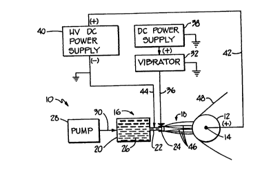
Turning now to Fig. 1 of the drawings, there
is shown a diagrammatic illustration of web coating
apparatus 10 employing the relatively thin, virtually
constant thickness coating method and apparatus of the
present invention. As shown in said Fig. 1, coating
i2999~
apparatus 10 includes cylindrically shaped and elec-
trically conductive backing roll 12 that is mounted for
rotation about backing roll axis 14. Apparatus 10 also
includes extrusion-type coating applicator 16 mounted in
a fixed position with respect to said backing roll axis
14 and spaced from the cylindrical surface of ba~king
roll 12 by the gap 18.
Coating applicator 16 comprises pressurizable
coating material ve~sel 20 having electrically conductive
nozzle 22 projecting through a wall thereof and having
dielectric tube or sleeve 24 slidably mounted on its
external surface with an end of said tube extending
beyond the end of said nozzle 22. The term "dielectric"
as employed herein means a material having a resistivity
equal to or greater than 109 ohms per square. Nozzle 22
is formed of stainless steel, is of circular cross-sec-
tion and has a coating material 26 conducting circular
opening through the center thereof that is 0.075 inch
in diameter. Dielectric tube 24 is of circular cross-
section and is formed of polytetrafluorethylene having
a tube wall thickness of 0.10 inch with its circular
opening having a diameter of 0.030 inch. The free end of
dielectric tube 24 preferably extends approximately 0.25
inch beyond the end of conductive nozzle 22. As shown in
25- Fig. 2A, the free end of dielectric tube 24 is truncated
or cut at 90 or at a right angle with respect to the
longitudinal axis of or the principal direction of coat-
ing material flow through the center of said tube 24.
However, acceptable thin coatings may also be obtained
when the free end of tube 24 is cut at an angle other
than 90. Pump 28, coupled to vessel 20 through path 30,
pressurizes coating material 26 within said vessel 20 to
a pressure level that will produce the desired coating
material 26 flow rate through applicator nozzle 22 and
dielectric tube 24. Pump 28 includes a conventional pump
pressure regulator (not shown) to mechanically limit, to
-8-
~Z9g933
the extent possible, fluctuations in the output pressureof said pump 28 and coating material 26 within applicator
16 coupled thereto. Pressure generated by pump 28 is
ideally adjusted to a level that will maintain a substan-
tially constant or unvarying volume of coating material
26 at the output end of dielectric tube 24 or at that
end of tube 24 extending beyond the output end of elec-
trically conductive noæzle 22 as best shown in drawing
Fig. 2A.
With reference to both Figs. 1 and 2A, mechan-
ical vibrator 32 is provided whose primary function is
to insure that a uniform flow of coating material 26 is
supplied to outer edge 34 (Fig. 2A~ of dielectric tube
24. Mechanical vibrator 32 is of conventional design and
is preferably of the type whose vibration amplitude can
be selectively adjusted and whose vibration frequency can
be varied over a range of from 5 to 10,000 Hz with its
vibrating member being coupled to dielectric tube 24
through path 36. Vibrator 32 is electrically powered
with its operating power being derived from dc power
supply 38. Forces applied to dielectric tube 24 by
vibrator 32 must be applied in a direction that is trans-
verse of the principal direction of coating material 26
flow through said tube 24 and preferably at a right angle
thereto in order to produce thin web surface coatings.
Forces in the direction of such coating material flow of
a magnitude sufficient to alter the flow rate of coating
material 26 to edge 34 of dielectric tube 24 would cause
variations in coating thickness by coating apparatus 10
for reasons to be explained below. Applying a component
part of a transverse vibrator 32 force in the principal
direction of coating material 26 flow through tube 24
would be acceptable so long as the force level does not
adversely affect the flow rate of coating material 26 to
edge 34 of said tube 24.
.- 1299933
High voltage dc power supply 40, having a volt-
age across its output terminals in the range of several
thousand volts, has its positive and negative output
terminals connected between backing roll 12 and elec-
trically conductive nozzle 22 through paths 42 and 44,
respectively. Voltage from power supply 40 is coupled
to coating material 26 through said electrically con-
ductive coating applicator nozzle 22. If nozzle 22 was
not electrically conductive, voltage from power supply
40 could be coupled to coating material 26 by means of
an electrode (not shown1 projecting through applicator
16 and into contact with said coating material 26. When
power supply 40 is so connected between backing roll 12
and applicator nozzle 22, electrostatic field 46 is
established in gap 18 between coating material 26 at
edge 34 of dielectric tube 24 and the cylindrical outer
surface of conductive backing roll 12. When web 48 is
passed over said cylindrical surface of web-supporting
backing roll 12 through gap 18, electrostatic field 46 is
also established between coating material 26 at said edge
34 and the surface of web 48 immediately adjacent gap 18.
With continued reference to Figs. 1 and 2A of
the drawings, when electrostatic field 46 of predeter-
mined intensity is established between coating material
26 at edge 34 of dielectric tube 24 and the adjacent sur-
face of moving web 48, minute particles 50 are atomized
or extracted from coating material 26 at edge 34 by
forces associated with electrostatic field 46. These
minute coating material particles 50 formed by electro-
static field 46 are subsequently transported to and uni-
formly deposited on the adjacent surface of moving web 48
by the same electrostatic field 46 in an extremely thin
layer. The rate of coating material 26 flow through the
orifice in coating applicator nozzle 22 and dielectric
tube 24 is ~ade equal to the rate of coating material
-ln-
-
.
,
~ægg933
particle 50 extraction by electrostatic field 46 from
material 26 at edge 34 of dielectric tube 24. The rate
of coating material 26 flow from edge 34 at the output of
dielectric tube 24 onto the adjacent surface of web 48 is
primarily dependent upon the intensity of electrostatic
field 46. It should be noted that coating thickness is
also dependent upon the rate of web 48 movement past the
output of dielectric tube 24. Changes in the intensity
of electrostatic field 46 will cause changes in coating
material flow rate and therefore changes in thickness
uniformity of coating material 26 subsequently deposited
on moving web 48 by electrostatic field 46.
Coating material 26 at edge 34 of dielectric
tube 24 can be thought of as the end of an electrode
lS having a particular radius of curvature. As is well
known, changes in this radius of curvature can produce
changes in an electrostatic field in the vicinity thereof
for any selected electrostatic field generating electrode
voltage. If the electrode voltage is held constant, an
increase in the radius of curvature at the end of the
electrode will produce a decrease in electrostatic field
intensity, whereas a decrease in the radius of curvature
at the end of the same electrode will produce a corres-
pondiny increase in electrostatic field intensity.
Changes in this radius of curvature can be produced by
a nulnber of different factors. However, all of these
factors are related to the rate at which coating material
26 flows to edge 34 of dielectric tube 24. An increase
in the flow rate of coating material 26 to edge 34 will
produce an increase in t~e radius of curvature of coating
material 26 at edge 34 whereas a decrease in the flow
rate of coating material 26 to edge 34 will produce a
decrease in the radius of curvature of coating material
26 at said edge 34. Edge 34 at the free end of tube 24
forms coating material 26 into what can be considered a
-` lZ99933
relatively small radius of curvature electrode thereby
enabling power supply 40 to generate the required elec-
trostatic field intensity in the vicinity of said edge 34
at a minimum power suply 40 voltage level. Also, edge 34
enhances the control of electrostatic field 46 during the
coating process by forcing said field to emanate from a
well-defined location (edge 34) on applicator 16.
With additional reference to Fig. 2B of the
drawings, one factor that might effect the rate of coat-
ing material 26 flow to edge 34 of dielectric tube 24 is
the actual electrostatic atomization of coating material
26 by electrostatic field 46. As small particles are
extracted or atomized from coating material 26 at edge
34, small voids are created and then filled, thereby
causing changes in the radius of curvature of coatingmaterial 26 at edge 34 and corresponding changes in the
intensity of the electrostatic field producing such
particle atomization. Another factor might be the
pressure generated by the coating material pressurizing
pump 28. As shown in Fig. 2B, pump pressure variations
would cause surface 52 of coating material 26 to vary
between surface position 52A and surface position 52B
causing electrostatic field altering changes to the
radius of curvature of coating material 26 at edge 34 of
tube 24. While it is possible to limit variations in the
output pressure of a mechanical pump with a conventional
pressure regulator, all such arrangements are incapable
of limiting pump pressure variations below some finite
coating material flow rate altering level. Yet another
factor might be entrained air in the coating material
such as bubbles 54 in coating material 26 within nozzle
22 and tube 24 as shown in drawing Fig. 2B. When bubbles
54 reach surface 52 of coating material 26, the rate of
coating material 26 flow to edge 34 is temporarily
altered, thereby`causing a temporary change in the
IZ99933
intensity of electrostatic ~ield 46. However, in addi-
tion to its primary function of insuring that coating
material 26 flows to outer edge 34 of tube 24 during
the entire coating process, a secondary aspect of
S vibrator 32 is its ability to either neutralize or
bring to within acceptable limits all of the Çactors
noted above having a detrimental ef~ect on the rate
of flow of coating material 26 to edge 34 of tube 24
whenever said tube 24 is vibrated by vibrator 32 in
the above-described manner. In other words, the overall
function of mechanical vibrator 32 is to stabilize the
flow rate and the surface shape of coating material 26
at the output end of tube 24.
Extremely slow coating material movement
through a relatively intense electrostatic field such
as the movement of coating material 26 from tube 24 to an
adjacent surface of web 48 through electrostatic field 46
as shown in drawing Fig. 1 causes moisture to be removed
from the surface of said coating material 26 at the out-
put end of tube 24.- Removal of moisture from coating
material 26 in this manner would eventually cause a
thickening of coating material 26 and a subsequent
reduction or even total cessation of coating material 26
flow to edge 34 of tube 24 which, in turn, would change
the thickness of a layer of coating material deposited
on a surface of said web 48 by electrostatic field 46.
Depending upon such factors as coating material vola-
tility and flow rate and the intensity of the coating
material depositing electrostatic field, flow altering
moisture removal could take place in a matter of a few
minutes. The greater the coating material volatility or
evaporation rate and/or the lower the coating material
flow rate, for example, the greater will be the rate of
coating material drying for any particular level of
electrostatic field intensity. Acetone, for example,
which has a high volatility or evaporation rate, will
-13-
- 129~933
dry out at a much ~aster rate than water when both fluids
are exposed to the same level of electrostatic field
intensity. However, when tube 24 is vibrated by mechan-
ical vibrater 32, thereby vibrating coating material 26
S at the output of said tùbe 24, flow rate altering dryout
of coating material 26 by electrostatic field 46 is pre-
cluded. By constantly vibrating coating material 26 at
the end of tube 24 during the entire coating process,
coagulation of the solids within coating material 26
10 at the output end of said tube 24 is thereby prevented.
As described above, and as shown in Fig. 1 of
the drawings, mechanical vibrator 32 is electrically
powered with its operating power being derived from
separate dc power supply 38. In addition, and as also
15 described above, the output terminals of electrostatic
field generating high voltage dc power supply 40 are con-
nected between conductive backing roll 12 and conductive
applicator nozzle 22 with the low potential terminal
being connected to nozzle 22 through path 44 and with
20 the high potential terminal being connected to backing
roll 12 through path 42. This applicator nozzle to
backing roll connection scheme is the reverse of that
employed in most web coating operations utilizing elec-
trostatic assist where the high potential terminal is
25 normally connected to the coating applicator and the
low potential terminal is normally connected to the
conductive backing roll. The reason for reversing
the output terminals of electrostatic field generating
power supply 40 from that normally employed in prior
30 arrangements is so that applicator nozzle 22 and the
housing of vibrator 32 mechanically coupled thereto can
be maintained at the same electrical potential (ground).
By maintaining these components at the same electrical
potential, electrically powered mechanical vibrator 32
35 does not have to be specially designed to, for example,
--14--
.
1299933
include additional electrical insulation in order to
withstand what might otherwise be a substantial potential
difference between applicator nozzle 22 and said
mechanical vibrator 32.
In one particular coating operation employing
coating apparatus 10, a 2~ solids solution having a
viscosity of 2 centipoise (cps) and an electrical con-
ductivity of 10-4 mhos per centimeter was coated on a 6
inch wide polyester web having an electrical resistivity
of 1013 ohms per square, spaced S inches from the free
end of tube 24. The web was ~oving at 10 ft/min and the
electrostatic field generating voltage between applicator
nozzle 22 and web-suporting backing roll 12 was 40,000
volts dc. Under these particular conditions, a uniform
coating of less than 0.1 micron in thickness was depos-
ited on a surface of said polyester web by coating
apparatus 10.
An unexpected advantage derived from the coat-
ing apparatus of the present invention, such as coating
apparatus 10 shown in drawing Fig. 1, is its ability to
coat relatively high dielectric materials with lower
conductivity coatings than heretofore possible. In prior
coating apparatus employing an electrostatic field to
deposit coating material on the surface of a substrate,
the highest resistivity material that could be coated
was one having a resistivity of approximately 104 ohms
per square and the conductivity of any coating material
electrostatically deposited on such material had to be
between 10-6 and 10-8 mhos per centimeter. Higher
resistivity webs could not be electrostatically coated
and coating materials having a conductivity greater than
10-6 mhos per centimeter had substances added to them in
order to lower their conductivities for substrate coating
purposes. ~he coating apparatus of the present invention
is capable of electrostatically coating a substrate
.
i299933
haviny a resistivity of up to and including 1013 ohms per
square with coating material having a conductivity as low
as 10-4 mhos per centimeter.
Coating applicator 16 is described herein as
having an output formed of dielectric material. Having
the applicator opening formed of a dielectric material
is a major reason why coating apparatus lO is capable
of depositing extremely thin coating material layers.
The present apparatus is capable of applying a layer of
coating material to a conductive substate that is sub-
stantially thinner than that possible with, for example,
the coating apparatus described in the above-mentioned
RANSBU~G patent. However, this RANSBURG coating appara-
tus could apply substantially thinner coatings if the
lS larger opening or the output end of the spinning conical
body employed in the coating applicator of RANSBURG was
formed of dielectric material. Claims of the present
application are intended to encompass such an embodiment.
Coating apparatus 10 described above and
illustrated in drawing Fig. 1 is primarily employed in
coating applications where extremely thin (less than 0.1
micron) coatings are required. Coating apparatus 10 is
considerably less efective, however, for dielectric
substrate coating applications where the required coating
thickness is significantly greater than 0.1 micron. In
coating apparatus 10 when coating material 26 is atom-
ized, the atomized particles maintain the same polarity
as the unatomized portion of coating material 26 within
coating applicator 16 which, in this particular instance,
is negative. These negatively charged atomized particles
are attracted toward an adjacent surface of moving web 48
by positively charged backing roll 12. The initially
atomized coating material particles are transported to
and are uniformly deposited on a surface of web 48 by
electrostatic field 46. These initially deposited
--1 h--
-- 1299933
particles maintain their negative charge for a consider-
able period of time after being deposited on said web
48. This slow rate of charge dissipation is due to the
excellent insulative qualities of dielectric web 48 and
the normally dry air surrounding web 48. No such delay
in charge dissipation would occur i the substrate to
be coated was electrically conductive. This particular
phenomenon is acceptable or very thin (less than 0.1
micron) dielectric substrate coating applications.
However, when an attempt is made to apply significantly
thicker coatings to a dielectric substrate, the subse-
quently transported negative coating material particles
are repelled by the initially deposited coating material
particles because they have the same negative charge
polarity. The apparatus illustrated in drawing Fig. 3
is able to overcome this coating material thickness
limitation problem by neutralizing the electrical charge
on the coating material particles as they are deposited
on dielectric web 48, before they can repel or interfere
with the subsequentLy deposited coating material
particles.
Fig. 3 depicts a portion of the dielectric
substrate coating apparatus illustrated in drawing
Fig. 1. AS shown in Fig. 3, dielectric web 48 is
movably supported in a spaced relation from the free
end of dielectric tube 24 by electrically conductive
backing roll 12 as it is in drawing Fig. 1. Applicator
16, (Fig. 1) supplies coating material 26 to the free end
of tube 24 and vibrator 32 (Fig. 1) coupled to said tube
30 24 through path 36 vibrates tube 24 in the same way that
these components provide these functions in the coating
apparatus shown in drawing Fig. 1. Similarly, electro-
static field 46 causes the formation of coating material
particles 50 and then transports these particles toward
an adjacent surface of moving web 48 in the same manner
: . '`
-` 1299933
that the same electrostatic field 46 performs these same
functions in the coating apparatus of Fig. 1. However,
before web 48 is moved into the gap between the end of
tube 24 and electrically conductive backing roll 12 for
web coating purposes, a dipole type electrostatic charge
is placed on web 48 by dielectric web charging apparatus
56. Dielectric web charging apparatus 56 operates in the
same manner as the dielectric web charging apparatus
described in U.S. Patent No. 4,457,256 issued July 3,
1984 to Kisler et al. A relatively intense electrostatic
field is established between conductive bristle brush 58
and electrically conductive backing roll 60 by such
charging apparatus when the output terminals of energized
adjustable dc power supply 62 are connected between said
brush 58 and said backing roll 60. When web 48 is passed
through this intense field, a dipole-type electrostatic
charge is established on said web 48. The polarity of
this charge is positive due to the positive terminal of
power supply 62 being connected to conductive bristle
brush 58. The magnitude of the electrostatic charge on
web 48 is determined by the magnitude of the output
voltage of dc power supply 62. In the coating operation
of Fig. 3, the magnitude of the positive dipole charge
established on web 48 is empirically determined and is of
a magnitude that is sufficient to neutralize the negative
electrostatic charge on each of the coating material par-
ticles 50 that must be deposited on web 48 in order to
obtain the required web coating thickness. Therefore, as
each coating material particle 50 is uniformly deposited
on web 48, it is neutralized by the electrostatic charge
established on said web 48 by dielectric web charging
apparatus 56, before the initially deposited coating
material 50 particles can repel or interfere with sub-
sequently deposited coating material 50 particles needed
to form the web coating layer.
-18-
~29~933
It will be apparent to those skilled in the
art from the foregoing description of our invention that
various improvements and modifications can be made in it
without departing from its true scope. The embodiments
decribed herein are merely illustrative and should not be
viewed as the only embodiments that might encompass our
invention.
--19--