Note: Descriptions are shown in the official language in which they were submitted.
~30~2~ 6947
VARIABLE ATTENUATOR ~AVING VOLTAGE V~RIABLE FET
RESISTOR WITH CHOSEN RESISTANCE~VOLTAGE RELATIONSHIP
This invention relates to voltage variable
attenuators and more particularly, to monolithic integrated
5 circuit attenuators using field effect transistors as voltage
controlled variable resistors.
In electronic signal processing, a variable
attenuator is one of the most versatile and widely applied
components. Monolithic integrated circuit (MIC) attenuators
10 utilizing field effect transistors have many advantages over
the conventional PIN diode attenuators. PIN diode
attenuators have non-linear attenuation versus control
voltage characteristics and are very sensitive to control
voltages at high attenuation levels. In addition, a
- 15 complicated linearizing circuit is required Eor linear
operation.
Monolithic microwave integrated circuit (M~IC)
variable attenuators have been proposed that can replace PIN
diode attenuators. The prior art ~MIC variable attenuators
20 utilize FETs as voltage controlled resistors.
The use of a field effect transistor ~FET) as a
voltage controlled variable resistor is well known. There is
a region in the characteristic curve of a FET for small
values of the drain to source voltage VDs, where the drain
25 current ID varies linearly with VDs. The VDs value must be
smaller than the gate to source voltage V~s less the
threshold or pinch off voltage VT, i.e. (VGs-VT). The linear
relationship between voltage and current allows the FET to be
used as a voltage controlled variable resistor. In the
3o
~J~
_ \
- ~30~ Zl
-2-
1 linear region, the FET acts as a resistor whose value can be
controlled by the gate voltage. The drain can be kept either
positive or negative with respect to the source when using
the FET in this mode, which gives the FET the bilateral
5 property of an ordinary resistor. The resistance RDS of the
FET in the linear region is given by
T
DS (1)
2I (V - V - V
The relationship shows the dependence of the
resistance RDS on VGs. Figure 1 is a plot of equation 1
15 showing the relationship between RDS and VGs for a typical
single FET designed for use as a voltage controlled resistor.
As a negative voltage applied to the gate is increased, the
resistance varies substantially linearly between 0.0 and -2.p
volts until pinch-off at approximately -4.0 volts.
The characteristics of individual FETs fabricated
in monolithic form are proportional to the gate width and
other manufacturing parameters. While the characteristics
may vary slightly for individual FETs, the relationship
between the resistance and the gate voltage is always in
accordance with equation 1. The curve as shown in Figure 1
may be moved up and down or compressed and expanded, by
manufacturing the FET with a gate width that will yield the
desired channel resistance. However, the resistance-voltage
relationship will remain in accordance with equation 1. In
the many applications for voltage controlled variable FET
3 resistors, there is often a need for a variable resistor
having a voltage versus resistance relationship different
than that of equation 1.
~3~)VZ;~:~
--3--
1 An example in the prior art of a monolithic
attenuator using FETs as a voltage variable resistors is
described by Fisher et al., "A Linear GaAs MMIC Variable
Attenuator", RF Design, Oc-tober 1987. Fisher teaches the use
5 of three single FETs having a gate width based on a trade off
between insertion loss and parasitic capacitance. In
addition, complicated external analog control circuitry is
required to apply the desired gate voltages to each FET. The
control circuitry includes active components requiring D.C.
10 power to drive the circuit.
Another prior art attenuator using a FET resistor
is disclosed by Lizama, et al., "1-6 GHz GaAs MMIC Linear
Attenuator With Integral Drivers", IEEE 1987 Microwave and
Millimeter-Wave Monolithic Circuits Symposium. Lizama, et
15 al. uses two FETs in parallel having different gate widths to
provide improved linearity of attenuation. Lizama, et al.
uses a comple~ integrated driver circuit consisting of active
elements to provide the various gate voltages. This driven
circuit also requires D.C. power, substantially increasing
20 the cost of the attenuator, and its sensitivity to
temperature variations and process changes.
The present invention is directed to a MMIC
attenuator using field effect transistors as voltage
controlled variable resistors. The FET resistors of the
invention have almost any chosen resistance versus voltage
relationship allowing the attenuator to be designed with a
preselected relationship between the attenuation and the
control voltage. The relationship may be linear or as
desired depending on the particular application. The MMIC
attenuator of the invention may be implemented in any
topology, such as T, PI or bridged T. The attenuator of the
invention comprises a first branch circuit coupled to a
~3~;Z2~
1 source terminal and a load terminal and a second branch
circuit coupled to the first branch circuit and a common
terminal. The first and second branch circuits each include
at least one voltage variable FET resistor coupled within the
5 circuit.
The voltage variable FET resistors of the invention
include a FET network comprising a plurality of FET segments
having source, drain and gate electrodes. The individual FET
segments of the FET network are electrically coupled in
10 parallel to each other. The drain electrodes of each of the
FET segments are coupled to an output terminal of the FET
network and the source electrodes of each of the FET segments
are coupled to an input terminal of the FET network. The
gate electrodes of each of the FET segments are coupled to a
15 control voltage terminal of the voltage variable FET resistor
upon which a control voltage is applied. The voltage
variable FET resistor of the invention also includes a
voltage divider network coupled to the gate electrodes and
the control voltage terminal. The voltage divider network
20 divides the control voltage to provide a different
predetermined gate voltage to the gate electrode of each FET
segment.
The plurality of FET segments are connected in
parallel and therefore, the resistance measured between the
25 output and input terminals of the FET network is the
equivalent resistance of the channel resistances between the
source and drain of each of the FET segments. The channel
resistance of each FET segment is inversely proportional to
the gate width of each gate electrode. The gate electrode of
30 each of the FET segments has a predetermined gate width which
~o~
--5--
1 is selected to provide the desired resistance-voltage
relationship of the voltage variable FET resistor in a manner
to be described hereinafter.
By providing the individual FET segments with
5 different gate widths, each FET segment will have a different
relationship between the voltage applied to the gate and the
channel resistance. Each of the individual FET segments of
the FET network has a channel resistance that is variable as
a function of the different gate voltage applied to the FET
segment by the voltage divider network. In addition, the
range in which the channel resistance varies is a function of
the predetermined gate width of each of the FET segments.
Thus, in accordance with the invention, the relationship
between the resistance measured between the output and input
15 terminals and the control voltage is determined by varying
the gate widths of the plurality of FET segments and the gate
voltages applied to each of the FET segments.
The variation in the gate widths of the FET
segments is provided by fabricating the voltage variable FET
20 resistor of the invention with each FET segment having a
predetermined gate width. Typically, the gate width of at
least one of the FET segments is different from the gate
width of at least one other of the FET segments. The
variation in the gate voltages applied to the FET segments is
25 made by the design of the voltage divider network. The
voltage divider network includes a plurality of fixed
resistors with at least one resistor coupled to the gate of
each FET segment. In a voltage variable FET resistor of the
invention having n FET segments, where n is greater than or
30 equal to 2, the voltage divider network will include n fixed
resistors. The voltage divider network is formed with the
nth-l resistor connected between the gate electrodes of the
13U~
1 nth-1 and the nth FET segment. The nth resistor connected
between the gate electrode of the nth FET segment and a
common or ground terminal. The values of the fixed resistors
are selected to divide the control voltage and for providing
the desired gate voltage to each of the FET segments. The
voltage divider network is a passive circuit that does not
require any D.C. power to provide the desired gate voltages,
except for a small current determined by the resistor values.
The present invention is implemented in monolithic
technology due to the greater control in fabricating the FET
segments of varying gate widths. In one embodiment, the FET
segments are metal semiconductor field effect transistors
(MESFET) having a Shottky gate and using interdigitated
source, drain and gate electrodes. For microwave frequency
operation, the FET should be fabricated on a gallium arsenide
(GaAs) substrate. At lower frequencies, silicon may be used.
The voltage divider resistors can be integrated
monolithically on the same chip, and are much simpler to
implement than the prior art control circuitry.
Figure 1 is a graph showing the resistance versus
voltage relationship of a single voltage variable FET of the
prior art.
Figure 2 is a schematic block diagram of the
variable attenuator of the invention.
Figure 3 is a schematic circuit diagram of the
voltage controlled variable FET resistor used in the
attenuator of the present invention.
Figure 4 is a "calma" layout describing a plan view
of the voltage controlled variable FET resistor used in the
attenuator of the present invention in monolithic form.
~ 3~7~
1 Figure 5 is a graph showing the voltage versus
resistance relationships of each of the individual FET
segments of a voltage controlled variable FET resistor used
in the attenuator of the present invention.
Figure 6 is a graph showing the resistance versus
voltage relationship of a voltage controlled variable FET
resistor usea in the attenuator of the present invention.
Figure 7 is a schematic diagram of the attenuator
of the present invention in a bridged T configuration.
Figure 8 is a schematic diagram of the attenuator
of the present invention in a T configuration.
Figure 9 is a schematic diagram of the attenuator
of the present invention in a PI configuration.
Figure 10 is a "calma" layout describing a plan
15 view of the bridged T attenuator of the present invention in
monolithic form.
Figure 11 is a graph of the attenuation versus
voltage relationship of a bridged T attenuator of the
invention.
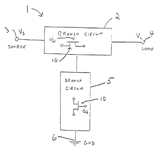
The variable attenuator of the invention is shown
in a schematic block diagram in Figure 2 in which the
attenuator 1 includes a first branch circuit 2 coupled to
a source terminal 3 and a load terminal ~. The attenuator 1
also includes a second branch circuit 5 coupled to the first
25 branch circuit 2 and a common terminal 6, shown in the
illustrative embodiment of Figure 2 as ground. Each of the
first and second branch circuits 2 and 5 include a voltage
controlled variable FET resistor 10.
The voltage controlled variable FET resistors 10 of
30 the present invention have a flexibility in design to allow
the selection of any channel resistance versus control
voltage relationship desiredO Figure 3 shows a schematic
circuit diagram of the voltage variable FET resistor 10 of
~L3V(~ Z~L
--8--
1 the invention comprisiny a FET network 12 coupled to a
voltage divider network 14. The FET network 12 includes an
input terminal 16 and an output terminal 18. The voltage
divider network 14 is coupled to a voltage control terminal
5 20 and to a ground terminal 22.
The FET network 12 comprises a plurality of FET
segments 24 having source (S), drain (D) and gate (G)
electrodes. The FET segments 24 are designated Ql' Q2'
Q3...Qn and have source, drain and gate electrode designed
1' 2' s3 sn; Dl, D2, D3...Dn; and Gl, G2, G3...G ,
respectively. The number, n, of FET segments in the FET
network 12 is determined in accordance with the particular
application and desired voltage-resistance relationship of
the FET resistor 10.
Each of the FET segments 24 in the FET network 12
are coupled in parallel across their respective source and
drain electrodes. Accordingly, all the source electrodes Sl,
S2, S3... Sn are coupled together to output terminal 18, and
all the drain electrodes Dl, D2, D3.-- Dn are coupled
20 together to input terminal 16.
The voltage divider network 14 includes a plurality
of fixed resistors 26 coupled to the gate electrodes of the
FET segments 24 between control terminal 20 and ground
terminal 22. The gate electrodes Gl, G2, G3~.. Gn are
25 coupled to the voltage divider network 14 at nodes Nl, N2,
N3... Nn. Resistor Rl of the plurality resistors 26 is
coupled between node Nl and N2. Similarly, resistor R2 is
coupled between nodes N2 and N3 and resistor R3 is connected
between nodes N3 and N4. Resistor Rn is connected between
30 node Nn and ground terminal 22.
As stated above, a field effect transistor
operating in the linear range of its I-V characteristic curve
acts as a voltage controlled variable resistor. The
3L3VV~:2~
1 resistance measured between the source and drain electrodes
varies in accordance with the voltage applied to the gate of
the transistor. In addition, the range of resistance values
is dependent upon manufacturing parameters and in particular,
5 the width of the gate of the FET. Each of the FET segments
24 in the network 12 have a predetermined gate width
resulting in a predetermined channel resistance measured
between the source and drain of each FET segment. The FET
network 12 includes at least two or more FET segments 24 in
10 which the gate width of at least one of the FET segments 24
is different from the gate width of at least one other of the
FET segments 24.
The FET segments 24, are connected in parallel and
therefore the resistance of the FET resistor 10 measured
15 between terminals 16 and 18 is the equivalent resistance of
the FET segments determined by the parallel resistance
formula:
1 = 1 + 1 + 1 +...+ 1 (2)
RDS RDSl RDS2 RDS3 RDSn
A control voltage VG applied to the control terminal 20 will
be divided by the voltage divider network 14 to provide a
different voltage to each of the gates of the FET segments
24. The individual gate voltages are designated Vl, V2,
V3... Vn, where Vl equals VG. The individual gate voltages
can be derived directly by using the voltage divider formula
VG x (Ri + Ri+l +---+ Rn)
Vi = ~ (3)
Rl+R2+R3+ +Rn
where i = 1, 2, ... n
~3V~2~
-10-
1 As a result of the different gate voltages applied
to each of the FET segments 24, each FET segment 24 wil1 have
a different relationship between VG and the resistance
measured between the source and drain of each FET segment 24.
5 Since the source and drain terminals of each of the FET
segments 24 are connected in parallel, the resulting
resistance of the complete voltage variable FET resistor 10
can be made to match a specified relationship by changing the
number of FET segments 24, the width of each of the FET
10 segments 24 and the voltage divider network 14 resistance
values.
Referring now to Figure 4, the voltage variable FET
resistor 10 is shown in monolithic Eorm. The plurality of
FET segments 24 are formed on a semiconducting substrate,
15 such as GaAs from electrodes having an interdigitated
construction. In the illustrative monolithic embodiment of
Figure 3, the FET segment Q1 is shown with a gate width 2W1.
FET segment Ql is a split FET which is made of two segments
F1 and F2 coupled to the same metal strip thus connecting the
20 two segments in parallel. The effective gate width of FET
segment Ql is equal to the gate width of segment F1 plus the
gate width of segment F2. FET segment Q2 and Q3 have a gate
width of W2 and FET segment Q4 has a gate width W4.
Resistors R1, R2, R3 and R4 are connected as shown to the
25 gates of FET segments Q1-Q4' between control terminal contact
pad 20 and ground terminal contact pad 22. The drain
electrodes of the FET segments Ql-Q4 are connected to input
contact pad 16 and the source electrodes of the FET segments
Ql-Q4 are connected to output terminal contact pad 18.
In implementing the invention, the desired voltage-
resistance relationship necessary for a particular
application is first determined. The desired relationship
~L3~02;~
--11--
1 may be based on the need to have the resistance between the
input and output terminals of the FET resistor 10 vary in a
particular manner upon the application and change of the
control voltage VG. By using a combination of the known
5 equivalent parallel resistance formula and the voltage
divlder formula of equation 3, one skilled in the art can
determine the number of FET segments of the FET network 12,
the required gate width for each of the FETs and the
resistance values for the voltage divider network 14 to
10 construct a voltage controlled variable FET resistor having
the desired voltage-resistance relationship. A computer
simulation program may be used to simulate the
resistance-voltage relationship of FET resistor 10 for
various combinations of gate widths and fixed resistor
values to assist in ascertaining the optimal combination.
The following is a table of values for the
implementation of the FET resistor 10 of the invention shown
in Figure 4.
TABLE
RESISTANCE GATE WIDTHS
Rl = 4.5 k ohms Wl = 110 microns (2 x 55)
R2 = 1.9 k ohms W2 = 40 microns
R3 = 1.7 k ohms W3 = 40 microns
R4 = 1.6 k ohms W4 = 35 microns
Figure 5 is a graph showing the relationships
between voltage and channel resistance for each of the
individual FET segments Q1-Q4 For a control voltage in the
30 range of 0.0 to -5.0 volts, the resistance for each FET
segment varies in accordance with each of the plots shown.
The size of the gate width affects the channel resistance in
~3~
-12-
l a manner such that a larger width will produce a smaller
resistance. As the channels are coupled in parallel, in
accordance with Ohms Law, a smaller parallel resistance will
have a larger contribution to the equivalent resistance. The
5 resistors of the voltage divider 14 determine when each FET
segment will reach pinch off state. Once a FET segment
reaches pinch off, the resistance becomes very large and no
longer contributes to the equivalent resistance. As shown in
Figure 5, between 0.0 and -1.0 volts, all four of the FET
10 segments have values that contribute to the equivalent
resistance. However, between -3.0 and -4.0 volts, only Q3
and Q4 contribute and between -4.0 and -5.0 volts only Q4
will contribute. Figure 6 is a graph showing the equivalent
resistance of the complete FET resistor 10 as a function of
15 the control voltage. Thus, in accordance with the invention,
the relationship between the resistance measured between the
output and input terminals and the control voltage may be
determined by varying the number of FET segments, the gate
widths of the FET segments and the gate voltages applied to
20 the FET segments.
The flexibility in design of the voltage controlled
variable FET resistors 10 permits the variable attenuator of
the invention to have almost any chosen relationship between
the attenuation and the control voltage. Referring again to
25 Figure 2, a signal with amplitude Vs is applied to source
terminal 3. The attenuator l decreases the signal's
amplitude and the signal will emerge from the load terminal 4
with an amplitude VL. The ratio Vs/VL is the attenuation
ratio. The control voltages VGl and VG2 change the
resistances of the FET resistors 10 and thus control the
attenuation ratio and the input and output impedances of the
attenuator. The input and output impedances must be matched
~3V~
-13-
for the attenuator to operate properly within the device in
which the attenuator is employed.
As stated above, the variable attenuator of the
invention may be configured in any topology, such as T, PI or
5 bridged T. The relationship between the attenuation ratio
and the control voltages VGl and VG2 applied to the FET
resistors lO is directly related to the relationship between
the resistance of the FET resistors and the control voltages.
The network equations for the T, PI and bridged T
0 configurations are well known to any one skilled in the art.
By these equations it is known that the attenuation is a
function of the resistor values of the attenuator. Since the
resistor value of the FET resistors lO is a function of the
control voltage, it follows that the attenuation is also a
15 function of the control voltage. To achieve a desired
relationship between the attenuation and the control voltage,
the desired relationship between the channel resistance of
FET resistors lO and the control voltage is determined.
Figures 7, 8 and 9 are schematic diagrams of the
20 variable attenuator of the invention implemented in the
bridged T, T and PI topologies, respectively. Figure 7 shows
a bridged T attenuator 30 in which the first branch circuit 2
includes a first voltage variable FET resistor 10, designated
Zl and two balancing resistors 32 and 34. The two balancing
25 resistors are connected in series between the source and load
terminals 3,4. In order to have a reciprocal attenuator, the
resistors 32 and 34 must be of equal value. The input
terminal 36 of the first FET resistor Zl is coupled to the
source terminal 3 and the output terminal 38 of the first FET
resistor, Zl is coupled to the load terminal 4. The second
branch circuit 5 includes a second voltage variable FET
resistor lO, designated Z2' having an input terminal 40
3l3~ 2~
1 coupled to a node 42 between the two balancing resistors 32,
34 and an output terminal 44 coupled to the common terminal
6.
The variable attenuator 50 of Figure 8 is shown in
5 a T configuration wherein the first branch circuit 2 includes
first and second voltage variable FET resistors 10,
designated Zl and Z2 coupled in series between the source and
load terminals 3,4. The input terminal 52 of the first FET
resistor Zl is connected to the source terminal 3. The
10 output terminal 54 of the first FET resistor Zl and input
terminal 56 of the second FET resistor Z2 are connected
together at a node 58. The output terminal 60 of the second
FET resistor Z2 is coupled to the load terminal 4. The
second branch circuit 5 includes a third voltage variable FET
15 resistor 10, designated Z3 having an input terminal 62
coupled to the node 58 and an output terminal 64 coupled to
the common terminal 6.
The variable attenuator 70 of Figure 9 is
configured in a PI topology wherein the first branch circuit
20 2 includes a first voltage variable FET resistor 10,
designated Zl having an input terminal 72 coupled to the
source terminal 3 and an output terminal 74 coupled to the
load terminal 4. The second branch circuit 5 includes second
and third voltage variable FET resistors 10, designated Z2
25 and Z3, coupled in parallel. The input terminal 76 of the
second FET resistor Z2 is coupled to the source terminal 3
and the input terminal 78 of the third FET resistor Z3 is
coupled to the load terminal 4. The output terminals 80 and
82 of the second and third FET resistors Z2 and Z3 are both
30 coupled to the common terminal 6.
In operation, as stated above, an electrical signal
of amplitude Vs is entered upon the input 3 of each of the
attenuators of Figures 7, 8 and 9. The attenuators decrease
~15-
1 the signal's amplitude and the signal emerging from load
terminal 4 has an amplitude VL. The attenuation ratio VL/Vs
determines the attenuation in db. By convention, the
attenuation in db is equal to 20 log VL/Vs. A 20 db
5 attenuation provides for an output signal VL that is 10
percent of the input Vs. A 40 db attenuation provides an
input signal one percent of Vs and a 60 db attenuation
provides an output signal .1 percent of Vs. For each of the
attenuators of Figures 7, 8 and 9, the control signal VGl is
10 adjusted to change the attenuation while the control signal
VG2 is adjusted to maintain a match of the input impedance ZS
and the output impedance ZL to the system's characteristic
impedance. The adjustments are made using the known
attenuator network equations and the equations governing the
15 resistance of the voltage variable FETs 10.
In one illustrative embodiment of the invention,
the bridged T configuration attenuator 30 is provided with a
linear relationship between VGl and the attenuation ratio,
while keeping matched impedances on both the input and
20 output. The attenuator 30 is shown in Figure 10 implemented
in monolithic form. The voltage controlled variable FET Zl
of bridged T attenuator 30 is identical to the monolithic FET
resistor shown in Figure 4. The second voltage controlled
FET resistor Z2 is shown as having two FET segments Q5 and Q6
25 each having a gate width of W5 of 125 microns. The resistors
for the voltage divider network of the FET resistor Z2 are
shown as R5 and R6. The balancing resistors 32 and 34 are as
indicated. In this embodiment R5 is equal to 1 k ohms and R6
is equal to 2.8 k ohms. For a controlled voltage VGl
30 adjusted from 0.0 volts to ~5.0 volts, a linear attenuation
results as shown in Figure 11. The attenuation varied
linearly from 2 db to 15 db. The return loss is also shown
in the graph of Figure 11. The return loss is a measure of
the impedance mismatch by measuring the power reflected back
~3~Z~
-16-
to the input. The return loss as shown in Figure ll is well
within the acceptable range for attenuators.
~; 5 The voltage variable attenuators of the invention
are particularly useful in the microwave frequency range, but
may also be used in low frequency ranges. The MMIC voltage
variable attenuator of the invention features over a lO db
attenuation range, within the DC to 12 GHz frequency band
lO where the attenuation varies linearly with the control
voltage. The linearity of the attenuators makes them
particularly appealing ror applications such as temperature
gain compensation of GaAs FET amplifiers.
While illustrative embodiments of the subject
15 invention have been described and illustrated, it is obvious
that various changes and modifications can be made therein
without departing from the spirit of the present invention
which should be limited only by the scope of the appended
claims.
;
3o