Note: Descriptions are shown in the official language in which they were submitted.
~3(DO;~82
70128-131
WIRE BONDS ~ND ELECTRICAL CONT~CTS OF ~N
INTEG~TED CIRCUIT DEVICE
Jon Long
BACKGROUND OF THE INVENTION
Field of the Invention
.
This invention relates to IC devices and in particular
to the formation of wiring connec-tions of integrated circuits.
Description of the Prior Art
During manufacture of IC devices, the circuit elements
are formed on a die, and the IC die assembly is joined to a die
attach pad, typically by an epoxy adhesive. Electrical lead wires
are bonded to contact points of the IC device by bonding to
conductive elements or fingers and/or with the die attach pad.
The lead wires in turn are coupled to external circuitry for
processing data and control signals.
During the attachment of the IC die to the die attach
pad, the epoxy adhesive which is made with a resin tends to bleed
and flow along the surface of the pad beyond the area of joinder
of the die and the pad. The flow of resin makes it difficult to
properly bond the lead wires to the conductive die attach pad.
~ith prior art processes, it is necessary to exercise stringent
control of the application of the adhesive material while it is
being dispensed. Furthermore, limitations on the chemical
properties of the adhesive are imposed. As a result, the problem
of lead wire bonding becomes time-consuming and costly.
- ~L3~ 8:~
70128-131
An additional problem associated with making wire
connections is the possibility of electxical shorting to -~he die
attach pad that may occur during the bonding of the lead wires to
the lead fingers, which requires ex-tra care and testing during
production. The die attach pad is made of an electrically
conductive material, such as copper. The noninsulated lead wires
when bonded to the lead fingers can inadvertently make contact
with the conductive die attach pad, thereby creating an electrical
shorting condition.
Also, during the mass production of IC devices, a
multiplicity of lead wires are connected by means of automated
bonding equipment to electrical contact points and bonding pads.
Prior production techniques relied on an operator to designate
the lead area visually, and a computer to provide alignment of the
contact points that are to be bonded by bonder apparatus having
capillaries for providing the bonding material. As a result of
the dramatic increase in the number of lead wires which are used
with IC devices and the limitations of size and space provided
between the components of an IC device, the lead wires by
necessity are very closely spaced, thus requiring very accurate
and precise bonding in order to avoid erratic connections and
electrical shorting. Therefore, during the bonding process, it is
necessary to align the capillaries of the bonder apparatus
precisely relative to the electrical contact points on the bond
pad of the die attach pad of the IC assembly.
70128-131
Furthermore, with a composite rigid frame and flexible
tape assembly, such as discussed below, it has been observed that
when the IC device is subjected to a high temperature, such as
occurs during vapor phase assembly which èmploys a temperature
greater than 21~ Centigrade for example, or during heat testing,
a "clam shell" effect occurs. This clam shell effect causes the
iead fingers or wires of the IC assembly tG bow or separate so as
to distort the planar elements of the IC device, which makes the
device unusable.
Another problem that may occur as a result of the
production process is the delamination of the Kapton layer that
secures the lead fingers of the frame and tape assembly. During
manufacture of an IC device using the frame and tape assembly, an
insulating film made of a material such as Kapton la trade-mark of
DuPont Corp.) is deposited on the flexible tape-like structure.
The Kapton film serves to secure the thin flexible conductive
leads formed with the tape-like structure, and electrically
insulates the leads from each other. Kapton material is subject
to becoming brittle in the presence of moisture. Also, a
continuous film of Kapton has a tendency to delaminate from the
tape-like structure.
~UMMARY
An object of this invention is to provide an integrated
circuit (IC) assembly wherein the problems associated with the
assembly of the electrical leads of the inteyrated circuit
assembly are effectively eliminated.
~3~
70128-131
Another object of this invention is to provide an IC
device wherein the bonding of lead wires between the IC hip and
the electrical contact points of a bond paid of the IC assembly is
facilitated.
Another object is to provide an IC device wherein
electrical shorting of the electrical leads to the die attach pad
is effectively minimized.
A further object is to provide an IC device wherein
structural distortion that may result when the IC device is
subjected to high temperatures is avolded.
According to one feature of this invention, a dam made
of insulating material is formed on the die attachment pad to
encompass the IC die structure. The dam limits the flow of resin
of the epoxy adhesive, which is used for attaching the IC die to
the die attach pad, and the resin is contained within a cavity
formed between the dam and the die.
Another feature of this invention is the provision of an
insulator ridge which ensures that the bond wires remain spaced
from the conductive die attachment pad to preclude electrical
shorting.
An additional feature of this invention is the provision
of a recognition pattern at specified locations on the flexible
tape like structure. The pattern is sensed by an optical sensor,
for example, to generate signals that are directed to a computer
actuated bonder, which is aligned accurately with the electrical
connection points on the bond pad of the IC assembly.
-
2~
70128-131
A further feature of this invention is the provision of
an insulating molding material that is interposed in cavities
between the Kapton layer to ensure that the lead fingers of the
composite frame and tape assembly are securely held.
DESCRIPTION OF THE DRAWING
The invention will be described in detail with reference
to the drawing in which:
FIG. 1 is a top plan view of a support assembly for an
IC chip;
FIG. 2 is an enlarged side sectional view of a support
assembly for an IC chip, which incorporates a flexible tape-like
structure and rigid lead frame assembly;
FIGS. 3a-d are sectional side views of portions, broken
away of the support assembly, illustrating the dam and wedge
structures embodied in the inventive structure;
FIG. 4 is an enlarged sectional view of a portion of a
support assembly for an IC chip, incorporating the dam and wedge
structures and additionally a recognition pattern, as employed
with this invention;
FIG. 5 is a sectional view of a portion of a support
4a
CHP/M-442 1~28~
1 assembly for an IC chip, incorporating the feature of using
2 a molding compound in cavities between Kapton material to
3 secure the lead fingers of the assembly, in accordance with
4 this invention; and
FIG. 6 is a representational sectional view of a
6 package including the frame and tape assembly which
7 incorporates the novel features of this invention.
8 Similar numerals refer to similar elements throughout
g the drawing.
11 DETAILED DESCRIPTION OF THE INVENTION
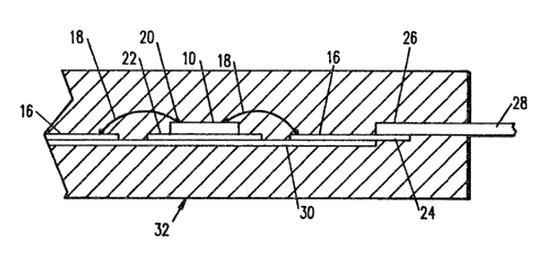
12 With reference to FIGS. 1 and 2, an IC assembly
13 comprises an IC chip 10 that is mounted to a die attach pad
14 22. Bond wires 18 are connected at one end to the surface
1~ of the IC chip device and at the other end to lead fingers
16 16. The outer portions 24 of the lead fingers 16 are in
17 electrical contact with lead bonds 26 which extend from the
18 enclosing package 32 to provide package leads 28. The
19 package leads 28 are connectable to conductive leads or
wires that are provided by external circuitry. In this
21 manner, the integrated circuit has a conductivè path through
22 the IC package to external circuits for the transfer and
~3 exchange of data signals.
24 During the attachment of the IC die 10 to the die
attachment pad 22 employing conventional semiconductor
technology, an epoxy adhesive formed with resin is used. As
27 is well known, the resin in the epoxy has a tenden~y to flow
28 during the process of joining the die and the pad. The
resin tends to flow towards the down bond channel 44 which
has a number of electrical contact points to which wire
3 ` leads, such as leads 46 and 48 in FIGS. 3a and 3b, are
31 bonded. The wires 46 provide connec-tion from the die attach
32 pad to the inner lead fingers 16 and thus to an external
33 control for supplying voltage to the IC die attachment
34 pad. Wires 48 provide connection from the die attachment
pad to the IC chip 10 whereby the IC device controls the
36 polarity of the die attach pad. However, the presence of
37 resin that flows from the adhesive makes it difficult, if
38
-- 5 --
CHP/M-442 ~0~28~
1 not impossible, to make a secure bond between the wire leads
2 and the electrical contact points in the down bond area.
3 To avoid the deleterious effect of the resin bleeding
4 from the epoxy adhesive over the down bond channel 44 of the
die attach pad, a dam 42 that circumscribes the IC die 10 is
6 provided, as shown in FIG. 3a. The dam is formed on the
7 surface of the die attach pacl and is spaced close to the
a periphery of the IC die. The dam is formed preferably of
g Kapton ~trademark of Du Pont) which is an insulating
material. The dielectric Kapton material forms a continuous
11 wall or barrier and acts effectively to impede the flow of
12 the resin across the surface of the die attach pad and to
13 contain the resin between the IC device 10 and the dam. As
14 a result, when lead wires are attached to the die attach pad
at the down bond channel, the resin does not interfere with
16 the attachment of the ends of wire leads 46 to the contact
17 points on the surface of the pad 22, or of wire leads 48.
18 In accordance with another feature of this invention, a
19 wedge S2 is provided between the die attach pad 22 and the
lead fingers 16 so that the lead wires 50 from the IC device
21 10 to the lead fingers 16 are prevented from contacting the
22 die attach pad 22. As illustrated in FIGS. 3c and 3d, the
23 wedge 52 is formed at the area between the pad 22 and the
2~ lead finger 16 and is so positioned as to maintain the
desired separation of the wire 50 from the pad. The wedge
26 52 may be made of Kapton or of any dielectric material that
can be formed to the desired wedge shape.
28 With reference to FIG. 4, a recognition pattern 54 is
incorporated in the corners of the tape-like structure 14 to
enable alignment of electrical contact points 56 of the down
bond channel and contact points 58 for precise bonding of
the IC device to the inner lead fingers 16 by an automated
32 X-Y bonder. As it is necessary to align the capillaries of
33 the bonder from which bonding wire material is ejected to
34 the contact points at which wire leads are connected very
accurately, the recognition pattern serves as a target to
36 enable precise alignment. The recognition pattern is
37 characterized by providing pairs of spaced geometric
38
-- 6 --
CHP/M-442 ~30028~
1 elements, which are illustrated as being rectangular in this
2 embodiment, that are formed by etching a specified design on
3 the metal layer of the tape structure 14. The spaced
4 elements of one pair define a first axis and the spaced
elements of a second pair define an axis different in
6 direction than the first axis. The spaced elements include
7 components that are collinear and aligned along one axis or
8 direction and at least two other collinear components
g aligned along a second axis, preferably at 90 to the first
axis. An optical scanner scans along the linear direction
11 provided by the edges of a pair of components of the pattern
12 and if the edges are not scanned in precise alignment, an
13 error signal is generated which is fed to a computer. The
14 computer then adjusts the X-Y position of the automated
bonder so that it is properly aligned with relation to the
16 contact points that are to be bonded.
17 FIGS. 4 and 5 illustrate another feature of this inven-
18 tion which is directed to the wire leads of the IC tape
19 structure and frame assembly. During manufacture of the
tape assembly, an insulating film ~ preferably made of
21 Kapton is deposited over the tape-like structure 14 to
~2 secure the thin flexible lead fingers 16 and to provide
23 insulation between the individual leads. The insulating
24 film ~ is etched to produce cavities 62 that are interposed
between the remaining unetched sections of the insulating
2 Kapton film. The assembly including the tape lg, the frame
27 12 and the etched Kapton film with the cavities is housed in
a plastic package 32, as is well known in the industry. In
keeping with this invention, an epoxy molding compound is
then forced through an aperture of the package mold to form
3l the plastic package. The molding compound flows into the
32 cavities between the Kapton sections~ The molding compound
effectively locks around each conductive lead to provide
33 electrical insulation and to secure the thin flexible lead
34 fingers firmly in place.
The use of the epoxy molding compound effectively
36 lowers the moisture penetration, and since the Kapton is
37 known to be sensitive to moisture and tends to become
38
-- 7 --
CHP/M-442 1~00282
1 brittle, the partial substitution of the molding compound
2 minimizes problems that were encountered with a continuous
3 complete layer of Kapton. Furthermore, the problem of
4 delamination, which a continuous film of Kapton can
experience, is substantially eliminated. Also, by having
6 the cavities filled with molding compound, the detrimental
7 effects of clam shelling is reduced.
11
13
l4
16
19
22
24
26
28
32
37
38