Note: Descriptions are shown in the official language in which they were submitted.
3 30CJ~;~OO FJ, AC- 7 0 0 6
-- 1 --
CONNECTOR APPARATUS FOR HIGH DENSITY
COAXIAL CABLES
BACKGROIJND OF THE INVENTION
1. Field of the Invention
The present invention relates to a connector
for a high densi y cable, more particularly, it relates
to a mechanism for connecting a coaxial cable to a
printed circuit board through an associated latch, the
connectors being located on the printed circuit board in
a matrix arrangement and at a high density.
Due to a current requirement for an increased
density of connectors mounted on a printed circuit board
(reerred to as PC board hereinater), a matrix mounting
system in which a desired number of contact pins is
; grouped into a block, and a plurality of connectors axe
located in a matrix arrangement corresponding to the
desired number of contact pins, is used. Xn this matrix
mounking system, however, beaause the number of
connectors i~ incrQased the lat~h means must be improved
to prevent interference between conn0ctors located very
close to ~ach othex, in order to increase the mounting
density thereof, in a very small mounting space.
2. Description of the Related ALt
In known connectox latch means/ the connectors
are individually secured to the PC board by set screws,
or connectors in the same row of a matrix are latched
~5 together. The coaxial cables to be connected to the
respective connectors are provided with grounding
shields, and the shield connection is made by mating
special grounding contacts and the contact pins by
plugging them together.
The conventional latching method mentioned
above has drawbacks in that it is very difficult to
mount and dismount the connectors and that the latching
means is large and complex, and thexefore, preferably a
~3(~
2 -
simple latching means is provided for each connector, by
which an effective utilization can be made of a very small
mounting space. Note, the plug-in shield connection of the
cable allows an increased number of contact pins and an
increased number of patterns of the PC board to be used.
Preferably, the shield of the cables is directly connected
to a frame of a housing of the associated apparatus, to
ground same. In this case, preferably the connectors them-
selves are grounded to prevent a generation of static elec-
lo tricity when an operator accidentally touches the connectors
during the mounting and dismounting thereof.
SUMMARY OF THE INVENTION
A feature of one embodiment of the present invention is
to provide connectors for high density coaxial cables by
which the shield connection of the cables is optimized by
providing a one-touch type latch means for each connector.
In accordance with an embodiment of the present inven-
tion there is provided an apparatus for connecting a high
density cable assembly to be connected to corresponding
contact pin~ pxovided on a substrate having guides, each
guide having a predetermlned number of aontact pins therein,
comprising a connector to whiah the cable assembly is con-
nected and which is to be mounted on the associated guide,
said connector having a connector body guided by the asso-
ciated guides and a connector cover surrounding the con-
nector body, and latching means rotatably mounted between
the connector body and the connector cover, for latching the
connector to the associated guides and wherein electrical
shielding of the cable assembly is ef~ected by the guides
and connector cover.
With this arrangement, a plurality of connectors each
having the latching means can be easily and quickly latched
and unlatched to and from the associated guides. The
shields of the cables are grounded through the guides.
7~)~
-- 3 --
Preferably, the latching means comprises a
rotatable latching lever for latching and unlatching the
connector to and from the associated guides by a
one-touch operation.
Also, preferably, the latching lever is provided
with hooks, and the guides are provided with corre-
sponding abutments with which the associated hooks can
engage. The latching lever is rotatably supported by
and on the connector cover in such a manner that a
rotation of the latching lever causes the cover to be
latched and unlatched to and from the associated guides.
BRIEF DESCRIPTION OF T~E DRAWINGS
The invention will be described below in detail
with reference to the accompanying drawings, in which:
Figure 1 is a partially sectioned side
elevational view of a connector apparatus according to
an aspect of the presenk invention;
Fig. 2 is a plan view of a mother board having
guides in a matrix arrangement shown in Fig. 1;
Fig. 3 i9 a partially broken perspective view
of a connector apparatus shown in Fig. l;
Figs. 4~ and 4~ are a front elsvational view
and a partiall~ sectioned side elevational view o~ a
connector cover ~hown in E'ig. 1;
Fig. 5 ls a perspective view of a latching
lever according to an aspect of the present invention;
Fi~. 6 i~ ~ view showing consecutive steps of
connecting a connector to a substrate, according to the
present invention;
Fig. 7 is a partially sectional side eleva-
tional view of a connector according to the present
invention;
Figs. 8 and 9 are front and side elevational
views of a contact assembly shown in Fig. 7,
respectively;
Fig. 10 is a perspective view of a connector
apparatus having an individualizing means, according to
... . . . . . ... . . ...
.
-- 4 --
the present invention;
Fig. 11 is a schematic view of a matrix
arrangement of connecting portions defined by guides,
according to the present invention;
Fig. 12 is a perspective view similar to
Fig. 11, but showing another embodiment of the individu-
alizing means;
Fig. 13 is a perspective view of a jig which
can be used to mount and dismount a connector to and
from a substrate;
Fig. 14 is a perspective view of the jig shown
in Fig. 13, in which the jig is disconnected from a
connector;
Fig. 15 is a side elevational view showing how
to operate clamping levers of the jig; and,
Fig. 16 is a side elevational view of Fig. 15
showing how to operate an unlocking lever of the jig.
DESCRIPTION OF THE PREFERRED EMBODIMENTS
Referring to Figures 1, 2 and 3, a printed circuit
board (PC board) 2 has IISI's 100 mounted thereon on one
surface (lower surace in the illustrated embodiment) of
a mother board (substrate) 1 by connectors 8, and on the
surface o~ the mother board 1 opposite to the PC board 2
(which can be a substrate in the absence of the mother
board) a yrounded frame 3 is provided in parallel with
the plane of the mother board. The mother board 1 is
attached to a housing frame 6 by mounting frames 4 and
L-shaped mountings 5. The grounded frame 3 is connected
to the frame 6 by a connecting means 7, to form an
electrical shielding circuit.
A number of contact pins 10 corresponding to the
I,SI~s 100 are provided on the side of the mother board 1
~ close to the grounded frame 3. The contac~ pins 10 are
-~ divided into groups of a predetermined number of the
contact pins 10, in a grid-like arrangement, by
guides 11. The guides 11 are made by metal die casting
and are taller than the contact pins 10. The guides 11
- . . . , . .. . ~......... . ..
~L3~07~
-- 5
are held by the mounting frame ~ in such a manner that a
clearance exists between the guides 11 and the mother
board 1; and so that the guides 11 per se are grounded.
Connecting portions 12, defined by the guides 11 to form
a matrix, are connected by a plurality of connectors 20
which extend through corresponding openings 13 of the
grounded ~rame 3.
As the connectors 20 are identical, the following
description is directed to only one of the
~o connectors 20, with reference to Figs. 3 and 4A and 4B.
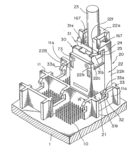
The connector 20 has a generally rectangular box-like
connector body 21 containing contacts to be connected to
a~sociated contact pins lO in a plug-in manner. The
connector body 21 can be loosely inserted in the
associated guide 11 before the final connection with the
contact pins 10. The connector body 21 is provided with
a rectangular box-like metal cover 22, which preferably
consists of two parts 22A and 22B secured to each other
b~ set screws 73, surrounding the periphery of an upper
part of the connector 20. Namely, the lower park of the
connoctor bod~ 21 is not covered by the cover 22, as can
be s~en Erom Fig. 4A. The hoight o~ khe uncovered area
oE t~e connector body 21 depends on the height of the
guides 11~ The front cover part 22A is provided at the
2S upper end thereo~ with a cable mounting portion 22a
integral therewi~h, so that a shield 23a of an
associated coaxial cable assembly 23 having a plurality
of coaxial cables is held by a clamp 24 secured to the
cable mounting portion 22a by screws 25 and connected to
the cover 22. The cover 22 is provided at the upper end
thereof with an opening 22c located below the cable
mounting portion 22a and having a stepped stop 22b. A
latching means 30, described hereinafter, is provided in
the opening 22c.
The latching means 30 includes a generally inverted
U-shaped (gate-like) latch lever 31 made of metal, as
shown in Fig. 4. The latch lever 31 has right and left
., . . . .. , . ~ . .
130(~700
- 6 ~
legs 31a having tapered hooks 31b, which are bent
outward, at the lower ends thereof. The legs 31a are
also provided with pin holes ~lc at an intermediate
portion thereof. The upper ends of the legs 31a are
interconnected to form an abutment surface 31d having a
bent grip 31e. The latch lever 31 is also provided with
a bridging portion 31g connecting the leg portions 31a
and having spring arms 31f. The latch lever 31 is
located in the cover 22 in such a way that the grip 31e
is protruded outside thereof through the opening 22c,
the abutmant surface 31d bears against the stop 22b, the
legs 31a extend downward in side recesses 21a formed on
opposite right and left side faces of the connector
body 21, and the hooks 31b are located outside the
cover 22. The latch lever 31 is rotatably supported on
the cover 22 by associated pins (shafts or projections)
22d provided on the inner side faces of the cover 22 and
rotatably fitting in the associated pin holes 31c, to
enable the legs 3la to rotate about the respective
pins 22d. The free ends of the spring arms 31f bear
against an inner projection 22e provided on the cover 22
(rear cover pa~ 22B) to elastically bias the latch
le~er 31 in a count.erclockwise direction (in Fig. 4B),
whereby the legs 31 are held in a vertically extended
position by the stop 22b.
Furthermore, each guide 11 is provided with
abutments 33 defining recesses 32 and having tapered
upper edyes 33a on the right and left side walls lla of
the guide 11. Note that, in the illustrated embodiment,
since one abutment 33 is common to the two ad~acent
hooks 31b of the two adjacent latch levers 30, the
amount p (Fig. 4A) of outward projection of the
hooks 31b is substantially equal to or less than half
the width w (Fig. 3~ of the abutment 33.
Figure 6 shows the consecutive steps (a) to (d) for
connecting the connector 20 to the guide 11 by the
associated latch means 30. In Fig. 6, before the
. :
"` ~3~(37~:~
-- 7
connection, the latch lever 31 of the latching means 30
bears against the stop 22b, so that the leg 31a and the
hooks 31b are vertically extended. From this position,
when the connector 20 is inserted into the associated
guide 11 the plug-in connection begins, and the
hooks 31b of the latch lever 31 come into contact with
the tapered edges of the associated righ~ and left
abutments 33 of the guide 11, as shown in Fig. 6 (b). A
further insertion of the connector 20 causes the
hooks 31b of the latch lever 31 to slide down on the
tapered edges of the abutments 33, thus resulting in an
elastic deformation of the latch lever 31, as shown in
Fig. 6 (c). Namely, the latch lever 31 rotates about
the pins 22d in a clockwise direction in Fig. 4B. Note
that the rotation, i.e. the elastic defoxmation o~ the
legs 31a of the latch lever 31, occurs in a plane
substantially paxallel with the opposite side faces of
the connector body 21. The hooks 31b lie in a plane
parallel with the plane o~ the legs 31a, a~ can be seen
from Fig. ~, and ~caor~ingly, the displacement
(deformation) of the hoo]cs 31b also occur~ in a plane
~ubstantiall~ par~llel with the side faces of the
connector body 21.
When the plug~in connection is completed, i.e. when
the hooks 31b pass the associated abutments 33, the
latch lever 31 is elastically returned to the initial
position thexeof shown in Fig. 6 (a), due to the elastic
bias applied thereto, as shown in Fig. 6 (d), so that
the hooks 31b are snap-engaged by the associated
abutments 33 to lock the latch lever 31 in position, and
accordingly the connector 20, in the guide 11. In the
locked or latched position shown in Fig. 6 (d), the
lower end of the cover 22 comes into contact with the
upper peripheral surface of the guide 11.
Note, when the connector 20 is in the latched
position, the shield 23a of the cable assembly 23 is
connected to the grounded frame 3 through the cover 22,
.. , .... .. . . . . ~
-~ 13W~
-- 8
the latch lever 31, and the guide 11, and therefore, the
shield 23a of the cable, the cover 22, etc., o the
connector 20, and the guide 1~ are directly grounded and
electrically shielded.
Figure 6 (e) shows the latched (or locked) position
shown in Fig. 6 (d), as viewed from the left side of
Fig. 6 td).
When the connector 20 is to be disconnected from
the associated guide 11, the latch lever 31 is rotated
in the counterclockwise direction in Fig. 4B by manual
pressure exerted on the grip 31e by the operator's
finger, to disengage the hooks 31b from the associated
abutments 33. The connecto~ 20 can be then easily
pulled up, to separate the connector body 21 from the
contact pins 10. Note that, when pressure is applied to
the ~rip 31e, the grip 31e is brought into contact with
an end sur~ace (stop sur~ace) 22f of the cable mounting
portion 22a of the cover ~2 to hold the latch lever 31
at an elastically deformed position and thus enable the
disconnection oF the connector 20 from the contact
pins 10.
~ s can be understood from the above descript.ion,
according to the present invention, since each connector
is provided with a lakching means able to be operated by
a one-touch operation, the connectors can be easily and
firmly connected to the P.C. board.
Further, since the latching means 30 which ensure
this connection in cooperation with the associated
guides 11 provided on the mother board 1 are accom-
modated between the connector bodies 21 and theconnector covers 22, the connector mechanism can be made
compact and small.
Also, since the elastic latching means are in the
form of a gate having right and left legs 31a by which
the opposite sides of the associated connectors are
latched, a strong latching effect is obtained.
` Note, the latching means also contributes to a
:
... ... ........
,:
~-3~
.-'. g
prevention of connection ~ailures among a plurality of
the connectors and the contact pins, since the latching
levers 31 are engaged in the corresponding recesses 21a
formed on opposite sides of the connector body 21.
Further, since the shields of the cables are
effectively grounded by the connector covers, etc., the
number of contact pins and patterns for the PC board can
be reduced, as there is no need to provide specific
contact pins for grounding.
Also static electricity is not generated, since the
connector cover, the latch lever and the guides form a
shield circuit which is integrally grounded.
Figures 7 to 9 show the internal construction of
the connector body 21.
In the connectors for the coaxial cable assembly 23
according to the prior art, each of the coaxial cables
(123A, 123~, etc.) in the cable assembly 23 has at least
one signal line and a grounded shield. Accordingly,
wh0n the number o~ the coaxial cables in one cable
20 assembly is increased, the number of corresponding
contacts of the connector body to be connected to the
signal lines and the grounded shield must be increased.
Furthermore, in the prior art, the coaxial cables in the
cable assembly are separate from each other, and
25 accordingly, the assembly thereof is cumbersome.
To solve these problems, according to another
aspect of the present invention, two coaxial cables are
paired and have a common ground, to reduce khe number of
the contacts in the connector body, and thus make it
30 possible to reduce the space (pitch) between the
contacts.
Namely, in any one pair of coaxial cables, one
contact for grounding is provided commonly to the two
coaxial cables of the pair. Preferably, the contacts
for the signal lines are located on opposite sides to
the grounding contact.
As shown in Figs. 7, 8 and 9, the bottom part of
., . , , ., ., . .. , , . ., , ~, ... .
~300~
.
-- 10 --
the connector body 21, the upper part of which is
covered by the cover 22 as mentioned before, is provided
with a plurality of pin insertion holes 103, arranged in
three rows in the illustrated embodiment, and a contact
5 asse~bl~ 110 is located above each pin insertion
hole 103.
The contact assembly llO will be described below in
detail with reference to Figs. 8 and 9.
Each contact assembly llO is provided with a center
lO elongated connecting piece 111 for grounding (referred
to hereinafter as a ground connecting piece) and right
and left short connecting pieces 112 and 113 for signal
lines (referred to hereinafter as signal connectin~
pieces). The signal connecting pieces 112 and 113 are
15 located on opposite sides of and in parallel with the
center ground connecting piece 111, with a space
therebetween. The pieces 111, 112, and 113 are provided
at intermediate portions thereof with recessed
portions lllb, 112b and 113b, and are made integral with
20 each other at the recessed portions lllb, 112b and 113b
by a holder 114, preerably made o~ plastic.
The lower ends o~ the pieces 111, 112, ~nd 113 are
pro~ided with ~orked or bi~urcated contacts llla, 112a,
and 113a lying in a plane, i.e. in a row, and two
25 coaxial cables (e.~., 123A and 123B) are located above
and suhstantially in line with the signal connecting
pieces 112 and 113.
The signal lines 115A and 115B of the cables 123A
and 123B are fixed to upper ends 112c and 113c of the
30 connecting pieces 112 and 113 by heat-shrinkable
` tubings 117. The upper end of the ground connecting
piece 111 extends upward beyond the upper ends 112c
and 113c of the signal connecting pieces 111 and 112 and
is bifurcated to form terminal ends lllc and llld which
are soldered directly to the shields 115b and 116b of
the cables 123A and 123B. The holder 114 is provided
with clamp pin holes 129 located between the xecessed
.. ,.... . ,.. . . ,;;.. . ...... .
,,
1300~00
-- 11 --
portions lllb and ll~b and between the recessed
portions 112b and 113b thereof. Note, the holder 114 is
also provided with a projectipn 118 on one side face
thereof, to enable the operator to differentiate the
front and rear sides of the holder 114.
The connector body 21 is provided with contact
holes 104 directly above the pin inserting holes 103,
stepped portions 105 for accommodating the
projections 118 of the holders 114 pin holes 106, and a
chamber 107 for receiving the contact assembly 110.
When the contact assembly 110 is inserted in the
receiving chamber 107, the pxojections 118 of the
holders 114 are engaged in the stepped portions 105, and
the contacts llla, 112a, and 113a are inserted in the
associated contact holes 104. The other contact
assemblies 110 are similarly inserted in the connector
body 21 in a side by side arrangement, so that the
holders 11~ are brought into contact with each other at
the longit-ldinal opposite sides thereof. Thus, when all
o~ the contact a~semblie~ 110 have been inserted in the
connec~or body 21, clamp pins 119 are inserted in the
pin hole~ 117 through the pin holes 106 to prevent an
acciden~al remo~al o~ the contact assemblies 110 ~rom
the connector body 21.
In this arrangement, when the connector body 21 is
fitted onto contact pins provided on the mother board 1,
the contact pins of the mother board 1 are inserted in
the associated pin insertion holes 103 and the
associated contacts llla, 112a, and 113a and connected
thereto in a plug-in manner.
In the arrangement shown in Figs. 7 to 9, two
coaxial cables 123A and 123B are paired and provided
with a common ground, and accordingly, theoretically the
number o~ ground contacts can be cut by half, and thus a
small and compact connector mechanism having a reduced
pitch of the contacts can be obtained.
Note, the arrangement of the signal lines on
'
.. .. . . . . . . . . . . . .
~3V~t7~
~ 12 -
opposite sides of the ground line contributes to a
reduction of noise, and since the cables are soldered to
the corresponding signal connecting pieces substantially
in a straigh:t line, damage to the cables can be reduced.
Figures 10 and 11 show an embodiment direc-ted to a
prevention o~ a faulty connection between the connectors
and the contact pins on the mother board 1 ~PC board 2),
according to another aspect of the present invention.
As shown in Figs. 10 and 11, the connector cover 22
of the connector 20 is provided with downwardly
extending tongues 127 which serve as a bar code, as
often used, for e~ample, in a POS (Point Of Sales)
system. Namely, each connector cover 22 is provided on
one side thereof with a tongue or tongues 127, as can be
seen from Fig. 10. The positions of the tongues of
adjacent connectors 20 are different from each other, to
provide each connector 20 with an individual identify.
Namely, as can be seen in Fig. 10, the tongues 127 of
the adjacent connectors 20 are located in different
position~. Alternatively, a plurality o~ tongues 127
can be provided on each connector 20, and these
tongues 127 will functiorl as a bar code as used in a POS
system, as shown in Fig. 12.
; The gui~s 11 are provided with recesses 141 on the
side walls thereoE corresponding to the tongues 127 o
the associated connectors 20, as shown in Fig. 10.
Consequently, only connectors 20 having tongues 127
corresponding to the recesses 141 oi the guides 11 can
be inserted in the associated guides 11. Namely, if a
connector 20 is inserted in an incorrect guide 11, the
tongue or tongues 127 will not fit in the recess or
recesses 141 of the incorrect guide 11. Further, since
the tongue 127 is provided on only one side o the
cover 22 of the connector 20, the direction (right side~
left side, front side or rear side) of the connector
cover 22 can be easily and visually determined by the
engagement of the tongues 127 and the recesses 141.
. . . ~ . . .
.
::,. ......... . .
.. ...
3 - 13~$~
Alternatively, the tongues (male members) 127 and
the recesses (female members) can be provided on a side
wall of the guides 11 and one side face of the connector
cover 22, respectively.
Further, the tongues 127 can be of different
widths, to provide individuality to the connectors 20.
Furthermore, the tongues 127 can be provided on two
or more adjacent or opposite side faces of the connector
covers 22 or the side walls of the guides 11.
In particular, when one tongue is provided on one
connector cover (or on one guide wall), preferably
identical connectors having a plurality of tongues 127,
the number of which corresponds to the number of kinds
of tongues, are manufactured so that, when the
connection of the connectors to the contact pins
provided on the mother board 1 ti.e., the PC board) is
to be made in accordance with a specific design, only
one tongue is kept and the other tongues are removed.
This provides an increased mass-productivity and an
easier maintenance o such identical connectors.
Figure 11 shows a practical matrix arrangement of
the connectors, as an example.
The four connecting portions 12 (12a~ 12b, 12c,
and 12d) of the mother board 1 form one block B, and a
number of blocks B are arranged in a matrix on the
mother board 1. As seen in the block B shown in
Fig. 11, the guides lla, llb, llc, and lld of the four
connecting portions are provided with the recesses 141a,
141b, 141c, and 141d at different positions, and the
four associated connectors 20 (not shown in Fig. 11) are
provided with the tongues 127 at positions corresponding
to the associated recesses 141a, 141b, 141c, and 141do
The combinations of numerals 1 to 4 in the matrix
arrangement in Fig. 11 are different at each block B.
As can be seen from the above description,
according to the present invention, since the connectors
can be given addresses and orientations (directions) by
~070(3
, ..~
- 14 -
the male (tongue) and female (recess) address allocating
means, a faulty connection or incorrect polarity will
not occur.
Figures 13 to 16 show a special jig 150 for
mounting and dismounting the connector to and ~rom the
; contact pins on the mother board 1 (or the PC board).
This jig is particularly useful when the connectors are
mounted in a high densiky matrix arrangement.
The jig 150 is provided with a shank 151 to serve
as a grip ~or the operator, and a connector unlocking
lever 153 rotatably supported by the lower end of the
shank 151 at a point close to the connector 20, through
a pivot pin 155 extending perpendicular to the length of
the shank 151. The connector unlocking lever 153
rotates in the clockwise direction Al in Fig. 16. After
the ~ig 150 is attached to the associated connector 20,
as described hereinafter, the upper end thereof is
manually pushed close to the shank 151 and the connector
unlocking lever 153 is rotated in the clockwise
direction A~ in Fig. 16, 50 that the lower end 153a o~
the lever 153 is pressed ag~inst the grip 31e (Figs. 4A,
4~, and 5) o~ ~he latching lever 31 to e~ert pressure on
the grip 3le to Inlock ~he hoolcs 3lb of the latching
lever 31 ~rom ~he associa~ed abutments 33 o~ the
guide 11. Note, the hooks 31b can be manually dis-
engaged or unlocked from the associated abutments 33
without using the jig 150, i.e., the grip 31e can be
directly moved by the operator's finger to unlock the
hooks 31b from the associated abutments 33. The
lever 153 is continuously biased in an open position by
a spring 154 provided around the pivot pin 155, in which
the lower end 153a of the lever 153 is held apart from
the associated lower ends 157a of the clamping
levers 157, as can be seen in Fig. 16.
The jig 150 is also provided with a pair of
clamping levers 157 rotatably supported at the lower end
of the shank lS0 by respective pivot pins 159 extending
~3C~ '0~
-- 15 --
perpendicular to the pivot pin 155 and to the length of
the shank 151. The clamping levers 157 are continuously
biased to a closed position by springs 161 provided
between the shank 151 and the levers 157, in which the
lower ends of the levers 157 adjacent to the
connector 20 are brought close to each other. The
clamping levers 157 are opened in the directions A2
(Fig. 15) at the lower end thereof, against the force of
the springs 161, by pressing the upper ends of the
clamping levers 157 toward each other in the
directions A3 in Fig. 15.
The lower ends 157a of the clamping levers 157 are
provided with claws 165 which can be engaged in corre-
sponding clamping recesses or openings 167 (Fig. 3)
formed in opposite sides of the cable mounting
portion 22a of the cable cover 22, when the clamping
levers 157 are in the closed position. When the
clamping l`evers 157 are brouyht to the open position in
which the lower ends 157a of the levers 157 are
sep~rated from each other, the claws 165 of the clamping
levers 157 are engaged Ln th~ associated clamping
openings 167. Nhen t~te external force applied to the
~Ipper ends of the clamping levers 157 in the
direation ~3 is released, the clamping levers 157 are
automatically returned to the closed position, so that
the claws 165 are engaged in the corresponding opposed
clampin~ openings 167 from the opposite sides of the
connector 20, and as a result, the connector 20 is
firmly held by the jig 150, as shown in Fig. 13. Since
the jig 150 substantially has no part projecting outward
from the width of the connector, the jig can be easily
and firmly connected to the associated connector without
- interfering with an adjacent connector.
When the connector 20 is to be disconnected from
the mother board 1, the jig 150 is first attached to the
connector 20 by engaging the claws 165 in the corre-
sponding clamping openings 167 of the connector, and
,. . . ~ ... . .
~300~
.,
- 16 -
then the unlocking lever 153 is pressed toward the
shank 151 of the jig 150 at the upper end of the
lever 153 to disengage the hopks 31b from the associated
abutments 33 of the guide 11 of the mother board 1, as
mentioned before, and as a result, the connector 20 is
unlocked from the mother board (guide 11). Then, the
jig 150 is pulled up with a force sufficient to overcome
the contact pressure between the contacts (llla, 112a,
etc., in Fig. 8) of the connector 20 and the contact
pins 10 (Fig. 10) on the mother board 1, to separate the
connector 20 from the mother board 1.
When the connector 20 is completely disconnected
from the mother board, the clamping levers lS7 are
opened to disengage the claws 165 from the corresponding
openings 167 of the connector, and the jig 150 is
removed ~rom the connector 20.
As shown above, when the connector 20 is mounted to
the mother board 1 with the help of the jig 150, the ~ig
is first attached to the connector and then the
connector is inserted onto the mother board 1. When the
connector is inser~ed, however, it is not necessary for
the op~rator to operate the unlocking lever 153, since
the hoolcs 31b can b~ automaticall~ displaced to be
engaged in the ~ssociated abutments 33 b~ the tapered
upper ~aces 33a of the abutments 33. Namely, the
hooks 31b slide over the tapered upper faces 33a of the
abutments 33, while elastically deformin~, when the
connector is forced into the associated guide 11 of the
mother board 1, as mentioned before.