Note: Descriptions are shown in the official language in which they were submitted.
13~ 2
BACKGROUND OF T~E INV~NTION
.
Field of the Invention
The invention relates generally to a float/guide member
which is adapted to be mounted between a mother printed
circuit board and a card edge connector. More particularly,
the invention pertains to a float/guide member which is
uniquely adapted to receive the contact pins of the edge
connector, allowing the pins to extend through the
float/guide member and into the mother printed circuit board,
whereby the card edge connector is able to move or float
laterally on its contact pins with respect to the mother
printed circuit board. The latter characteristic allows a
daughter board associated with the card edge connector to be
properly aligned and mated with a second card edge corlnector
mounted remotely either on the mother printed circuit board
or on a separate printed circuit board.
~ typlcal problem attendant with mother printed circuit
boards provided wlth an in-line series of fixed card edge
connectors i~ that they exceed the pad width tolerances on
daughter boards and, when a daughter board is plugged into
the connectors, open and shorted daughter board connections
are apt to occur. When tighter tolerance pitch connectors,
25 such as a 2x120 0.050 inch pitch card edge connector, is
placed in-line with a smaller card edge connector, such as a
2x6 0.100 inch pitch connector, the problem of daughter board
connections is even more prevalent, as is the case where one
daughter board plugs into two card edge connectors on
different printed circuit boards.
: ~3~70;~
The subject invention addresses and overcomes the foregoing
problems by providing means enabling a card edge connector to
float laterally, so that a single daughter board can plug
into in-line card edge connectors of different pitch, as well
as into card edge connectors o~ different printed circuit
boards. The invention accomplishes this objective by
providing a float/guide member which is adapted to be
disposed between a 2x6 0.100 inch pitch connector and a
mother printed circuit board. The float/guide member
includes a plurality of contact receiving cavities, into
which the card edge connector pin contacts are intended to be
press fit inserted.
Each of the contact pins extends through a narrow opening at
the bottom of its contact receiving cavity in the float/guide
and into a mother printed circuit board, being soldered
thereto. The contact receiving cavities in the float/guide
member are enlarged above the narrow bottom opening, whereby
the contacts are able to bend or float within their contact
receiving cavities. The invention contemplates lengthening
the card edge connector pin contacts, and thinning the
contact beam perpendicular to the direction of the float.
Thinning and extendlng the card edge connector contacts
allows the lateral float movement without additional
mechanical or solder connections.
The float/guide member thus allows the card edge connector
with which it is sssociated to move or float laterally on its
~ -2-
~ 3(:)~702
thinned contact pins, generally around +/-0.05 inch~ Raised
parallel side rails provided on the upper portion of the
float/guide member prevent movement of the eard edge
conneetor perpendicular to the transverse plane so as to
minimize stress on the thinned pin eontaets. Moreover,
maximum lateral movement of the card edge conneetor is
defined by the si~e of the oversized contaet reeeiving
cavities, thereby limiting eontact fatigue.
When the card edge of a daughter printed eircuit board is
vertically inserted into the eard edge connector, lateral
floating of the eard edge connector made possible by the
float/guide enables the daughter printed eircuit board to be
properly aligned with and plugged into a second, different
piteh eard edge connector mounted on the mother printed
eircuit board in-line with the first edge connector.
Additionally, the capab;Llity of the first eard edge eonneetor
for lateral float pertnits the daughter printed board to be
plugged into a second eard edge eonneetor mounted on a
seeond, different printed eircuit board.
Description of the Prior Art
It is known in the prior art to provide edge eonneetors for
printed eireuit boards. Examples of sueh eonneetors are
diselosed in U.S. Patent Number 3,008,113, U.S. Patent Number
3,193,791 and U.S. Patent Number 3,264,598.
U.S. Patent Number 3,264,598, which issued on August 2, 1966
--3--
,' .,
:.
. . ' -
- ` ~3007~
to Phelps et al discloses a connector which extends
longitudinally along the adjoining longitudinal edges of a
pair of circuit boards and is provided with a slot for
receiving an edge of each of the circuit boards.
U.S. Patent Number 3,008,113, which issued to Johnson on
November 7, 1961, shows a receptacle which receives a
pluggable printed circuit board and which is electrically
connected to a second pFinted rircuit board-
U.S. Patent Number 3,193,791 to Bock et al, bearing an issue
date of July 6, 1965, teaches a receptacle provided with a
card receiving cavity for receiving the terminal end of a
printed circuit board.
The prior art further discloses a card edge connector
characterl2ed by a wedge which serves to bias a card edge
lnserted into the connector against the far end wall of the
card recelving Alot . ~8 shown in U-S. Patent Number
4,766,805 of October 11, 1988 to Brown et al, a nose provided
on the wedge biases the card edge, and a Apring associated
with the wedge urges the wedge away from the backplane on
which the connector is mounted.
It is also known in the prior art to provide an adapter for a
card edge connector to accommodate a warped card edge. U.S.
Patent Number 4,204,737, for example, which issued on May 27,
1980 to F~ber et al, discloses a molded plastic adapter
having a first slot for receiving a terminal support block,
--4--
- 13g:~()7V2
and a second slot defined by opposing guide portions for
receiving and straightening a warped leading edge of a
substrate.
Finally, the prior art teaches a connector system for
interconnecting two modules characterized by a pin guide
which reduces the tolerance mismatch of the pins associated
with two different modules. In particular, Moore, U.S.
Patent Number 3,850,492 dated November 26, 1974, shows a pin
guide having funnel-shaped entrance passageways to allow
reception of male pins despite a mismatch between the
modules. Moore is further characterized in that receptacles
in the female connector are adapted to float within the
connector.
The prior art fails to teach or suggest a float/guide member
inserted between a card edge connector and a printed circuit
board and being adapted to recelve the pin contacts of the
card edge connector whereby the card edge connector is able
to float laterally on its contacts with respect to the
printed circuit board and the float/guide member.
SVMMARY OF_THE INVENTION
The invention relates to a float/guide member which i5
adapted to be inserted between a card edge connector and a
mother printed circuit board for allowing the card edge
connector to move laterally wi~h respect to the mother
printed circuit board.
--5--
: . ' ' ' ~ ' ' ' ' ' ~
'' . ' : .
, ~ . i'
~l3~ 0~
The float/guide mernber includes an insulative body having a plurality of contact receiving
cavities, each of which extends through said body from a first contact receiving opening in
said body tv a second contact projecting opening in said body member. The card edge
connector is intended to be associated with the body member so that each of the pin contact
S members of the card edge connector enters the float/guide member through a contact
receiving opening, extends through a respective contact receiving cavity in the body member,
and projects from the body member through a respective one of the contact projecting
openings for solder connection to a mother printed circuit board.
10 Each of the contact receiving cavities is particularly designed such that its contact receiving
- opening and the portion OI the cavity extending from the contact receiving opening to the
portion proximate the contact projecting opening is oversized or enlarged with respect to the
size of the pin contact member which it receivcs. The portion of the contact receiving cavity
which is proximate to the contact projecting opening is not oversized, however, but is sized
15 so as to relatively snugly rcceivc the contact member further minimizing mechanical stress
on the solder joints.
The enlarged portion of the contact receiving cavities allows the card edge connector to be
moved laterally on its contacts with respect to the float/guide member and the mother printed
20 circuit board by allowing the contact members to bend or
~ '
-
:\
:~3~ ~0;~
~,
float laterally within the enlarged portions of their contact receiving cavities. When a
daughter board is electrically connected to the card edge connector, floating the card edge
cormector allows the daughter board to be electrically associated with a second card edge
cormector located on the mother board or on a different printed circuit board.
According to one aspect of the invention there is provided a one-piece float/guide
member for directly connecting a daughter printed circuit card to a mother board, the
float/guide member having a transverse plane, comprising an insulative body member, the
body member being defined by top, bottom, front, rear and side wall, a plurality of contact
receiving cavities provided in saicl body member, each contact receiving cavity
communicating with at least one first openin~ ;n the top wall, each of the contact receiving
cavities communicating with a second opening in the bottom wall, a card edge connector
having a plurality of thinned and lengthened pin contact members associated~with the top
wall, a pair of parallel upstanding rail members provided on said top wall for limiting
movement of the connector perpendicular to the transverse plane of the body rnember, each
lS of thc contact members being received in the body member throwgh a respective one of the
first openings so as to extend within a respective one of the contact receiving cavities and to
project from a respective one of the second openings and directly engage to the motherboard,
the first openings being oversized with respect to thc contact members, each of the contact
receiving cavities have a first portion proximate the second opening for snugly receiving the
contact member and a second portion extending from the first portion to the first opening
which is enlarged with respect to the contact member, the daughter printed circuit board being
associated with the card edge connector such that the daughter printed circuit board may be
associated with a second card edge connector by floating said first card edge connector with
respect to the float/guide member in the lateral direction on its contact members by allowing
the contact members in the enlarged portion to bend, the daughter printed circuit board
floating as a unit.
130070~
BRIEF DESCRIPTION OF THE DRAWINGS
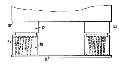
FIG. 1 illustrates a front plan view of the float/guide
member of the present invention as it appears when mounted between a
card edge connector and a mother printed circuit board, and showing a
second guide member mounted between a second card edge connector and
the mo~her printed circuit board at a spaced location from the first
float/guide member;
FIG. 2 is a perspective view of the float/guide member;
FIG. 3 is a front cross-sectional view of the float/guide
member taken along line 3-3 of FIG. 2;
FIG. 4 is a side cross-sectional view of the float/guide
member taken along line 4-4 of FIG. 3;
FIG. 5 ls a perspective view of a first alternative
embodiment for the float/guide member;
FIG. 6 i8 a top plan view of the float/guide member o~ FIG.
5;
FIG. 7 i8 a front cross-sectional view of the float/guide
member of FIG. 5, taken along line 7-7 of FIG. 6;
FIG. 8 i8 a side cross-sectional view of the float/guide
member of FIG. 5, taken along line 8-8 of FIG. 7; and
FIG. 9 is a side cross-sectional view of the float/guide
member of FIG. 5, taken along line 9-9 of FIG. 7.
~ ~30Q~02
DESCRIPTION OF THE PREFERRED EMBODIMENT
With reference to the drawings, and, in particular, with
reference to FIGS. 1-4, the preferred embodiment for a
float/guide member according to the principles of the present
invention is shown generally at 10. ~s illustrated in FIG.
l, the float/guide member 10 is intended to be inserted
between a card edge connector 12 and a mother printed circuit
board 14. The card edge connector, in turn, is electrically
associated with a daughter printed circuit board 16 oriented
vertically in a slot in the card edge connector.
As further shown in FIG. l, the card edge connector includes
a plurality of pin contacts 18 which, when the card edge
connetor i6 mounted on the float/guide member, extend
comple~ely through the float/guide member and pro~ect from
the bottom thereof. The ends of the pin contacts which
pro~ct from the bottom of the float/guide member extend into
the mother printed circuit board, being electrically
connected to the mother board by solder connections.
~9 iS most clearly shown in FIGS. 2-4, the float/guide member
lO comprises a body 20 fabricated of an insulative material,
preferably a glass-filled polyester. The body 20 is defined
by parallel front and rear walls 22 and 22' side walls 24,
top wall 26 and bottom wall 28, which ~ogether form a
generally rectangular configuration. Support members 30
pro~ect from the bottom wall 28, by means of which the body
may be supported upon the mother printed circuit board with
the bottom wall 28 slightly raised above the mother board as
_9_
~300702
shown in FIG. 1. The support members 30 provide a solder
wash standoff for the body when the projecting ends of the
contact members 18 are soldered to the mother printed circuit
board. The parallel front and rear sides of top wall 26 are
each provided with an upstanding side rail 31.
Top wall 26~ as illustrated in FIG, 2, is provided with a
plurality of openings 32. As best depicted in FIGS. 3 and 4,
openings 32 lead into contact receiving cavities 34 formed in
the body 20. Each of the cavities 34 extends vertically
through the body from the top wall 26 to the bottom wall 28,
tapering inwardly and downwardly from the top to the bottom
walls.
As prevlously discussed in con~unction with FIG. 1, the
float/guide member 10 is intended to be utilized in
con~unctlon with a card edge connector 12 and, preferably,
with a 2x6 0.100 inch pitch card edge connector ha~ing a
total of twelve pin contacts 18. In order for the pin
contacts 18 to be accommodated by the float/guide member, the
present invention contemplates lengthening and thinning the
associated card edge connector contacts. In particular, the
card edge lead is intended to be lengthened to around 0.75
inch, and the contact beam is thinned perpendicular to the
direction of float, the direction of float being in the
lateral direction parallel to the side rails 31.
With reference to FIG. l, it can be seen that the card edge
connector 12 is adapted to be inserted and snugly received
--10--
.
- ` ~3(~0;~
between the upstanding parallel rails 30 of the float/guide
member. The contact members 18 are intended to be press fit
into the float/guide member, each of the contacts extending
into a respective contact receiving cavity 34, whereupon each
of the contact members projects from a bottom opening 36 in
the bottom wall 28 of the float/guide member into the mother
printed circuit board for soldering thereto.
The pin contacts 18 are preferably rectangular, being
approximately 0.025 inch x 0.011 inch, the contact beam
having been reduced perpendicular to the direction of float.
It can be seen in FIGS. 2-4 that the openings 32 and the
contact receiving cavities 34 are circular in configuration
which, when receiving the rectangular pin contacts 18,
ensures washing. It is also evident from FIGS. 2-4, that the
openings 32 to the con~act receiving cavities are oversized
with respect to the slze of the contact member~, the openings
preerably being around 0.09 inch in diameter. Each of the
colltact receiving cavitles tapers inwardly and downwardly
from this 0.09 inch diameter opening to 0.028 inch in
diameter at approximately location 38, slightly above the
bottom opening 36. The contact receiving cavitie6 are a
constant 0.028 inch diameter from the location 38 to the
bottom openings 36.
Thu8, it can be seen that the contact member~ 18 are
relatively snugly received within the contact receiving
cavities from location 38 down to the bottom openings. From
~ 3~~'7~)2
location 38 upward, however, the enlarged area of the contact
receiving cavities allows the contact members to bend or
float laterally in their contact receiving cavities in the
lateral direction when the card edge connector is moved
laterally along the top wall 26 of the float/guide member.
The degree of float permitted by the float/guide member as
described is in the nature of +/-0.03 inch in the lateral
direction.
By allowing the card edge connector 12 to float laterally,
the daughter printed circuit board 16 associated with the
card edge connector is able to be properly aligned and
similarly mated with a fiecond card edge connector 50, as
shown in FIG. 1. The second card edge connector 50 may be
the same a8 or of a different pitch than the card edge
connector 12, the invention having particular application
where the second card edge connector 50 is a 2x120 0.050 inch
pitch card edge connector. Although FIG. 1 ~hows the second
card edge connector as being associated with the mother
printed circuit board 14, it should be understood that the
second card edge connector may be electrically connected to a
second different printed circuit bo~rd, thereby allowing a
single daughter board to be connected to two different
printed circuit boards.
The invention i9 characterized in that the thinning and
extending of the card edge connector contacts per~its lateral
movement of the card edge connector on its contacts without
-12
~3~7~2
any extraneous mechanical or solder connections. Press fit
of the contact ~embers in the float/guide member transfers
stress from the solder ~oint at the mother printed circuit
board and defines the moment of inertia for ~he contact
member. Stress on the thinned contact member is minimized by
means of the side rails limiting movement of the card edge
connector perpendicular to the transverse plane. Finally,
the maximum lateral float of the card edge connector is
defined by the contact receiving cavities of the float/guide
member, thereby limiting contact fatigue.
A first alternative embodiment for the float/guide member is
depicted in FIGS. 5-9. As shown therein, the float/guide
member 100 comprises a body 120, preferably fabricated Erom
glaAs-filled polyester. The body 120 is defined by front and
rear walls 122 and 122', side walls 124, top wall 126 and
bottom wall 128. Support members 130 pro~ect from the bottom
wall 128, the purpose of which was discussed in connection
with the embodiment of FIGS. 1-4. Additionally, a
cylindrical pro~ection 133 extends downwardly from the bottom
wall, providing a Means by which the float/guide member may
be secured to a printed circuit board or to an electrical
connector. The parallel front and rear sides of top wall 126
are each provided with an upstanding side rail 131.
Top wall 126, as best depicted in FIGS. 6 and 8, is provided
with a pair of parallel cavi~y receiving 810t8 129. Slots
129 are generally rectangular in cross-sectional
-13-
13~ )2
configuration, when viewed from above, being separated from
each other by a central web 133 of the body. The cavity
receiving slots 129 extend from the top wall vertically
downward through the body and terminate in a plurality of
circular contact receiving openings 132 which are shown in
FIGS. 6 and 7 as corresponding to the pin contact members 118
of a 2x6 card edge connector as was generally discussed in
connection with the preferred embodiment of FIGS. 1-4. Thus,
each of the slots 129 is adapted to receive an array of six
contact members of a 2x6 card edge connector.
Each of the contact receiving openings 132 tapers inwardly to
a second restricted contact receiving opening 137, whereupon
the second openings 137 taper outwardly to bottom openings
136 from which the pin contact members are adapted to
pro~ect. The inwardly and outwardly tapering arrangement may
be obtained by forming the second contact receiving openings
137 in the bottom wall and providing a 60 degree chamfer in
the bottom wall at the top and bottom of the openings. The
float/guide member 110 i8 intended to be utilized in the
manner discussed in connection with the float/guide member of
FIGS. 1-4.
In particular, the pin contact members 118 of a card edge
connector are intended to be inserted into the float/guide
member through the contact receiving slots 129, such that a
single contact member i9 received within each of the second
contact receiving openings 137. The upper and lower chamfer
-14-
~30~0;~
provided for each of the openings, as well as the slots 29present an enlarged area above and below the openings 137,
whereby the contact members are able to float laterally with
lateral movement of the associated card edge connector as was
discussed in connection with FIGS. 1-4.
Although the invention has been deYcribed in detail in
relation to a preferred and an alternative embodiment, it is
to be understood that various modifications, changes or
additions may be made to the invention as described herein by
one of ordinary skill in the art without departing from the
spirit and scope of the invention as defined in the appended
claims.
-15-