Note: Descriptions are shown in the official language in which they were submitted.
9~3V~)7~34
TITLE OF THE INVENTION
METHOD AND APPARATUS FOR TRANSFERRIN~ AND
PROCESSING TELEVISION SIGNAL
BACKGROUND OF TH~ INVENTION
Field of the Invention
The present invention relates to a method for
transferring a television signal ~uited for a high-
definition television signal.
Description of the Prior Art
It i~ well known that extremely broad
bandwidth i~ used for the high-definition televi~ion
signal (hereina~ter to be brie~ly called the HD video
signal~ as compared with the video signal for the
currerlt standard system (such as NTSC system). And for
recording the HD video signal, a digital recordit~g
system is preferred because it provides high quality of
reproduced image and causes, in dubbing, small
deterioration in the image quality.
However, the bandwidths and sampling
frequencies required for recording the HD video ~ignal
become 90 large, for exampleS as follows:
13~073~
video signal bandwidths Y 25.OMHz
Cw 12.5MHz
CN 12.~MHz
samp]ing frequencies Y 64.8MHz
CW 32.4M~z
CN 32.4MHz.
In case of quantization of eight bits for each
sample, the data rate of the digital data in ~uch
specification becomes 1037MB/s, which is extremely high
as compared with the case o~ the so-called 4-2-2 type of
digital VTR (sampling ~requency: 13.5MHz~ in the current
standard system (NTSC system). Fven in the case where
parallcl recording through four channel~ is practiced,
Por example, the data rate for each channel exceeds
250MHz/s. Thus, there was a problem that it was very
difficult to manufacture the magnetic head sy~tem
capable of such high speed recording and circuit devices
in use for the signal processing system to process the
signal to be supplied to such a magnetic head.
In view of the above defect, it is well-known
in the art that the high-speed data signals obtained by
sampling the broadband video sigDals such as the
afGrementioned high-resolution video signals are
converted into low-speed data signals. For example, as
~ 3 ~ 13~73~
. ~ . , .
shown in European Patent Application No. 0133026
published on February 13, 1985, it is disclosed that the
high-speed data signals corresponding to the displayed
picture are vertically divided into N sections wherein N
is an integer larger than 2 and the frequencies of the
divided data signals are frequency-converted by l/N and
transferred through N-channel transmission lines for
subsequent image processing.
~ owever, in case the data signals having the
above described specification of the high definition
video signal is recorded on magnetic tape by rotary
magnetic head, there still are difficulties in recording
band width, even if the frequency band of the data signal
is reduced by means of the aforementioned band reduction
manner.
OBJECTS OF THE INVENTION
. It is an object of the present invention to
provide an improved method and apparatus for transferring
a data signal having a high sampling frequency.
It is another ob;ect of the present invention
to provide new method and apparatus for transferring
digital data signals comprising component video signals,
wherein the digital data signals corresponding to the
displayed picture are divided into N sections ~or band
~_ ~3~
4 --
reduction.
It is a further object of the present invention
to provide method and apparatus for transferring and
processing digital data signals comprising component
video signals, wherein the component video signals are
each reduced in frequency band and the reduced component
video signals are sequentially interleaved with each
other.
BRIEF DESCRIPTION OF THE DRAWINGS
Figure 1 is a block circuit diagram of one
embodiment o~ the present invention.
Figure 2 illustrates the processing of a video
image by the apparatus of Figure 1.
Figure 3 shows in more detail the image area
dividing circuit of the appàratus of Figure 1.
Figures 4 and 5 are timing diagrams of the
operation of the circuit of Figure 3.
DBSCRIPTION OF THE PREFERRED EMBODIMENTS
An embodiment of the method for transferring a
television signal according to the present invention
applied to digital magnetic recording of the HD video
signal will be described below with reference to the
accompanying drawings.
~3~734
.
- 4a -
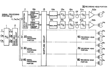
Referring to Fig. 1, a luminance component
signal Y and chrominance component signals Cw and CN are
supplied to an analog/digital converter 1. The frequency
bandwidths of the signals Y, Cw, and CN are,
~3~073~
for example, 25 MH2, 12.5 MHz, and 12.5 MHz,
respectively, as described above, which are sampled in
the analog/digital converter 1 at 64.8 MH2, 32.4 MHz,
and 32.4 MHz, respectively, where the quantization
number of each sample is 8 bits.
The signals y~ cw~ and CN which are digitized
in the analog/digital converter 1 are all supplied to an
image area dividing circuit (parallel dividing circuit)
2. This image area dividing circuit 2 i8 used for
dividing each of the ~ignals Y, Cw, and CN at equal
intervals in the horizontal direction on the television
screen as shown in Fig. 2. Each signal is divided into
four sections in the present embodiment. Corresponding
to the four outputs of the image area dividing cir-cuit
2, four signal processing portions 10, 20, 30, and 40
are provided in parallel, and the outputs of the image
area dividing circuit 2 are supplied to their respective
signal processing portions 10 - 40.
Since the signal processing portions 10 - 40
are all of the same structure, the first signal
processing portion 10 will only be described and
illustration and description of detailed structure of
the second to fourth signal processing portions 20 - 40
will be omitted here.
~3~0~3~
A signal processing portion 10 includes a data
di~tributing circuit 11, which distributes data of the
divided signals Y, Cw, and CN supplied from the image
area dividing circuit 2 to two error-correcting code
encoding circuit 12a and 12b. By this distribution,
there are formed two channels in the signal processing
portion 10. Output of both of the error-correcting
code encoding circuits 12a and 12b are supplied through
a shuffling circuit 13 common to all the signal
processing portion 10 - 40 to modulator circuits 14a and
14b and modulated therein, for example, by the scramble
NRZ ~ystem. The outputs of both of the modulators 14a
and 14b are converted into Rerial data in
parallel/serial converters 15a and 15b, respectively,
and ~upplied to electricity/light conversion elements
16a and 16b.
The optical outputs from th.e electricity/light
conversion elements 16a and 16b are supplied through
optical Pibers OF, respectively, to light/electricity
conversion elements 61a and 51b of a recording head
portion ~O to be converted therein back to electrical
signals. It shou.ld be noted here that interference by
mixing in of electrical noise specifically in the high
frequency domain is prevented by the use of the optical
13f)(~73~
tran~mission line. The outputs of the electricity/light
converting elements 51a and 51b are supplied through
amplifiers for recording 62a and 52b to recording
magnetic heads Hl and H2.
In like manner, the second, third, and fourth
signal processing portions 20, 30, and ~0 are connected
through optical fibers with the second, third, and
fourth recording head portions 60, 70, and 80, and the
recording head portions 60 - 80 include two recording
head9 H3~ H4; H5~ H6; and H7, Hg, respectively.
Although it i9 omitted in the illustration,
the four recording magnetic heads Hl, H2, H3, and H4 are
formed integral, and the four recording magnetic heads
Hs, ~l6, H7, and H8 are al~o formed integral, and these
two heat groups are attached to a rotating drum at an
angle of 180 . Since a magnetic tape (a metallic tape,
for example) is wrapped around the drum at Q wrapping
angle of approximately 330 , eight trucks are
simultaneously recorded by both of the head groups. And
it is arranged such that 16 -trucks correspond to one
field period.
The mechanism of the digital VTR of the
present embodiment is based upon the format type C and
the number of revolutions of the drum is arranged to be
~3~t~73~
7200 rpm. A one inch wide tape travels at the speed of
approximately 800 mm/s, and a 14-inch reel for three-
hour play for a YTR of the format type C can be used for
1.5 hour~ of recording or playback.
Now, the operations of the present embodiment
will be de~cribed with reference to Fig. 2.
By the parallel dividing process in the image
area dividing circuit 2, the ~ampling frequency of the
output therefrom i8 reduced to 16.2 MHz, 1/4 o~ the
previously mentioned 64.8 MHz. Details of the parallel
dividing process in the image area dividing circuit 2
will be described later. For the sake o~ simplicity, it
is assumed here that there are present eight pieces of
data on one scanning line of each of the divided screens
for the signals Y, Cw, and CN as shown in Fig. 2.
~ y the data di~tributing circuit 11, the data
Yl, Y3, Y6, and Y7 in odd-numbered places of the signal
Y are distributed to the error-correcting code encoding
circuit 12a of one of the channels ancl the data Y2, Y4,
Y6, and Y8 in the even-numbered places are distributed
to the error-correcting code encoding circuit 12b of the
other channel.
At this time, while the data for the signals
CW and CN are also to be distributed, since the
~3~ `73~
frequency bandwidth of the chrominance component signals
CW and CN is only 1~2 of that of the luminance component
signal Y, transmission of half the number of pieces of
these data suffice for the purpose. Therefore, in the
pre~ent embodiment~ Cwz~ Cw4. CW6~ and CW8~ an N2
CN4, CN6, and CN8, in the even-numbered places, for
example, are discarded. and CWl~ ~Nl~ CW5~ and CN5 are
distributed to one channel, and Cw3~ CN3, CW7, and CN7
are distributed to the other channel, and thus, the
luminance data at each sample point and the chrominance
data in its vicinity are adapted to be uniformly
digtributed.
The sampling frequency of the data from the
input to the data di~tributing circuit 11 to the output
of the modulators 14a and 14b i~ 16.2 MHz as previously
describedl and the circuit devices for processing
signals at ~uch a sampling frequency are easily obtained
by appropriation to this purpose of the circuit devices
for digital VTR of the current standard system (PAL or
NTSC system) or the like.
The data in each of the channels encoded to
Reed-Solomon product codes in the error-correcting code
encoding circuits 12a and 12b are converted by the
parallel/serial converters 15a and 15b into serial data
~`
13(~73~
at 129.6 MB/s of data rate. A magnetic head capable of
recording data at ~uch a data rate can be manu~actured
through the current magnetic head technique without much
difficulty.
According to the present embodiment, the
signal processing portions 10 - 40 supplied with the
outputs of the image area diYiding circuit 2 are each
provided with a data distributing circuit 11, etc.,
whereby each of the signal processing portions 10 - 40
and the recording he~d portions 50 - 8n Berially
connectecl thereto is arranged in two channels so that
totally eight channels of parallel transmission ~ystem
are provided. Therefore, the data rate tran~ferred
through each channel ha~ been enabled to be reduced and
recording (transfer) of dlgital data of the HD video
signal has been made ea~y-
The image area dividing circuit 2 in use foran embodiment of the present invention will be described
below with reference to Fig. 3. The circuit of Fig. 3
is that iB ~eparately provided for each of the digit~l
luminance signal and the digital chrominance signals C~
and CN.
Eight-bit parallel data ~B, D in Fig. 4) of
the digital video signal (the luminance component signal
L30(~ 34
Y or digital chrominance component ~ignal Cw or CN) from
the analog/digital converter 1 of the digital VT~ of
Fig. 1 is supplied to Q shi.ft regi~ter 260. Since the
digital video signal for one screen i9 made up of 2000
samples in the horizontal direction and 1050 lines in
the vertical direction, and this digital.video signal is
equally divided into ~our sections for each line, 500
samples each thereof will be ~equentially called the
first - fourth ~eries, ~ - ~ . A sample clock CKl (C
in Fig. 4) at the frequency of 64.~ MHz (the period is
represented by T) i3 supplied to the shift re~ister 260
whereby the digital video signal is shifted. Four-bit
output~ Q4 - Ql of the shift register 260 are ~upplied,
respectively, to ~our re~isters 201 - 204, each thereof`
being provided with an input enable terminal, and
latchcd therein by a load pul~e LDl tE in Fig. 4),
having 16.2 MHz of frequency and becoming low every 4-T
period for the duration of 1 T, so as to be output in
parallel. The clock CKl is also supplied to these
register~ 201 - 204. And, each of the output data
series DlA - D4A tF - I in Fig. 4) of the registers 201
- 2Q4 are ~upplied to register~ 211, 21Z; 221, 222; 231,
232; and 241, 242, each thereof being provided with
output enable terminals, and latched by a olock CKll (J
-
13QC~34
in Fig. 4) at the frequency of 16.2 MHz.
To the output enable terminals of the
registers 211, 221, 231, and 241 i~ ~upplied the
inverted pulse by an inverter 263 of the line
identification pulse LNID (A in Fig. 4) which is
alternately brought high and low at intervals of one
line, while the line identification pulse LNID as it is
is supplied to the output enable terminals of the
registers 212, 222, 232, and 242. Hence, the registers
211, 221, 231, and 241 and the registers 212, 222, 232,
and 242 output their data alternately for sach line
period. That is, when the line identi~ication pulse
LNID ls at the high level, output dat~ series DllA,
D21A, D31A, and D41A (K - N in Fig. 4) ~rom the
registers 211, 221, 231, and 241 are supplle~ to
memories MllA, M21A, M31A, and M41A, respectively, and
when the line identification pulse LNID is at the low
level, output data serie~ D12A, D22A, D32A, and D42A
~rom the registers 212, 222, 232, and 242 are supplied
to memories M12A, M22A, M32A, and M42A, respectively.
A write enable pulse WE (O in Fig. 4)
frequency thereof being 16~2 MHz and duty ratio thereof
being 50% is ~upplied to OR gates 2~1 and 262. Further,
the line identific~tion pulse LNID i~ supplied to the OR
~L3~)73~
gate 261 and the inverted pulse by the inverter 263 of
the liDe identification pulse LNID is supplied to the OR
gate 262. And, output of the OR gate 261 is supplied to
the memorie~ MllA, M21A, M31A, and M~lA as a write
enable pulse, and output of the OR gate 262 is ~upplied
to the memories M12A, M22A, M32A, and M42A as a write
enable pul~e. Hence, when the line identification pulse
LNID is at the high level, the memories MllA, ~21A,
M31A, and M41A are brought into a write state, while the
memories M12A, M22A, M32A, and M42A are brought into a
read state. And, when the line identification pulse
LNID is at the low level, the memories MllA, M21A, M31A,
and M41A are brought into a read state, while the
memories M12A, M22A, M32A, and M42A are brought into a
write state. These memories meet the purpose if
provided with lk x R bits or so of capacity.
The clock CK 11 i~ supplied to an addres~
counter 269, and a write address therefrom i8 supplied
to each of the memories M12A, M22A, M32A, and M42A
through a multiplexer 266 which is controlled for
~witching by the inverted pulse by the inverter 263 of
the line identification pulse. And, the write address
from the address counter 264 i~ supplied to each of the
memories MllA, M21A, M31A, and M41A through a
13(~(~739~
multiplexer 267 which is controlled for switching by the
inverted pulse by the inverter 263 of the line
identification pulse. Further, the write addre~s from
the addre3s counter 26~ is supplied to a ROM 265 to be
subjected therein to later described address conversion,
and the thus obtained read addres~ is supplied through
the multiplexer 266 to each of the memories M12A, M22A,
M32A, and M4ZA. And, the read address from the ROM 265
is supplied through the multiplexer 267 to each of the
memories MllA, M21A, M31A, and M41A.
The write addre~s of each memory, as indicated
by P in Fig. 4, is a regular address 3equentially
incremented a~ 0, 1, 2, 3, .--- . And, the memory MllA
i8 written in, for example, with the data of the first
series ~ at the address 2 - 126, with the data of the
~econd serie~ ~ at the Qddress 127-261, with the data
of the third series ~ at the address 252 - 376, and
with the data of the fourth series ~ at the address
377-501. From the temporal viewpoint, these data are of
every fourth sample.
When the line identification pulse LNID (W in
Fig. 5) is at the low level, the data ~eries read out
from the memories MllA, M21A, M31A, and M41A are
supplied, respectively, to registers 213, 223, 233, and
14
~L3~373~
243, each thereof being provided with an output enable
terminal, and latched by the clock CKll (A in Fig. 6).
And, when the line identification pulse LNID is at the
high level, the data read out from the memories M12A,
M22A, M32A, and M42A are supplied, respectively, to
registers 214, 224, 234, and Z44, each thereof being
provided with an output enable terminal, and latched by
the clock CKll. As described above, the read address of
each memory is obtained by address conversion in the ROM
265, and the ~ame is arranged in the order of 0, 125,
250, 376, 1, 126, 251, 376, .-.- , with two pieces each
of the address ~or overlap portions at the front ancl the
rear and the addres~ for the first series ~ , second
serie~ ~ , third series ~ , and the fourth series ~ in
between.
To the output enable terminals of the
registers 213, 223, 233, and 243, the line
identification pulse LNID (W in Fig. 5) alternately
brought high and low at intervals of one line is
~upplied, and to the output enable terminal of the
registers 214, 224, 234, and 244, the inverted pulse by
the inverter 263 of the line identification pulse LNID
is ~upplied. Therefore, the regi~ters 211, 221, 231,
and 241 and the registers 212, 222, 232, and 242 make
-` ~3~
output operation~ alternately for each line period.
Data series D13A ~C in Fig. 5) and D14A from
the register~ 213 and 214 are supplied to registers 215,
225, 235, and 245, each thereof being provided with
input and output enable terminals. Data series D23A (D
in Fig. 6~ and D24A from tbe registers 223 and 224 are
supplied to registers 216, 22~, 236, and 246, each
thereof bein provided with input and output enable
terminals. Data series D33A ~E in Fig. 5) and D34A from
the registers 233 and 234 are supplied to registers 217,
227, 237, and 247, each thereof being provided with
input and output enable terminals. And, data series
D43A ~F in Fig. 6) and D44A from the registers 243 and
244 are supplied to registers 218, 228, 238, and 248,
each thereof being provided with input and output enable
terminals. Incidentally, Pl - P8 in Fig. 5 indicate
invalid data.
While the clock CK 11 is supplied to the
registers 215 - 218, 226 - 228, 235 - 238, and 245 -
248, the write address from the write address counter
Z64 i8 subjected to address conversion by a ROM 268 and
4-bit control signal6 GlA - G4A (G, ~, I, and J in Fig.
5) from the ROM 268 are supplied to their input enable
terminals and output enable terminals, and thereby,
16
iL3(;~(~73~
inputs thereto and outputs therefrom are controlled.
___ _
These control signals GlA - G4A have 4.05 MHz of
frequency and are held at the low level for a 4-T period
at intervals of a 16-T period, and their phases are
shifted by 4T from one another.
The output data serie~ D13A, D23A, D33A, and
D43A from the registers 213, 223, 233, and 243 are
latched, respectively, by the registers 215 - 218 ~hen
the control signal GlA is at the low level, by the
registers 225 - 228 when the control signal G2A is at
the low level, by the registers 235 - 238 when the
control signal G3~ is at the low level, and by the
registers 245 - 248 when the control ~i~nal G4A i~ at
the low level.
As apparent from C - F in Fig. 5, the
registers 215 - 218 only latch the data of the first
~erles ~ , the regist0rs Z26 - 228 only latch the data
of the second serie~ ~ , the registers 235 - 238 only
latch the data of the third series ~ , and the registers
245 - 248 only latch the data of the forth series ~ ,
each data thereof including overlap portions Rt the
front and rear.
The data seri0~ of the -first series ~ latched
by the registers 215 - 218 is ~equentially supplied to a
1`7
.
~3~ 3~
programmable shift register 251 in the order of the
control signals GlA - G4A. The data series of the
second series ~ latched by the registers 225 - 228 is
sequentially supplied to a programmable shift register
252 in the order of the control signals GlA - G4A. The
data series of the third series ~ latched by the
registers 235 - 238 i~ sequentially supplied to a
programmable shift register 253 in the order of the
control signals GlA - G4A. And, the data series of the
fourth series ~ latched by the r~gisters 245 - 248 i8
sequentially supplied to a programmable ~hift register
254 in the order o~ the control ~ignals GlA ~ G4A.
Each of the data ~eries RlA - R4A supplied to
the programDIable shift registers 251 - 254 are indicated
by K - N in Fig. 5, which are not in pbase one another.
Relative values o~ shi~t amounts SlA, S2A, S3A, and S4A
of these programmable shif`t registers 261 - 254 are set
to a 4-, 3-, 2-, and l-sample period, respectively.
These programmable shift registers 251 - 254 are
supplied with the clock GKll as the shift pul~e.
Thus, from these programmable shift registers
251 - 254 are output diital signals DATA ~1 - DATA #4
(O - R and S - V in ~ig. 5), which are the digital video
signals for four screens, namely, the divided screen of
18
-
~L3C~73~
the original screen into four sections in the horizontal
direction being expanded to the size of the original
screen and provided with overlap portions at both sides
thereo~.
The four digital signals DATA #1 - DATA #4 are
supplied to the data di~tributing circuit 11 of the
signal processing porticns 10 - 40, respectively.
19
--