Note: Descriptions are shown in the official language in which they were submitted.
~3(~9Z3
lA 310/700
TAH'cp
12/5/86
1796N
CO~PARATIVE COLORIMETER
This invention relates to a comparative
colorimeter, and more specifically to an instrument
which simultaneously compares the color (i.e.,
optical) densities of two liquid samples and
designates the degree of difference.
A colorimeter is useful for conducting:
(a) medical diagnostic tests based on enzyme
immuno assays (EIA), e.g., the test for
Leutenizing Hormone as an indication of
ovulation in humans:
(b) medical diagnostic tests based on Enzyme
.ultiplied Immuno assay Technique (EMIT),
e.g., tests for drugs of abuse such as
barbituates:
(c) veterinary diagnostic tests based on either
~a) or (b), e.g., progesterone level in
dairy cows;
13~ 123
lA 310/700
TAH'cp
12/5/86
1796N
(d) environmental tests based on either (a) or
(b), e.g., residual Chlorodane levels after
extermination around residences; and
(e) determination of the concentration of
certain chemicals based on absorption of a
given
wavelength of light, e.g., concentration of
the herbicide DynasebTM.
In the above-identified tests, it is generally
not the absolute value of optical density of a
solution which is of interest, but rather a
comparison of a sample solution with a standard
solution. Further, while all of these tests can be
satisfactorily performed in the laboratory using a
standard off-the-shelf spectrophotometric
instrument, such instruments are delicate and
expensive and are not adapted for use in the field.
For example, a colorimeter is useful in the field to
determine whether the residual level of a pesticide
applied to a crop has declined sufficiently to allow
safe entry of personnel into the field for
harvesting operations. A known colorimeter used in
the field performs separate quantitative
determinations of the optical densities of a sample
1 25 solution and a standard solution. ~he human
operator then computes the difference between the
; quantitative determinations. This device has
13()~9Z3
lA 31~)/700
TAH ' cp
12/5/8 6
1 796N
several disadvantages. First, since the operator is
generally interested in only the relative difference
between the sample and standard, it is a waste of
effort to make a quantitative determination for each
of the sample and standard. Further, since the
quantitative determinations of the sample and
standard are made at different times, there exists a
large potential for error if either of the solutions
changes in optical density with respect to time or
temperature.
It is an object of the present invention to
provide a relatively low-cost comparative
colorimeter for use in the field for comparing the
optical densities of two solutions and indicating
the relative degree of difference.
It is another object of this invention to
provide a comparative colorimeter for simultaneously
evaluating the optical densities of sample and
standard solutions prepared at the same time in
order to eliminate any error caused by changes in
the optical densities of the sample and standard
with respect to time.
It is a further object of this invention to
provide an optical subsystem for a colorimeter which
reduces the error caused by defects in the sample
tube such as scratches, irregularities or striations
in the tube wall, and lack of concentricity.
13~(;1923
lA 310/7D0
TAH'cp
12/5/86
1796N
It is still another object of this invention to
provide an electronic subsystem, including low-cost
digital integrated circuits, for quantifying the
difference between the optical densities of the
sample and standard solutions.
It is a still further object of this invention
to provide a correction circuit to eompensate for
variations in the threshold voltage of the digital
IC components with respect to batch, time,
temperature, and supply voltage.
It is still another object of this invention to
provide a correction circuit to compensate for
differences in the optical paths of the sample and
standard solutions.
The apparatus of this invention provides a means
for simultaneously comparing the optical densities
of two solutions and generating an output indicative
of the degree of difference. The apparatus includes
two major subsystems, optical and electronic.
The optical subsystem is designed to provide
identical light paths through two liquid samples
disposed in optically transparent sample tubes and
to minimize the effect which imperfect sample tubes
have on the measurement. The optical subsyste~
includes a light source means for transmitting a
pair of substantially equal light beams, one to each
13~ 9~3
lA 310/700
TAH ' cp
1 2/S/8 6
1796N
_5_
of a pair of photodetectors. Each of the two liquid
samples are simultaneously and identically
positioned between the light source means and an
associated photodetector. The photodetectors
generate a pair of optical density output signals
representative of the amounts of light passing
through the samples and reaching the
photodetectors. The optical system is designed to
spread the light over a substantial portion of each
sample tube to minimize the effect of defects in the
tubes.
In one embodiment of the optical system of this
invention, a collimating lens is positioned between
the sample ~ube and light source and spaced slightly
closer to the light source than the focal point of
the lens so that the lens transmits a slightly
divergent beam of light to the tube. The tube is
spaced with respect to the lens so that the outer
diameter of the divergent beam at the center plane
of the tube is substantially equal to the inner
diameter of the tube. The sample tube acts as a
cylinder lens to focus the beam at a vertical focal
line, and the photodetector is spaced slightly ahead
of the focal line so that the beam strikes a
substantial portion of the photodetector. The
photodetector output is substantially independent of
defects in the sample tube.
13(~ 9;2~
lA 310/700
TAH'cp
12/5/86
1796N
--6--
Preferably, the optical system further includes
a combination filter/diffuser positioned between the
sample tube and photodetector. The filter/diffuser
includes a filter for selecting a predetermined
wavelength of light and a light diffusing layer for
averaging the effect of individual defects in the
sample tube so that the photodetector output is less
affected by such defects. Preferably, the light
diffusing layer is disposed over the surface of the
filter adjacent the photodetector. In a further
preferred embodiment, a plurality of such
combination filter/diffusers are connected in serial
arrangement and the photodetector is positioned
adj~ining a light diffusing layer at one end of the
series.
In a second embodiment of the optical system of
this invention, a first lens set is positioned
between the sample tube and light source. The first
lens set includes a first collimating lens disposed
- 20 adjacent the light source and having a focal point
at the light source, and a first converging lens
disposed adjacent the sample tube and having a focal
point at the center of the sample tube. A second
lens set is positioned between the sample tube and
photodetector. The second lens set includes a
second collimating lens disposed adjacent the sample
tube and having a focal point at the center of the
~3(~1~923
lA 310/700
TAH'cp
12/5/86
1796N
--7--
tube, and a second converging lens disposed adjacent
the photodetector and having a focal point at the
photodetector. Because in this second embodiment
the light rays pass perpendicularly through the tube
and the tube has no focusing effect, refraction is
reduced and irregularities in the tube do not affect
the focus point. Thus, the accuracy of this second
embodiment is less dependent on the spacing between
the lenses and tube than that of the first
embodiment. A filter may be positioned between the
two lenses of the second lens set, and because the
light passes through the filter in parallel rays,
there is minimal reflection at the filter surface
and thus minimal light loss~
The electronic subsystem of this invention
provides a high level of accuracy and stability
despite the stringent cost limitations imposed by
the intended application. In particular, the
circuit utilizes low-cost digital components to
achieve a quantified output indicative of the degree
of difference in optical densities of the two
samples. A correction circuit is provided to
compensate for variations in the threshold voltage
of the digital IC components and to compensate for
differences in the optical paths of the two samples.
The electronic subsystem includes a differential
circuit means for generating a difference signal
13U(~923
lA 310/700
TAH'cp
12/5/86
1796N
representative of the difference between the optical
density output signals of the photodetectors. The
system further includes a comparative circuit
including means for comparing the difference signal
to a plurality of predetermined references and a
means for indicating the relative value of said
difference signal with respect to said predetermined
references.
In a preferred embodiment, the current outputs
of a pair of photodiod~s are logarithmically
converted to voltage signals and the resultant
voltage signals are differentially amplified to
produce a difference signal. The difference signal
is sent to a resistive chain including a plurality
of nodes, each node having a different predetermined
reference voltage. A plurality of digital gate
means each having the same threshhold voltage are
each connected to one of said nodes. The outputs of
the gate means activate a plurality of indicator
means to indicate the relative value of the
difference signal with respect to the predetermined
reference voltages.
In addition, a correction circuit is provided
for referencing the difference signal to the
, 25 threshold voltage of the gate means. The correction
circuit includes an additional gate means from the
same batch used in the comparative circuit. The
~3VC~9~3
lA 310/700
TAH'cp
12/5/86
1796N
_g_
output of the correction circuit, which is
referenced to the threshold voltage of the gate
means, is a~plied to the comparative circuit so that
the difference signal is referenced to the threshold
voltage. Further, the correction circuit includes a
zeroing mechanism to compensate for differences in
the light paths of the two sample solutions.
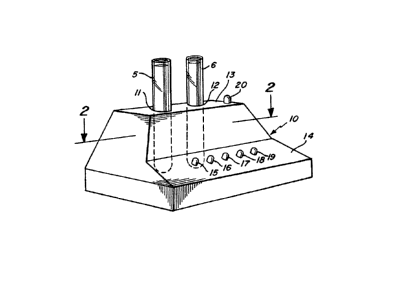
Fig. 1 is a perspective view of the comparative
colorimeter of this invention.
Fig. 2 is an illustrative top view of a first
embodiment of the optical subsystem of this
invention.
Fig. 2A is an illustrative top view of the
filter/diffuser and photodetector combination of
this invention.
Fig. 3 is an illustrative top view of a second
embodiment of the optical subsystem of this
invention.
Fig. 4 is an illustrative top view of a prior
art optical system.
Fig. 5 is a schematic diagram showing the
circuit means for logarithmically converting the
current outputs of the photodiodes to voltage
signals and means for differentially amplifying the
resultant voltage signals to produce a difference
signal.
:130l~9~3
lA 310/700
TAH'cp
12/5/86
1796~
--10--
Fig. 6A is a schematic diagram of three major
portions of the electronic subsystem of this
invention, including the log conversion and
differential amplifier circuit, the correction
c circuit, and the comparative circuit.
Fig. 6B is a schematic diagram of the supply
regulator circuit and an incandescent light source.
Fig. 6C is a schematic diagram of an alternative
light source comprising two LED's.
Fig. 7 is an illustration of the transfer
characteristic for an IC digital hex inverter.
Fig. 1 is a perspective view of the comparative
colorimeter of the present invention. A housing 10
contains the optical and electronic subsystems of
this invention. A pair of sample tube holders 11,
12 consist of tubular bores disposed vertically in
the housing and having closed lower ends and open
upper ends in the top wall 13 of the housing. The
holders snugly engage two cylindrical sample tubes
5, 6 which contain the sample and standard solutions
respectively. A row of five indicator lights 15,
16, 17, 18, 19 is provided on the front wall 14 of
the housing. An on-off button 20 is provided on top
wall 13 of the housing. The housing is made of a
nonbreakable plastic such a~ acrylonitrile-butadiene-
styrene polymer. The device shown in Fig. 1 is
3 3V~923
lA 310/700
TAH'cp
12/5/86
1796N
--11--
compact and portable, being 5" (127 mm) wide, 2.5"
(64 mm) high, 3" (76 mm) deep, and weighing about
200 grams. Typically, sample tubes 5, 6 are made of
polystyrene and have outer dimensions of 12 mm in
diameter and 75 mm in length, and an inner diameter
of 9 mm.
The comparative colorimeter of this invention
consists of two major subsystems, optical and
electronic. The important features of the optical
subsystem include:
(a) it must provide equal light paths through
both of the sample tubes; to the extent
that the light paths are not identical,
then the ratio of light
going through them must be constant
despite: the buildup of dirt and
contamination; thermal effects; warping or
flexing of the printed circuit board or
other structural members; mechanical shock
- and abuse and aging of various components,
e.g., light bulb and filters;
(b) it must provide adequate light intensity at
the photodiodes under all operating
conditions;
2~ (c) it must minimize the effects of stray or
ambient light; and
~3()~923
lA 310/700
TAH'cp
12/5/86
1796N
-12-
(d) it must minimize the effect of imperfect
sample tubes.
In a laboratory spectrophotometric instrument,
the samples are held in square cuvettes with ground
and polished plane sides so that the sample
container contributes little or no uncertainty to
the measurement. In the field it is desirable to
use inexpensive and disposable cylindrical plastic
; test tubes. However, these test tubes may
contribute significantly to the uncertainty of the
measurement. A typical plastic tube suffers three
principal defects:
(a) it may be scratched to a greater or lesser
degree, depending on the care with which it
is handled; these scratches tend to scatter
and diffuse light, making the light path
indeterminate;
(b) it may contain striations or irregularities
in the wall of the tube, which will refract
2C light in an indeterminate way and
(c) the tube's exterior and interior may not be
concentric, so that the actual path length
and direction of a light ray passing
through the sample depends on the
l 25 orientation of the tube.
The degree to which these imperfections
contribute uncertainty is highly dependent on the
details of the optical design.
130~9~3
lA 310/700
TAH'cp
12/5/86
1796N
In the prior art design shown in Fig. 4, a
narrowly collimated or focused beam of light from a
lamp 200 passes through a sample tube 201 and then
through a lens 202 which focuses the beam on a
photodetector 203 which is sensitive to a
predetermined wavelength. A screen 205 having an
aperture 206 is disposed between the lamp and tube
to prevent stray light from reaching the
photodetector. A filter 204 is disposed between the
lC lens and photodetector for selecting light of a
predetermined wavelength. In this prior art design,
it is desirable to pass a very narrow beam of light
through the center of the tube only so that the
light beam passes through a sample area having a
roughly uniform thickness. This is required where a
quantitative determination of absorbance is being
made and it is necessary to know the dimensions of
the sample through which the beam passes. However,
individual defects in the area of the sample tube
through which the beam passes have a significant
effect on the photodetector output.
All of the above-mentioned defects in the
plastic sample tubes affect the measurement results
of this prior art design very severely. Typically,
a measurement in absorbance may contain an error of
.05 tG .1 as a result of tube defects alone. The
amount of error is highly dependent on the
individual tube under test and its orientation.
130Q923
lA 310/700
TAH'cp
12/5/86
1796N
-14-
Two designs have been found to be highly
effective at minimizing the errors caused by sample
tube defects. These designs are shown in Figs. 2
and 3.
A first embodiment of the optical subsystem is
shown in Fig. 2. A pair of photodetectors 30, 31
are positioned at opposite ends of an axial line. A
light source means 32, such an incandescent lamp, is
centered at the midpoint of the axial line. A first
sample tube 5 and a second sample tube 6 are
identically positioned on the axial line on opposite
sides of the lamp, between the lamp and an
associated photodetector. A collimating lens
33A(33B1 and a screen 34A(34B) having an aperture
35A(35B) are identically positioned on either side
of the lamp between the associated sample tube 5(6)
and lamp 32. A filter/diffuser 36A(36B) is
positioned between the associated sample tu~e 5(6)
and associated photodetector 30(31).
The object of this first design is to spread the
illumination over substantially the entire width of
the sample tube so that the net light transmitted to
the photodetector is averaged over many scratches
and defects and is minimally dependent on the lack
of concentricity of the inner diameter and outer
diameter of the tube. While the operation of the
optical system with respect to sample tube 5 is
13~)C19Z3
lA 310/700
TAH'cp
12/5/86
1796N
described herein, the operation with respect to
sample tube 6 is identical.
The collimating lens 33A is positioned between
the sample tube 5 and light source 32 and spaced
S slightly closer to the light source than the focal
point of the lens so that the lens transmits a
slightly divergent beam to the sample tube. The
screen 34A prevents stray light beams from reaching
the photodetector 30. Further, the height of the
aperture 35A is restricted to prevent light from
hitting the meniscus of the liquid sample in the
tube or the bottom of the tube and reflecting into
the photodetector. The sample tube 5 is spaced with
respect to the lens 33A such that the outer diameter
of the divergent beam at the center plane of the
tube is equal to or slightly less than the inner
diameter d of the tube. The sample tube acts as a
cylinder lens to focus the beam at a vertical focal
line and the photodetector is spaced slightly ahead
of the focal line so that the beam strikes a large
area of the photodetector. This insures a
, photodetector signal of large amplitude and averaged
j value.
The combination filter/diffuser 36A
disposed between the sample tube ~ and photodetector
30 consists of a filter glass 39 for selecting a
predetermined wavelength of light and a diffusive
~30C~923
lA 310/700
TAH'cp
12/5/86
1796N
-16-
sheet or film 40 covering the surface of the filter
glass adjacent the photodetector. For example, film
40 may be MylarTM film frosted on both sides and
about .006" (.15 mm) thick. Because scratches and
defects in the sample tube cause light to bounce in
a random manner, the diffusive sheet 40 is provided
to produce an averaging effect so that the
photodetector output is less dependent on defects in
the sample tube. Preferably, the photodetector 30
0 i8 sensitive to the same predetermined wavelength as
the filter glass 39.
A preferred embodiment of the filter/diffuser is
shown in Fig. 2A. Two pieces of filter qlass 41, 43
and two sheets of diffusive film 42, 44 are
san2wiched together and disposed adjoining a
photodetector 45. Diffusive sheet 42 is sandwiched
between filter glasses 41 and 43, and diffusive
sheet 44 is sandwiched hetween filter glass 43 and
photodetector 45. This filter/diffuser is preferred
because the addition of a second diffusive film
separated from the first aids in a more uniform
diffusion of the light. The use of a second filter
glass is necessary in most cases in order to limit
the bandwidth of the light transmitted. Further,
adjoining the photodetector 45 to diffusive layer 44
eliminates light loss and increases the amplitude of
the photodetector output.
13~9~:3
lA 310/700
TAH'cp
12/5/86
1796N
-17-
A second embodiment of the optical subsystem of
this invention is shown in Fig. 3. Again, the
design spreads the light beam over a large area of
possible defects in the tube. A first lens set 50A
includes a pair of diametrically opposed lenses 51A,
52A positioned on an axial line between the sample
tube 5 and light source 32. Collimating lens 51A is
disposed adjacent the light source and has a focal
point at the light source. Converging lens 52A i6
disposed adjacent the sample tube and has a focal
point at the center of the sample tube. A second
lens set 54A includes a second pair of diametrically
opposed lenses 55A, 56A positioned on the axial line
between the sample tube 5 and photodetector 30.
Collimating lens 55A is disposed adjacent the sample
tube and has a focal point at the center of the
sample tube and converging lens 56A is disposed
adjacent the photodetector and has a focal point at
the photodetector.
In the second embodiment, because the light rays
pass perpendicularly through the sample tube and the
tube has no focusing effect, irregularities of the
tube do not affect the focal point. Thus, the space
between the lenses and sample tube is less critical
in this design~ Furthermore, in the second
embodiment a filter 57A can be placed between the
two lenses 55A, 56A of the second lens so that the
light
130~9~3
lA 310/700
TAH'cp
12/5/86
1796N
-18-
rays pass through the filter as parallel rays. This
minimizes refractions at the surface of the filter
and thus reduces light loss.
In Fig. 3, the first and second lens sets 50B
and 54B between the lamp 32, sample tube 6 and
photodetector 31, are identical to those of 50A and
54A previously described.
To evaluate the effectiveness of the designs
shown in Figs. 2 and 3, in comparison with the prior
art design of Fig, 4, a series of measurements was
taken with one particular sample tube filled with a
sample solution. Eight different orientations of
the tube were tried for each design to find the
range of readings resulting from the one sample and
tube. The resulting inaccuracy can be expressed as
an error in absorbance as follows:
~ A = logl(Imax - Imin)/2Iav]
where ImaX = maximum light intensity
~o resulting from the series of readings for a given
sample, tube and optical design;
Imi" = minimum light intensity resulting
from the series of readings for a given sample, tube
and optical design and
~3~1~9;~3
lA 310/700
TAH'cp
12/5/86
1796N
--19--
IaV = average light intensity resulting
from the series of readings for a given sample, tube
and optical design.
Design 1 was that shown in Fig. 2 with lens 33A
having a diameter of 5/16" and a focal length of
3/8". Lens 33A was spaced .27" from lamp 32, screen
34A, having an aperture .125" x .275", was spaced
.40" from lens 33A, tube 5 was spaced .35" from
i screen 34A, and photodiode 30 was spaced .65" from
tube 5 (all distances are from center point of
element). The filter/diffuser used was that shown
in Fig. 2A wherein 41 was a 2 mm thick filter glass,
model GG-435 by Schott, imported by ESCO Products,
Inc. of Oak ~idge, New Jersey, and 43 was a 4.0 mm
thick filter glass, model 5-58 by Corning Glass
Works of Corning, New York. Each filter glass had a
diameter of 5/16". The diffuser sheets 42 and 44
were MylarTM film, each .006n thick and frosted on
both sides. The photodiode was adjoining sheet 44.
Design 2 was that shown in Fig. 3 with lenses
51A, 52A, 55A and 56A each having a diameter of 3/8"
and a focal length of 1/2". The first lens set was
spaced .5" from lamp 32, tube 5 was spaced .5" from
the first lens set, lens 55A
was spaced .5" from tube 5, lens 56A was spaced .25"
from lens 55A, and photodiode 30 was spaced .5" from
13(~C~923
- lA 310/700
TAH'cp
12/5/86
1796N
-20-
lens 56A (all distances are from center point of
element). Two filter glasses, the same as 41 and 43
described in design 1 (but without diffusive sheets
42 and 44) were used. In design 2, the distance
between the lenses and sample tube could be changed
up to 1/16" (1.6 mm) without changing the
photodetector reading significantly. In comparison,
in design 1, the sample tube had to be spaced within
5/1000" (.13 mm) with respect to the lens and with
respect to the axial line extending between the lamp
and photodetector to insure a consistent
photodetector reading
The prior art design was that shown in ~ig. 4
with lens 202 having a diameter of 5/16" and a focal
length of 3/8". Screen 205 had an aperture 206 of
1/10" in height. The same two filter glasses
described for design 2 were used.
In all designs an incandescent lamp was used,
model 158X sold by Gilway of Woburn, Massachusetts.
The sample tube was made of polystrene having a
length of 12 mm, an outer diameter of 75 mm, and an
inner diameter of 9 mm. The photodiode was model
S-1133 sold by Hamamatsu of San Jose, California.
The following values of aA were obtained for
the prior art design and designs 1 and 2 of the
present invention:
13~ 923
lA 310/700
TAH'cp
12/5/86
1796N
-21-
PRIOR ART DESIGN ~ A = .05
DESIGN 1 ~ A = .01
DESIGN 2 ~A = .004
Thus, it has been shown that both design 1 and
design 2 of this invention give substantially better
results than the
prior art design. ~hile it would appear that design
2 is preferable over design 1, other factors such as
cost, size, complexity and the required accuracy of
construction mitigate in favor of design 1.
The electronic subsystem of the present
invention, as shown in Fig. 6A, performs the
following functions:
(a) the current outputs IDl and ID2 f the
two photodiodes PDl and PD2 are
logarithmically converted to voltage
signals;
(b) the two voltage signals are differentially
amplified at A3 to produce a difference
signal Eo
(c) the difference signal Eo is compared to a
plurality of predetermined reference
voltages with a series of voltage
comparators, consisting of digital gate
means Gl-G5 and resistive chain R12-R17
13V~1923
lA 310/700
TAH'cp
12/5/86
1796N
-22-
(d) the digital gate means drive a plurality
of indicator LEDs l-S (corresponding to
indicator lights 15-19 in Pig. 1) to
indicate the relative value of the
difference signal with respect to the
reference voltages; and
(e) a correction circuit is provided so that
the difference signal Eo is referenced to
the threshold voltage E~ of the digital
gate means.
The indicator lights or LEDs 15-19 of Fig. 1,
which correspond to LED's 1-5 of Fig. 6A
respectively, indicate the degree of difference in
optical density between the samples in the tubes.
If the sample and standard solutions have equal
optical densities, then a middle green LED 17 turns
on to indicate the same. If the solution of tube 5
has a lesser optical density than the solution of
tube 6, when the difference exceeds a first
pre~etermined level the comparator will trigger a
right center red LED 18 and simultaneously
extinguish the green LED, and if the difference
exceeds a larger second predetermined level, then a
right red LED 19 will light. At no time is more
than one indicator LED on~ If the solution of tube
5 has a greater optical density than the solution of
tube 6, then the left center red LED 16 and left red
i30C'9;~:3
lA 310/700
TAH'cp
12/5/86
1796N
-23-
LED 15 will light in the same manner as described
for those to the right of center. A typical
configuration is for the right center LE~ 18 (and
left center LED 16) to come on at ~A = .03 O.D.
(difference in absorbance between the tubes is .03),
and the right LED 19 (and left LED 15) to comes on
at ~ A = 0.1 O.D.
The operating voltage VREG for the lamp and
the electronic subsystem is stabilized at 2.000
volts by the supply regulator circuit shown in Pig.
6B. The circuit includes amplifier A4, capacitors
Cl, C2, C7, C8, resistors R1, R2, R3 (variable), R4,
R7, R22, R23, transistors Ql, Q2, battery V+, and
internal regulator VREF. A range of battery
voltages V+ from 3.0 to 2.1 volts can be
accommodated without degrading performance. Lamp
life is extended substantially by operating the lamp
32 at a constant 2.0 volts.
The regulator circuit is built around one
section of a amplifier A4 specifically intended for
voltage regulation. A4 in this preferred embodiment
- is amplifier U4 LMlOCLN sold by National
Semiconductor of Santa Clara, California. The
LMlOCLN drives transistors ~1 and Q2 as required to
regulate VREG to exactly 2.000 volts. An internal
regulator provides a constant VREF of .2 volts.
VREG is divided down to .2 volts and then compared
130~9~3
lA 310/700
TAH'cp
12/5/86
1796N
-24-
to this reference. VREF is also used to determine
the operating points of the operational amplifiers
Al and A2 as shown in Fig. 6A.
To compute the difference signal Eot the two
diode currents IDl and ID2 are logarithmically
converted to voltage signals and the two voltage
signals are differentially amplified. The stability
of the logarithmic conversion and differental
amplification is such that an overall electronic
error budget of .005 O.D. is not violated over the
life of the instrument.
Fig. S shows the log conversion and differential
amplifier circuit for generating the difference
signal Eo~ Light from light source 32 which
passes through sample tube S and strikes photodiode
PDl generates a current IDl. Likewise, light from
light source 32 which passes through sample tube 6
and strikes photodiode PD2 generates a current
I~2. The photodiode currents can be expressed as:
Dl klglflI (1)
D2 k292f2I (2)
where I is the total intensity of light source 32,
fl and f2 are the fractions of light absorbed by
the samples in tubes 5 and 6 respectively, gl and
g2 are the fractions of light passing through
~30C~9~3
lA 310/700
TAH'cp
12/5/86
1796~
tubes 5 and 6 which actually reach the photodiodes
PDl and PD2 respectively, and kl and k2 are the
efficiencies with which the photodiodes P~l and PD2
convert the light reaching their surfaces
respectively.
The diode currents IDl and ID2 constitute
optical density signals representative of the
Gptical densities of the samples in tubes 5 and 6
respectively. The diode currents IDl and ID2
are logarithmically converted to voltage signals
El and E2 by a pair of identical log conversion
circuits shown in Figs. 5 and 6A. Thus, amplifier
Al, capacitor Cll, and transistor Q4, arranged in
parallel, convert IDl to El, and similarly,
amplifier A2, capacitor C12, and transistor Q5,
arranged in parallel, convert ID2 to ~2. Al and
A2 are from the same package and are identically
powered by connection to the regulated supply
voltage VREG and decoupling capacitor C3 ~as shown
for A2) and grounded (as shown for Al). Because the
130C~923
lA 310/700
TAH'cp
12/5/86
179bN
-26-
log conversion circuits are identical, the votages
El and E2 may be expressed as:
El = KlogIDl (3)
E2 = KlgID2 (4)
where K is a constant.
The voltage signals El and E2 are
differentially amplified at A3 to produce a
difference signal Eo as set forth below:
Eo = G(E2 ~ El) + c
where G is the amplifier gain and EC a correction
voltage. The correction voltage Ec is added to
the positive input of A3 for reasons discussed
hereinafter. The differential amplifier circuit
includes differential amplifier A3, capacitor C4,
and resistors R8, R9, R10, and Rll, where
R8 = R10 = RA and R9 = Rll = RB. The amplifier
gain G = RB/RA is maintained constant through
careful selection of the gain resistors. Selecting
the value of the gain is also described hereinafter.
By substituting equations 1-4 into equation 5,
the following equation for Eo is obtained:
Eo = KGlog[(k2g2)/(klgl)] ~ ~Glog(f2/fl) ~ Ec 16)
The ratio of photodiode efficiencies k2/kl
is constant over time given equal wavelength of the
incident light, equal temperature and equal reverse
bias. Dark current will drift somewhat but is not a
limitation in this application.
130U9Z3
lA 310/700
TAH'cp
12/5/86
1796N
The ratio 92/~1 of optic path efficiencies
depends on the details of the design and its
implementation. If we assume perfect sample tubes
and an unchanging rigid geometry, then the ratio
g2/gl is fixed.
Since the amplifier gain G is maintained
constant through caref~l selection of gain
resistors, and X is a constant, the entire first
term in (6) is a constant C. Thws, the difference
signal EQ can be represented as follows:
Eo ~ C + KG1g(f2/fl) ~ Ec (7)
C can be compensated for by a simple additive
offset applied at the input of the differential
amplifier A3. This is accomplished by the
correction circuit discussed hereinafter. The
connection circuit further references the difference
signal Eo to the threshold voltage ET of the hex
inverters used in the comparative circuit so that
Eo = ET when the optical densities of the two
samples are equal.
The difference signal Eo generated by A3 is
sent to the comparative circuit shown in ~ig. 6A,
; wherein Eo is compared to a series of
predetermined reference voltages to determine to the
relative value of the difference signal with respect
to the reference voltages. The act of comparison is
performed by a plurality of low cost digital
~3v(~9Z3
lA 310/700
TAH'cp
12/5/86
1796N
-28-
integrated circuits. In the preferred embodiment,
hex inverters such as the 74HC04 sold by Motorola of
Austin, ~exas are used as the digital IC gates
means. ~he hex inverters are used in the
configuration shown in Fig. 6A in order to economize
on parts count and cost.
The output from the differential amplifier Eo
is divided by a resistive chain so that the voltage
at each node of the chain is directly related to
Eo~ The resistive chain consists of resistors
~12, R13, R14, R15, R16 and R17 arranged i~ 6eries
between VREG and ground. Connected to each node
is an input of one of hex inverter gates Gl, G2, G3,
and G4. Gates Gl-G4 are all in the same package and
each i~ connected to the regulated supply voltage
VREG and to decoupling capacitor C5 (as shown for
G3) and to ground (as shown for G4). If the node
happens to be above the switching threshold of the
gate, which for the 74HC04 is about 1/2 of the
regulated supply voltage VREG, then the gate
output is low. Conversely, if the node is below the
j threchold, then the gate output is high. All of the
gates are selected from a single package so they
¦ have very nearly the same threshold for a given
temperature and supply voltage.
The outputs of gates Gl-G4 are connected to
drive indicator LEDs l-S. ThUs, in addition to the
,
lA 310/700 13~C~923
TAH'cp
12/5/86
1796N
-29-
resistive chain and hex inverter gages Gl-G4, the
comparative circuit further includes indicator LEDs
1-5, resistors Rl9, R20 and R21, diode D3,
transistor Q3, and hex inverter gate G5 as shown in
Fig. 6A. The indicator LEDs are arranged such that
only one LED is on at a time. The operation of the
comparative circuit is thus understood by
determining its operation under three circumstances,
when the optical densities of the two samples are
equal, when the optical density of the first sample
is greater than the second, and when the optical
density of the second sample is greater than the
first.
Thus, when IDl = ID2, i.e., the optical
densities of the two samples are equal, then the
voltage at TP4 (Eo) will be ET. The gate
outputs of G2 and Gl will be low so that the right
center red LED 2 and right red LED 1 will be off.
The ~ate outputs of G3 and G4 will be high so that
the left center red LED 4 and left red LED 5 will
also be off. However, because the gate output of G5
and G3 will both be hioh, transistor Q3 will conduct
and the green middle LED 3 will be on indicating
that the two so~utions have equal optical densities.
~y way of further example, if IDl is greater
than ID2 by up to a first predetermined value,
e.g., .03 O.D., then the outputs of G2, G3 and G4
i3C~923
lA 310/700
TAH'cp
12/5/86
1796N
-30-
will be high and the output of Gl will be low. All
LED's will be off except for the right center red
LED 2 which will be on to indicate that the
absorbence of the sample in tube 6 is greater than
the absorbence of the sample in tube 5, but by no
more than .03 O.D. If the absorbence ~f the sample
in tube 6 is greater than that of the sample in tube
5 by at least a second predetermined value, e.g.,
0.1 O.D., then the left red LED 1 will be on, and
all other LED's off.
Similarly, if IDl is less than ID2 by up to
.03 O.D., then the outputs of Gl, G2 and G3 will be
low and G4 will be high. Thus the left center red
LED 4 will be on to indicate that the absorbence of
the sample in tube 5 is greater than the absorbence
of the sample in tube 6 by no more than .03 O.D.
Further, if the absorbence of the sample in tube 5
is greater than that of the sample in tube 6 by at
least 0.1 O.D., then the left red LED 5 will be on
and all other LED's off.
The correction circuit provides both a zeroing
mechanism to account for the fact that the two light
paths and photodetectors are not truly identical and
further provides a co~pensation factor to account
for variations in the threshold voltage E~ of the
hex inverters used in the comparative circuit. The
o~tput of the correction circuit shown in Fig. 6A is
13~1~923
lA 310/700
TAH ' cp
12/5/86
1796N
-31-
a correction voltage Ec which is applied to the
positive input of A3.
The correction circuit includes a hex inverter
G6 from the same package as the hex inverters Gl-G5
used in the comparative circuit. A trim
potentiometer R18, having an output voltage Ep, is
provided along with resistors R25 and R26 and
capacitors C9 and C10.
The switching threshold of the hex inverter G6
is about one-half of the regulated supply voltage
~REG. This logic gate is quite abrupt in its
action and all of the g2tes in the package have very
nearly the same threshold voltage E~ for a given
temperature and supply voltage. The transfer
characteristic of the hex inverter is shown in Fig.
7. The slope of the transfer characteristic in the
region of ET is the gain of the hex inverter if it
is considered as an amplifier. With the gate output
tied to the input, the input and output will
stabilize at a value which is called the threshold
- or switching point ET. The absolute value of ET
varies from one batch of devices to another, and
varies according to time, temperature, and supply
voltage. All of the inverters in a package have the
same threshold within a few milivolts. By utilizing
G6 in the correction circuit as an amplifier as
shown in Fig. 6A, the difference signal Eo is
referenced to the threshold voltage of G6.
. .
1300923
lA 310/700
~AH'cp
12/5/86
1796N
-32-
Another function of the correction circuit is to
compensate for differences between the optical paths
during the initial set-up procedure. For this
purpose, the trim-potentiometer R18 is introduced to
the circuit. The circuit will stabilize with the
input voltage at ET if the trim- pot is adjusted
to a value Ep, where
(E - EC)Rd = (Ep - ET)(~C d (8)
; where R26 = RC and R25 = Rd.
During initial calibration of the device, f2
is made equal to fl (equal samples) so that
KGlog(f2/f1) = 0. The trim-pot is adjusted
until the voltage Eo = ET. Now, if E~ changes
following calibration, Eo will follow the change
in ET as set forth below:
Eo = ET ~ ~Glog(f2/fl)
Thus, if the value of ET drifts upward, the output
Eo will also. At the same time, the voltage
inputs for each of the comparator circuits will be
going up by the same amount. The output of the
di~ferential amplifier is thus fully and exactly
compensated for drift in ET. At the same time the
initial differences in the optical paths are
corrected with one trim-pot adjustment.
While the incandescent lamp 32 shown in Pig. 6B
i~ the preferred light source, alternatively, a pa$r
13(~(~923
lA 310/700
TAH'cp
12/5/86
1796N
of diametrically opposed LED's can be used as light
sources, one to illuminate each of sample tubes 5
and 6. ~ig. 6C shows a circuit for driving red LED
6 and red L~D 7.
While the invention is not so limited, the
following table of values for the circuit elements
shown in Pigc. 5, 6A, 6B and 6C are an example of an
operative circuit according to this invention.
TABLE 1
Al Ul 25L2 CP
A2 Ul 25L2 CP
A3 U4 LMlOC LN
A4 U4 LMlOC LN
Cl .OluF
C2 lOuP
C3 .OluF
C4 .22uF
C5 luF
C6 .OluF
C7 .luF
C8 luF
C9 .OluF
C10 .OluF
- 20 Cll lOOpF
C12 lOOpF
* ultra-stable 1% resistors, matched to .1%, 25 PPM
25 ** 1% metal film resistors
130~gZ3
1A 310/700
TAH~CP
12/5/86
1796N
-34-
TA~LE 1 (COnt~dJ
D3 CR1 1N6263
G1 U3 74HCO4
G2 U3 74HCO4
G3 U3 74HCO4
G4 U3 74HCO4
G5 U3 74HCO4
G6 U3 74HCO4
Q1 PN2222
Q2 TIP32C
Q3 PN2222
Q4 U2 LM394N
QS U2 LM394N
R1 470~n
R2 1OKI~
R3 2X Q, 20 tUrn
R4 9.1KQ **
R5 100 Q
R6 100 Q
R7 1X ~ ~*
R8 7.68K~*
R9 499XQ*
R10 7.68K~*
R11 499K~L*
R12 9.1KQ **
R13 1.0X Q**
R14 1.0K Q**
R15 1. OK Q**
13Q(~923
1A 310/700
TAH~CP
12/5/86
1796N
-35-
TABLE 1 (COnt~d)
R16 1.QK Q~*
R17 9.1XQ **
R18 10K~L , 20 turn
Rl9 100 ~L
R20 10X Q
R21 100 Q
R22 3 . 9K Q
R2 3 lOX~
R24 --
R25 100X~L**
R26 56K~L **
* ultra-stable 1~ reSiStOrS, matChed to .1~, 25 PPM
*~ 1~ meta1 film reSiStOrS
130~:?923
lA 310/700
TAH'cp
12/5/86
1796N
The operational amplifier Ul 25L2 CP is suld by
Texas Instruments of Dallas, Texas. The
differential amplifier U4 LMl0CLN is sold by
National Semiconductor of Santa Clara, California.
The diode CRl lN6263 is sold by Hewlett-Packard of
Palo Alto, California. The hex inverter U3 74HC04
is sold by Motorola of Austin, Texas. The
transistors PN2222, TIP32C, and U2 LM394N, are all
sold by National Semiconductor of Santa Clara,
; 10 California.
In designing the electronic subsystem of this
invention, it is necessary to set the gain of
differential amplifier A3 by selecting appropriate
values for the gain resistors R8, R9, Rl0, and Rll.
The selection is made so that the indicator
LEDs 1-5 come on for predetermined differences in
absorbance which are of importance for the test at
hand. One method for setting the gain of A3 is to
use known sample solutions which have been
accurately measured in a laboratory
spectrophotometric instrument. Alternatively, the
required gain can be calculated. To do so, one must
understand the difference between the concepts of
absorbance and absorptivity. An example of the
calculations reguired to set the gain of A3 is
j - described hereinafter.
The definition of absorbance is:
A = log I/Io
13~923
lA 310/700
TAH'cp
12/5/86
1796N
-37-
where Io is the intensity of light transmitted
when the sa~ple tube is filled with completely clear
fluid and I is the light transmitted when the actual
sample is in place. See Skoog and West, "Principles
of Instrumental Analysis," Saunders College,
Philadelphia, Pa., 1980.
If one compares two samples which transmit
amounts of light Il and I2, then the
differential absorbance a A is of interest where:
g I2/Io log I1/Io = los I2/Il (10)
Beer's law relates light absorbance to the
properties of the sample under test:
A = abc
where a = absorptivity of the solution, b = path
length, and c = concentration of the solution.
Specific absorptivity is defined as:
d=ac (11)
This is the measure of absorbance per unit path
length, and is dependent on the sample's nature and
0 concentration. Thus:
A = ~ b
If one compares two different solutions in identical
sample containers, then the differential absorbance
is:
~A = A2 ~ A1 = b(~2 ~1) (12)
130~9;~
lA 310/700
TAH ' cp
12/5/86
1796N
38-
When a sensitivity of .03 units of absorbance is
desired, what is really required is a specific
differential absorptivity
~d= .03 since this is the quantity which is
independent of the means of measurement. Combining
equations (10) and (12) produces:
~ = (l/b) A = (l/b)log(I2/Il)
It is convenient to use natural logarithms ~ln),
so that
ad= (1/2.3026b)1n(I2/Il) ~13)
Further one mut consider the path length b for
a particular instrument. Thus, for the optical
configuration of Fig. 2, one may consider as an
approximation that the light rays pass directly
through the sample tube without refraction. Then,
it can be shown geometrically that the average path
length thro~gh the solution is
bav = (~/4)d
where d is the inner diameter of the sample tube.
~his is the value of path length which must be used
in a calculation for specific differential
absorptivity:
= 14/12.3026 ~ d]ln(I2/Il) (14)
, Equation (14) relates specific differential
! absorptivity to light intensities. In addition one
needs to determine the relationship between light
intensities and Eo~ the output of the differential
amplifier.
13(~923
lA 310/700
TAH'cp
12/5/86
1796N
-39-
The chracteristic of the LM394 log conversion
circuit is that of an ideal silicon diode, for which
Vf = (T/11,600)1n(If/Is)
where Vf = forward voltage, T = absolute
temperature K, If = forward current and Is =
saturation current for that diode.
The two L~394s which are used in the two log
amplifiers are housed in the same package and come
very well matched from the factory, so that Is is
the same for both. The forward current If ~s just
equal to the photodiode current caused by the
incident light:
fl IDl
f2 ~ ID2
^ The differential amplifier extracts the
difference in voltage between the two log conversion
circuits and amplifies it by a factor G (gain):
Eo = G(Vf2 Vfl)
which reduces to:
Eo = (GT/ll~6oo)ln(ID2/IDl)
Diode current ID is proportional to light
intensity I at the diode:
ID2 ~ I2
Dl ~ Il
so
Eo = (GT/11~600)1n(I2/Il)
~3(J~923
lA 310/700
TAH ' cp
12/5/86
1796N
-40-
Combining this result with equation ~5):
~ = [4/(2.3026 ~d) ~ [ (11,600 Eo)/GT]
or
Eo = (2.30261rdGT~)/[(4)(11,600)] (15)
For this example, we want to have ~ = .03 when
the first red light (i.e., L~D2 or LED4) comes on.
The first red light comes on when Eo = .100 volts,
as is determined by the resistor chain to which the
hex inverter inputs are attached.
Given
.03
T = 298 K ~room temperature)
d = 9 mm z 0.9 cm
Eo= .100 volts
Then eguation (15) can be solved to give G = 79.7 as
the required gain. Thus we need to choose
Rll/R10 ~ R9/R8 = 79.7
This calculation provides results as close as
those which have been determined by experimental
~ means-
Although a preferred embodiment of the invention
has hereinbefore been described, it will be
appreciated that variations of this invention will
be perceived by those skilled in the art, which
: 25 variations are nevertheless within the scope of this
invention as defined by the claims appended hereto.
i