Note: Descriptions are shown in the official language in which they were submitted.
130(~9Z~
ANALOG TRANSDUCER CIRCUIT WITH DIGITAL CQNTROL
The present invention relates to transmitters.
Two wire transmitters have found widespread use in
industrial process control systems. A two wire transmitter
includes a pair of terminals which are connected in a current
loop together with a power source and a load. The two wire
transmitter is powered by the loop current flowing through
the curr~nt loop, and varies the magnitude of the loop
current as a function of a parameter P or condition which is
sensed. Three and four wire transmitters have separate leads
for supply current and output current.
Although a variety of operating ranges are
possible, the most widely used two wire transmitter output
varies ~rom 4 to 20 mA as a function of the sensed parameter.
It is typical with two wire transmitters to provide
adjustment of the transmitter so that a minimum or zero value
sensed corresponds to the minimum output (for example Iz = 4
mA) and that the maximum parameter value to be sensed
corresponds to the maximum output (for example 20 mA). This
adjustability is typically provided by a zero potentiometer
and a span potentiometer which provide variable resistances
which can be set by the technician during calibration of the
transmitter.
In order to provide a linear relationship between
the loop current and the parameter, other adjustments may
also be provided. For example, in a
r
13(~C~92~
two wire transmitter having a variable reactance sensor
driven by an oscillator (as shown for example in my previous
U.S. Patents Nos. 3,646,538 and 4,519,253) compensation for
nonlinearity can be provided by a variable circuit component
or by a component having a specially selected value
determined during calibration.
In the case of a pressure sensing transmitter, it is
important that the loop current is not affected by changes in
temperature of the transmitter. Temperature compensation
circuitry is typically provided, and often in~olves the use
of additional resistance adjustments.
The use of resistance adjustments and other circuit
components to provide zero, span, linearity and temperature
compensation and calibration adds cost to the transmitter,
particularly where extremely high resolution circuit
components are needed. In addition, the added components
themselves introduce potential sources of instability with
varying temperature and with shock and vibration of the
transmitter.
There is a continuing need for improved transmitters
which eliminate the need for separate potentiometers or
specially selected components, which provide an easier means
for calibrating and, if necessary, recalibrating the
transmitter: and which provide greater stability and
increased resolution than that normally encountered using
potentiometers and the like for calibration.
It is the object of this invention to provide an
improved transmitter.
According to a first aspect of this invention there is
provided a transmitter for providing an analog output signal
, Y
13V~19Z4
- 2a -
representative of a sensed parameter and representative of an
input adjustment signal, comprising: digital means coupled
to receive the input adjustment signal for calculating and
providing a control signal representative of an adjustment to
the analog output signal; analog means responsive to the
sensed parameter for providing the analog output signal as a
continuous function of the sensed parameter, and control
means coupled to the analog means and controlled by the
control signal for controlling adjustment of the analog
output signal by the analog means such that continuity of the
analog output signal is undisturbed by calculation in the
diyital means.
Accordiny to second aspect of this invention there is
provided a transmitter for providing an analog output signal
repreæentative of a sensed parameter and representative of an
input signal for controlling transmitter adjustment,
comprising: digital means coupled to receive the input
signal for calculating and providing a digital control signal
representative of the adjustment; converter means coupled to
the di.gital means for converting the digital control signal
to a converter signal having a duty cycle representative of
the adjustment; switch means coupled to the converter means
for controlling switching as a function of the converter
signal; sensor means responsive to the sensed parameter for
providing an analog sensor signal to the switch means; and
output means coupled to the switch means for providinq the
analog output signal as.a function of the analog sensor
signal and the converter signal.
According to a third aspect of this invention there is
provi.ded a two wire transmitter for connection in a current
13UC~92~
- 2b -
loop to control a loop current flowing in the loop as a
function oE a sensed parameter, the transmitter being powered
by the loop current, the transmitter comprising: sensing
means responsive to the sensed parameter for producing an
analog sensor signal which varies as a function of the sensed
parameter; storage means for storing digital correction
values; coverting means coupled to the storage means for
converting digital correction values to analog correction
signals; and analog output means coupled to the sensing means
and the converting means for controlling the magnitude of the
loop current as a function of the analog sensor signal and
the analog correction signals.
Accordiny to a fourth aspect of this invention, there is
provided a transmitter for providing an analog output signal
representative of a sensed parameter and corrected as a
function of digital transmitter adjustment values; the
transmitter comprising: sensing means responsive to the
sensed parameter for producing an analog sensor signal which
varies as a function of the sensed parameter; converting
means responsive to the digital transmitter adjustment values
for converting the digital transmitter adjustment values to
analog correction signals; and analog output means coupled to
the sensing means and the converting means for providing the
analog output signal as a function of the analog sensor
signal and the analog correction signals.
The preferred embodiment of the present invention to a
transmitter in which analog correction signals are
" ~ ,
130(~924
provided based upon stored digital correction values. The
transmitter may include means for producing an analog signal
which varies as a function of the sensed parameter, and means
for controlling magnitude of the loop current as a function
of the analog signal and the analog correction signals. The
digital correction values may be stored and may be converted
to analog correction signals for use in controlling magnitude
of the loop current.
In preferred embodiments, the transmitter is a two
wire transmitter including digital-to-analog (D/A) converter
means for converting digital inputs to analog correction
signals. Digital computer means may provide the digital
inputs to the D/A converter means based upon the stored
digital correction values.
In one embodiment, the D/A converter means produces
pulse-width modulated output signals having duty cycles which
are a function of the digital inputs. The pulse width
modulated output signals may be then converted to the analog
correction signals, so that the analog correction signals
have magnitudes which are a function of the stored digital
correction values.
The present invention also preferably includes
correction input means for providing input signals to the
digital computer means. These input signals may cause the
digital computer means to change ,the digital correction
values. As a result, the calibration of the transmitter can
be performed quickly and easily with high precision. The
correction input means can take various forms and typically
requires minimal external connections to the transmitter.
130(~9~:~
-- 4 --
Reference is now made to the accompanying drawings
in which:
Fig. 1 is a block diagram of a preferred embodiment
of the two wire transmitter of the present invention.
Figs. 2A and 2B are an electrical schematic diagram
of one embodiment of the two wire transmitter of Fig. 1.
Fig. 3 is a perspective view of an "electronic
screwdriver" input device for the two wire transmitter of the
present invention.
Fig. 4 is an electrical schematic diagram of the
electronic screwdriver input device of Fig. 3.
Fig. 5 is an electrical schematic diagram of
another embodiment of an input device for communication with
the two wire transmitter of the present invention.
Fig. 6 is a block diagram of another embodiment of
the two wire transmitter of the present invention.
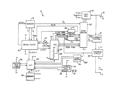
In Fig. 1, two wire transmitter 10 of the present
invention has a pair of terminals 12 and 14 which are
connected in a two wire current loop. The loop current IT
enters through terminal 12 and exits through terminal 14.
The magnitude of IT is controlled by current control 16 so
that the magnitude of IT bears a predetermined relationship
to a parameter sensed by sensor 18.
All of the electrical power used by transmitter 10
is derived from loop current IT. Voltage regulator 20
establishes potentials V+, VREF, and V-, which are used as
supply and reference voltages by all of the remaining
circuitry of transmitter 10.
13~C~924
-- 5 --
Current control 16 controls current IT
based upon a comparison of signal V8 with reference
Voltage VREF~ v8 is producad by integrator
circuit 22 based upon a sensor signal from sensor 18,
05 a pulse width modulated span adjusted feedback signal
(FB/SPAN) from analog switch array 24, and a pulse
width modulated zero signal (ZERO PWM) from
digital-to-analog converter (D/A) 26. Each of the
pulse width modulated outputs of D/A converter 26 is
generated by a solid state switching circuit such as
switching circuit 27 as shown in D/A converter 26.
~hese signals are combined and integrated to provide
a signal V8 which is controlled by means of
feedback through the current control to be
substantially equal to VREF such that IT = Iz +
KP.
In this embodiment, sensor 18 i8 a variable
reactance sensor which is driven by drive/clock
circuit 30. In addition to the drive signal provided
to sensor 18, drive/clock circuit 30 also provides a
clock signal ~CLOCK) to D/A converter 26 and a lower
frequency clock signal (CLOCK2) to microcomputer 32.
Microcomputer 32 receives input data from
communication input circuit 34 and stored digital
values from memory 36. Also associated with
microcomputer 32 i8 watchdog timer 38. ~ransmitter
provides span, zero, temperature correction and
third order linearity analog correction signals based
upon digital correction values stored in memory 36.
Microcomputer 32 controls D/A converter 26 as a
function of the digital correction values by
providing digital inputs to D/A converter 26.
13~)Q92~
-- 6 --
In this embodiment, D/A converter 26 is a
multi-channel digital-to-analog converter which is
driven by the CLOCK signal and which provides pulse
width modulated outputs which have duty cycle~ -based
05 upon corresponding digital inputs received from
microcomputer 32. In this particular embodiment, D/A
converter 26 has eight output channels, three which
are used for zero correction (ZEROPWM), three which
are used for span (SPANPWM~, one which is provided to
drive/clock circuit 30 through thermistor network 31
to provide span temperature compensation (STCPWM) and
one which is provided to analog switch array 24 to
provide third order linearity corrections ~3LINPWM).
The ZEROPWM outputs from D/A converter 26
are provided to integrator circuit 22 where they are
integrated and combined to form a part of signal V8.
The three SPANPWM outputs are provided to
analog switch array 24, where they are co~bined with
the feedback signal (VFB) from feedback circuit
28. The result is three ~ignals which represent the
feedback signal pulse width modulated in accordance
with the three SPANPWM outputs. These three combined
feedback/span signals (FB/SPAN) are provided to
integrator circuit 22.
The third order linearity pulse width
modulated signal (3LINPWM) is combined with a signal
from drive/clock circuit 30 by analog switch array 24
to produce a signal (3LIN) which is fed back to
drive/clock circuit 30. The 3LIN signal is used to
control the average frequency of the drive signal
8uppl ied to sensor 18 to achieve third order
linearity correction of the sensor signal.
13V09Z4
Communication input circuit 34 provide~
means by which a technician can communicate with
microcomputer 32 to change the digital correction
values stored in memory 36. Communication input
05 circuit 34 can take a variety of forms, including
magnetically actuated reed switches shown at 35 which
are activated with a magnet 37 from outside of the
transmitter by the technician. In this embodiment,
no external calibration devices are required, since
the magnetic signals can be sent directly through the
housing of the transmitter. Communication input
circuit 34 is, in another embodiment, a
multi-terminal connector which connects an external
device (such a~ the devices shown in Figs. 3-5) with
microcomputer 32. In still other embodiments,
communication input circuit 34 i8 connected to the
terminals 12 and 14 to sense encoded data which is
superimposed on the loop current IT. In that
embodiment, communication input circuit 34 includes
circuitry for converting the superimposed signals to
a format which can be accepted by microcomputer 32.
A comparator circuit 39 compares VFB to
VREF and provides signals to microcomputer 32
representative of zero and full scale current levels
80 that the microcomputer 32 can make automatic zero
and span adjustments of the output current IT.
The transmitter 10 shown in Fig.
eliminates the need for resistive potentiometers or
other variable or precisely selected circuit
components in order to provide calibration. Instead,
the present invention uses microcomputer 32 to simply
operate on D/A converter 24 to produce analog
correction signals which are then used ~y the analog
130C~924
signal processing circuitry of two wire transmitter
10. This provide~ high accuracy in the corrections
which are made, without the need for high precision
electrical components. In addition, the use of
05 digital values stored in memory 36 provides much
greater stability than would be achieved using
conventional potentiometers.
Transmitter 10 of the present invention also
has significant advantages over approaches where the
signal is converted from analog to digital, is
corrected, and then is converted back to an analog
signal. First, the output i~ not subject to alia~ing
error~ becau~e the analog ~ensor signal i~ never
sampled. Second, the output of transmitter 10 is
continuous and does not have resolution limits due to
quantization. Third, microcomputer 32 ic not
involved in real time measurement and therefore can
be run at a very low frequency. This reduces the
power requirements of microcomputer 32, which is an
important consideration in low power, two wire
transmitter circuitry. Fourth, because microcomputer
32 is not involved in the real time measurement
process, but simply provides digital values to D/A
converter 26 based upon stored correction values in
memory 36, it can be used for other tasks such as
communications. The microcomputer 32 can thus
calculate digital values provided to the D/A
converter at a low speed or rate compatible with low
power consumption while the analog output can provide
the output at a faster rate. Since the microcomputer
32 does not perform real-time calculation of the
output, the rate at which the microcomputer 32
updates the D/A converter 26 doe~ not limit the speed
13~ 9Z4
of the output. Also, since the sensor current I~
is not sampled by the processor, al~asing (also known
as heterodyning or beating) between the sensed
parameter and the sampling rate are avoided. This
05 will be discussed further in relation to the
embodiment shown in Fig. 6.
Figs. 2A and 2B is an electrical schematic
diagram showing the transmitter 10 of Fig. 1 in
further detail. Current control 16 is formed by
diode 40, PNP transistor 42, and operational
amplifier (op amp) 44. Diode 40 has its anode
connected to terminal 12 and lts cathode coupled to
the emitter of transi~tor 42. Diode 40 provides
reverse polarity protection in the event that the
voltage across terminals 12 and 14 is inadvertently
reversed. As shown in Fig. 1, terminal 12 is the
more positive terminal (designated with a "+") and
terminal 14 i8 the more negative terminal (designated
- by a "-"), 80 that the flow of loop current IT is
into terminal 12 and out of terminal 14.
The current flowing through current control
transistor 42 is controlled by op amp 44, which is
part of an LM10 integrated circuit 45 manufactured by
National Semiconductor. Op amp 44 receives a
reference voltage VREF at its inverting (-) input
and the variable signal Vs at it noninverting (+)
input. The output of op a~p 44 drives the base of
transistor 42 to achieve a balance condition in which
Vg and VREF are substantially equal. Zener diode
49 and resistor~ 51 and 53 provide current limiting
of the output stage to prevent excess current output
and prevent oscillations.
13()~?924
-- 10 --
Voltage regulator 20 includes operational
amplifier 46, band-gap circuit 47, resistors 48, 50
and 52 and capacitors 54, 56, and 58. Comparator 46
and band gap reference 47 are part of the LM10
05 integrated circuit 45. Voltage regulator 20
establishes a constant potential between line 60 and
line 62. As shown in Figs. 1 and 2, line 60 is
designated as V+ and line 62 as V-. The potential
between lines 60 and 62 is, in one embodiment, five
volts. Resistors 48, 50 and 52 form a voltage
divider between lines 60 and 62 to provide the
reference voltage VREF and to provide a feedback
voltage to operational amplifier 46. Capacitors 54,
56 and 58 are bypass capacitors which help stablize
the operation of voltage regulator 20.
Integrator circuit 22 includes resistors 64,
66, 68, 70, 72, 74 and 76 and capacitor 78.
Integrating capacitor 80 and resistor 81 provide A.C.
feedback to stabilize the loop. The ~ensor current
18 i~ summed, at node 82, with three span adjusted
feedback currents from analog switch 24 and three
pulse width modulated zero currents from D/A
converter 26. The summed current i8 filtered by
capacitor 178 and then provided to the RC integrator
formed by resistor~ 76 and 81 and capacitor 80 to
produce voltage Vs at the noninverting input of op
amp 44.
Feedback circuit 28 includes resistors 84,
86, 88, 90 and 92 and op amp 94. Resistor 84 i~
connected between line 62 and terminal 14, and acts
as the current feedback resistor~ The voltage
established across re~istor 84 i8 converted by
resistors 86, 88, 90 and 92 and op a~p 94 to produce
13~)~92~
a voltage VFB which is supplied to input ter~inals
of analog switches 96, 98, and 100 of analog switch
array 24. In the embodiment shown in Fig. 1, analog
switch array 24 is preferably a type CD4066B
05 integrated circuit analog switch array made by RCA
having four analog switches 96, 98, 100 and 102.
ll~e control terminals of switches 96, 98 and
100 are connected to outputs of D/A converter 26
which provide individual pulse-width-modulated span
signals. The outputs of switches 96, 98 and 100 are
connected through resistors 64, 66 and 68,
respectively, to summing node 82. The results are
three individual feedback currents which are a
function of a eedback voltage VFB modulated by the
15 individual pulse width modulated span signals.
In a preferred embodiment of the present
invention, D/A converter 26 is a type uA9706
multi-channel digital-to-analog converter made by
Fairchild which produces pul~e width modulated
20 outputs. Each output channel has six bits
resolution. To provide very high span and zero
resolution, three weighted outputs are used for span
and three weighted outputs for zero. The weighting
of the channel is a 26 relationship (or 64 to 1).
25 qq~ree channels thus provide 18 bit resolution. The
weighting of the channels i8 set by selection of the
resistances of resistors 64, 66, 68, 70, 72 and 74.
The three pulse width modulated span signal are
individually controlled, as are the three pulse width
30 modulated zero signals.
In the embodiment shown in Figs. 2A and 2B,
sencor 18 is an AC reactance type differential
pressure sensor cell, which has a pzir of capacitors
13(~C1 9Z~
- 12 -
Cl and C2, at least one of which i8 variable in
response to a parameter such as pre~sure. A drive
signal i8 received at the center plate of capacitors
Cl and C2, and a rectifying circuit formed by diodes
05 106, 108, 110, and 112 derive a sensor signal IS
which is supplied to node 82 of integrator circuit 22
and currents Il and I2 which are used by
drive/clocX circuit 30 in controlling the drive
~ignal supplied to capacitor~ Cl and C2. Drive/clock
circuit 30 maintains the drive to sensor 18 90 that
the product of the average frequency f, the peak to
peak voltage Vpp, and the sum of the capacitances
of Cl and C2 are constant:
fVpp (Cl + C2) K. Eq. 1
By maintaining this dri~e signal relationship, the
sen~or current I8 has the following relationship:
Equation 2:
IS 2~ (Cl - C2)/(Cl + C2). Eq. 2
Drive/clock circuit 30 includes a system
clock 114 formed by NAND Schmitt trigger gate 116,
resistor 118, crystal 119 and capacitor 120 which
provides clock signals for D/A converter 26,
microcomputer 32, as well a~ for drive/clock circuit
30. The output of NAND gate 116 is supplied to one
input of Schmitt trigger NAND gate 122. The output
of gate 122 is connected through resistor 124 and
capacitor 126 to the center plate of sensor
capacitors Cl and C2. The output of gate 122,
therefore, represents the drive signal which is
controlled in accordance with Eq. 1.
In the embodiment of the pxesent invention
shown in Figs~ 2A and 2B, the average frequency of
the drive signal is controlled by selectively
13(~ Z~
- 13 -
dropping out pulses from the clock signal supplied by
system clock 114 to gate 122. This selective
dropping out of signal pulses controlled by the
control signal supplied to the other input of gate
05 122. This control signal is provided by the
circuitry which include~ op amps 128 and 130, diodes
132, 134, and 136, resistors 138, 140, 142, 144, 146,
lS0, 152, 154, and 156, and capacitors 158, 160, 162,
164, 166, 168, and 170 and temperature sensitive
resistor network 148.
Current Il which flows through diode 106
is fed to the minus input of op amp 128. Resistors
144 and 146 act in conjunction with op amp 128 to
convert current Il to a current which is flowing
into node 171, which is conne~cted to the - input of
op amp 130. This current is summed with the current
I2 from diode 112 at node 171. As a result, node
171 has a potential which is proportional to Cl +
C2. The voltage at node 171 i8 compared to VREF by
op amp 130. The output of op amp 130 controls gate
122 to determine whether a particular clock pulse
from clock circuit 114 will pass through gate 122 to
sensor 18.
Span temperature compensation i8 provided by
applying the desired PWM voltage signal to
temperature sensitive resistor network 148. This
provides a correction current to node 171 at op-amp
130 which controls sensor excitation.
Third degree linearization is provided. A
signal from node 172 (which i8 the junction of
resistor 138 and capacitor 160) is supplied to the
input terminal of analog switch 102. The ~tate of
switch 102 is controlled by an output from D/A
130~3Z4
converter 26, which represents a pulse width
modulated signal having a duty cycle representative
of a desired amount of third degree linearization.
The output of switch 102 is fed back through
05 resistors 140 and 142 to node 171.
In tran~mitter 10 shown in Fig. 1, D/A
converter 26, microcomputer 32, and the drive for
~ensor 18 all are derived from a common clock signal
produced by system clock 114. Thi~ eliminates
possible alias or beat frequencies which could occur
if microcomputer 32 were operating on a separate
clock from that of the drive circuit. The system
clock signal is provided directly to the clock input
of D/A converter 126. In the case of microcomputer
32, however, the system clock is divided by counter
174 to produce a lower frequency clock signal
(CLOCK2) to the microcomputer 32. One of the
advantages of the transmitter of the present
- invention is that microcomputer 32 does not perform
computations or control functions in real time, and
therefore the CLOCK2 signal can be relatively low
frequency. This reduces the power requirements of
microcomputer 32, which is an important consideration
in a two wire transmitter which is powered solely by
the loop current I~. Microcomputer 32 preferably
comprises a type COP326C made by National
Semiconductor.
Watchdog timer 38 is formed by Schmitt NAND
gate 176, diodes 183 and 185, capacitor 178, and
resistors 180 and 181. Watchdog timer 38 resets
microcomputer 32 if it does not receive a ~ignal from
microcomputer 32 within a predetermined time period.
In addition, watchdog timer 38 resets microcomputer
32 when the power is first turned on.
13VC~9Z~
- 15 -
Microcomputer 32 receives digital correction
values from non-volatile memory 36 over the serial
input (SI) line and provides digital values to D/A
converter 26 over its serial output (S0) line.
05 Inverter 182 provides compatability between
microcomputer 32 and D/A convertor 26. Microcomputer
32 couples chip select (CS, CSl, CS2, CS3) signals to
access D/A 26, memory 36, and communication circuit
34.
In addition, microcomputer 32 receives input
values over the serial input line from communication
input 34 (which in this embodiment is a multi-pin
connector), and write~ new digital correction values
into memory 36 over the serial output line.
Use of serial communication between
microcomputer 32, D/A convertor 26, communication
input 34 and nonvolatile memory 36 minimizes pin
counts of the individual component~. Since speed is
not a significant consideration in the operation of
microcomputer 32, the reduced pin count and
simplification of connections among the components
provided by serial data transmission is an important
consideration.
Although transmitter lO of the present
invention offers significant advantages even if
adju~tment by a technician of correction factors such
as span and zero is not provided (i.e. the digital
values stored in memory 36 are factory set), it is
desirable to have a low cost device which would allow
the technician to adjust and configure two wire
transmitter 10 in the field. Previously available
hand held terminals used with conventional two wire
transmitters typically have been bulky and expensive.
13~C~924
- 16 -
Figs. 3 and 4 ~how a simple device that
functions in a manner similar to the potentiometer
controls that are familiar to instrument technicians,
yet provides digital values to microcomputer 32.
05 Electronic screwdriver 200 has a shank 202 of a~
electrically nonconductive material having a six
contact telephone type connector 204 at its distal
end. Rotatable function selecting ring 206 has a
window 208 which is aligned with one of eight
different functions which can be selected by the
technician. The screwdriver body 210 iB rotatable
about the central a%is. At its end, body 210 has a
calibration scale 212 which runs from zero to 100
percent. Scale 212 repre~ents the percentage of
maximum calibration value being selected by the
technician. Also located at the end of body 210 i8 a
push button 214 which is depressed to enter data.
As shown in Fig. 4, electronic screwdriver
200 includes a two channel, serial out, eight bit
analog-to-digital (A/D) converter 216 (such as a part
number COP432 made by National Semiconductor) which
is connected to six contact connector 204 so that
when connector 204 i8 connected to communication
input 34 of transmitter 14, AtD converter 216 is
powered by battery 217 and communicates with
microcomputer 32.
Function selection ring 206 is coupled to an
eight position switch 218 which contains three switch
contacts 218A-21BC connected through resistors 220,
222, and 224 to channel CHO of A/D converter 216.
Resistor 226 is connected between the CH0 input and
ground. Depending on the particular setting of
selector ring 206, one or more of the switch contacts
130~9Z4
218A-218C of switch 218 will be closed. When the
enter button 214 is pushed, it closes pushbutton
switch 228, which provides +5 volts to switch 218.
The voltage appearing at the CHO input of A/D
05 converter 216 will depend on the particular switch
contacts 218A-218C which are closed. Eight di~ferent
voltage levels can appear at CHO depending on the
position of function selection ring 206.
Input channel CHl of A/D converter 216 i9
connected to a single turn potentiometer 230. The
rotation of body 210 changes the setting of
potentiometer 230, and thus the voltage appearing at
CHl.
To u~e electronic screwdriver 200, the
operator insert~ connector 204 into the mating female
connector of communication input 34. The technician
then selects the function desired by rotating the
function ~election ring 206 until the desired
function appears in window 208. In the embodiment
~hown in Fig. 4, the functions which can be selected
include COARSE, MEDIUM and FINE ZERO; COARSE, MEDIUM
and FINE SPAN; SAVE; and OFF.
Once the technician has selected the desired
function, the enter button 214 is depressed. This
closes pushbutton switch 228, which allows A/D
converter 216 to read the voltage at CH0.
Microcomputer 32 reads CH0 and ~elects the
appropriate internal adjustment register in its
on-board random access memory (~AM).
The technician then adjusts the calibration
value by rotating body 210 until a cursor on button
214 is lined with the desired percentage on ~cale
212. As body 210 is rotated, data is continuou~ly
130C)~2~
-- 18 --
being provided, in the form of eight bit readings
from channel CHl to the selected channel of the D/A
converter 26 and the on-board RAM of microcomputer
32. When the adjustment is completed, the technician
05 can ~elect another function by changing the setting
of function select ring 206 and again pressing the
enter button 214. The technician then again performs
the adjust function by rotating body 210 to the
de~ired position and data is stored in the
10 appropriate register by microcomputer 32.
Up to this point, the data which has been
entered is stored only in the on-board memory of
microcomputer 32. To ~ave that data in nonvolatile
memory 36, the technician places the function select
15 ring 206 to the "Save" position and pushes the enter
button 214. This signals microcomputer 32 that it
should write the data stored in its internal
adjustment registers into the appropriate locations
of nonvolatile memory 36. At thi~ point, the
20 operation is completed, and the electronic
screwdriver 200 is di~connected from communication
input 34.
In another embodiment, the OFF function is
replaced by a FACTORY CALIBRATE function on function
25 selector ring 206. In this function, the operator
can select the original factory calibration simply by
moving the function selection ring to the FACTORY
CALIBRATE position and pressing the enter button
214. This allows the technician to always return the
30 unit to factory calibration regardless of the field
adjustments which have been made to calibration.
In some cases, it is desirable to restrict
the type of adjustments to be made by a particular
130~9Z4
-- 19 --
technician--for example, certain technicians may be
allowed to adju~t both zero and span, while other
technicians are permitted to adjust only zero. This
can be achieved by issuing different electronic
05 screwdrivers to different technicians, some which
have the span function settings while others do not.
Fig. 5 shows another embodiment of an input
device which operates in a manner similar to the
electronic screwdriver of Figs. 3 and 4, but provides
more complex functions to be performed. In this
embodiment, a digital interface circuit 240
communicates with microcomputer 32 through a
multi-terminal connector 242. The inputs to
interface circuit 240 include an enter push button
~witch 244, function ~elect switch 246, and a digital
value input which i~ preferably an array of BCD or
HEX encoded switches used for entering numerical
values .
The functions provided by function select
switch 246 include "ELEVATE ZERO", "SUPRESSED ZERO",
"SPAN", "LINEARITY", "CHARACTERIZE CELL",
"CHARACTERIZE CIRCUIT BOARD", "SAVE" and "OFF". To
calibrate, the technician sets the function switch
246 to, for example, "SPAN" and enters the desired
span in percent of maximum span by setting a value on
digital switches 248. The value is entered into
microcomputer ~2 by depressing enter switch 244. The
data which has been entered can be saved in
nonvolatile memory 36 by moving function switch 246
to the save position and again depressing the enter
button 244.
To repair transmitter 10, six-character
codes from the cell and circuit board assembly are
13(~C~924
- 20 -
entered using the CHARACTERIZE CELL and CHARACTERIZE
CIRCUIT BOARD functions. This permits the
microcomputer 32 to produce and store appropriate
calibration values to match the cell (i~e. the
05 sensor) to the circuit board.
Fig. 6 shows a block diagram of another
embodiment of the two wire transmitter of the present
invention. As in the embodiment ~hown in Fig. 1, two
wire transmitter 300 of Fig. 6 controls the loop
current IT flowing through terminals 302 and 304 as
a function of a parameter sensed by a sensor 306.
Analog transducer circuitry 308 controls the
magnitude of loop current ~T as a function of a
sensor ~ignal from sensor 306, together with span,
zero, linearity, and temperature compensation signal~
provided by microcomputer 310 through
digital-to-analog converter 312. The analog
correction values are based upon stored digital
correction values which microcomputer 310 obtains
from memory 314. In the embodiment shown in Fig. 6,
clock 316 provides clock signals to microcomputer 310
as well as D/A converter 312. In this preferred
embodiment, the outputs of D/A converter 312 are
pulse width modulated signals having duty cycles
which are determined by digital values provided to
D/A converter 312 by microcomputer 310.
Transmitter 300 includes a temperature
sensing resistor 318. Temperature compensation
circuit 320 senses the voltage on temperature sensing
resistor 18 and compares that voltage to one output
channel of D/A converter 312. The output ba~ed on
this comparison is provided to microcomputer 310~ By
changing the digital value provided to D/A converter
13~924
- 21 -
312, microcomputer 310 can determine the digital
value w~ich causes the output of circuit 320 to
change state. That digital value i8 repregentative
of the sensed temperature. Microcomputer 310
05 provides appropriate digital values to A/D converter
312 based on the sensed temperature to temperature
compensate the analog transducer circuitry 308. This
includes a temperature compensation signal output
from A/D converter 312, and may also involve
adjustment of some or all of the other outputs of
A/D converter 308. The constants for this
temperature compensation are stored in nonvolatile
memory 314.
Transmitter 300 include~ provision or
communication between microcomputer 310 and a remote
terminal over the two wires connected to terminals
302 and 304. This communication is achieved by
superimposing ~erial communication signals on the
loop current IT flowing through transmitter 300.
Incoming communications are detected by communication
input detector 322, which converts the fluctuations
in the loop signal into serial data supplied to the
serial data in port of microcomputer 310. Outbound
communications from microcomputer 310 are supplied
through communication output circuit 324, which
drives the current controller of the analog
transducer circuitry 308 to superimpose serial
communication signals on the loop current.
Preferably, the remote terminal 307 with
which microcomputer 310 communicates i~ capable of
measuring loop current as well as communicating.
This facilitates calibration, since microcomputer 310
otherwise doe~ not have available the value of the
~3()~924
- 22 -
loop current at any given point in time. A diode 30~
in the loop can provide a third terminal to the
remote terminal 307 for measuring loop current.
Current can thu~ be measured without interrupting the
05 loop current. If desired, this three terminal
connection can provide power to remote terminal 307
while still allowing it to monitor transmitter output
current.
In conclusion, the present invention is a
two wire transmitter which i8 similar in size, cost,
and performance to totally analog tran~mitter
circuits. The addition of digital circuitry and a
microcomputer achieves high resolution calibration,
increases flexibility and ease in the selection of
calibration values and the recalibration of the
transmitter, and provides greater stability than is
achieved using adjustable analog devices (such as
adjustable potentiometers and variable capacitances)
in order to achieve calibration of the transmitter
circuit.
Although the present invention has been
described with reference to preferred embodiments,
workers skilled in the art will recognize that
change~ may be made in form and detail without
departing from the spirit and scope of the invention.