Note: Descriptions are shown in the official language in which they were submitted.
130~2~d~
COAXIAL HYBRID COUPLER AND CROSSING ELEMENT
BACKGROUND OF THE_INVENTION
Microwave circuits are employed for coupling
electromagnetic energy between microwave components such
as horns, circulators, signal generators and receivers.
The conduits by which the electromagnetic energy is
coupled between the microwave components may be
constructed in various forms of transmission lines
ranging from stripline to waveguide, and frequently
includ~ various forms of power couplers, power
splitters, and power combiners. Such conduits allow
microwave signals to be split among a number of mi-
crowave components, and also allow the combining of
signals from a plurality of microwave components.
Of particular interest herein are complex microwave
circuits employing coaxial transmission lines,
particularly rigid coaxial transmission lines having a
center conductor of rectangular or square cross section,
for interconnecting numerous microwave components. Such
circuitry is found, by way of example, in large antenna
arrays employing many horn radiators coupled by signal
combiners and/or splitters to produce a desired
radiation pattern. In such complex microwave
~3UlZ64
1 structures, it is frequently necessary to bring signals
~rom various parts of the structure to other parts o~
the structure by coaxial lines which cross over each
other. An example of such routing of signals is found
in a matrix of interconnected signal pathc such as a
Butler matrix employed in converting a signal input at
one port of the matrix to a set of signals outputted by
the matrix for forming a beam. The crossings of signals
in such matrix structures have been accomplished,
heretofore, by bending one transmission line about
another.
A problem arises in that the complexity and size of a
microwave structure i8 increased by signal crossovers
employing a bending of one coaxial transmission line
about another. It is recognized that a simplified form
of such a structure is attained by placing all
components and connecting transmission lines in a
single plane. However, a multiplicity of crossovers
comprising bent transmi3sion lines can produce a
considerable amount of stacking of the transmission
lines, one above the other. Such a mechanical
configuration is both bulky and heavy. Excessive bulk
and weight are characteristics which are to be avoided
in the construction o~ antenna arrays, such as those
employed in satellites, wherein a reduction in space and
weight is most desirable.
SUMMARY O~ THE INVENTION
The foregoing problem is overcome and other advantages
are provided by a coaxial transmission-line crossover
which, in accordance with the invention, can be
con~tructed without necessitating any increased height
~301264
1 to the crossover structure as compared to that of an
individual coaxial line. This permits the microwave
circuit to be con~tructed in a planar microwave
configuration.
s
In accordance with the invention, an in-plane-
configuration for a microwave crossover is attained by
connecting two hybrid couplers in tandem wherein each of
the hybrid couplers divides the power of an incoming
electromagnetic wave into two waves of equal power with
a 90 degree phase shift between the two waves. Each of
the hybrid couplers has two input ports and two output
ports, the output ports of a first one of the two
couplers being connected to the input ports of a second
one of the two couplers.
The arrangement of the interconnection of the two
couplers is accomplished by constructing all conduits of
electromagnetic power within a single planar
configuration, in accordance with a feature of the
invention, by use of a coupler having two input ports on
a front side of the coupler and two output ports on a
back side of the coupler. Such a coupler is constructed
by use of coaxial transmission lines connecting to the
ports of the coupler and whereln, within a housing of
the coupler, diametrically opposed pairs of input and
output ports are connected by a pair of crossed
insulated, electrically-conducting rods or bars which
are spaced apart by a uniform narrow gap to prsvide for
capacitive coupling of electromagnetic power between the
two bars.
1301264
1 In accordance with yet another feature of the invention,
an inplane configuration for the crossing of the two
bars is attained by the construction of a notch in a
central region of each bar, the notch of one bar facing
the notch of the other bar at the site of the crossover
with one notch engaging with and enveloping the other
notch while maintaining a gap between the walls of the
notch, through which gap there is capacitive coupling of
electromagnetic power. The effect of the crossover has
the effect of creating a half twist to the two bars, in
a manner similar to a twisted pair of electrical
conductors, this resulting in a relocation of one input
port and one output port so as to place both input ports
on the front side of the housing and both output ports
on the back side of the housing.
Two embodiments of the crossed configuration of the pair
of bars within a metallic housing are provided. In a
first embodiment, each of the bars is provided with a
pair of end portions which extend transversely to the
housing, the end portions being joined by a central
portion which is angled at approximately 45 degrees to
offset the two end portions and to provide opportunity
for the crossing of one central portion over the other
central portion. The end portion of one bar are
parallel to the corresponding end portions of the other
bar to provide for capacitive coupling of
electromagnetic power therebetween. A rectangularly
shaped notch is provided in each of the central portions
of sufficient size to provide for a desired gap width
between the central portions in the crossover region for
capacitive coupling of electromagnetic power between the
central portions, which capacitive coupling per unit of
130~26~
1 length of a bar is substantially the same as the
capacitive coupling per unit length of the bar at the
end portions, thereby to minimize any tendency to
develop reflected waves at the crossover. The overall
length of the bars is approximately one-quarter
wavelength of the radiation, with the central portion
being less than one-tenth of a wavelength of the
radiation.
In a second embodiment, both of the bars are replaced
with bars ha~ing tapered extensions beyond the foregoing
end portions, the extensions being inclined throughout
their length, with a central portion parallel to the
extensions and inclined to the two end portions. The
resulting zig-zag configuration allows opposed end
portions of the bars to be parallel to each other and to
allow the crossing of one central portion over the other
central portion. The notches in the central portions
have a generally rectangular form with the end walls of
the notches being stepped for increased bandwidth of the
coupler. In addition, sections of sidewalls of the bars
which face each other are angled relative to a central
axis of the bar to establish a uniform gap width between
these sidewall sections for a predetermined amount of
capacitive coupling of electromagnetic radiation. In
each bar, the central axis is parallel to each of the
end portions, the end portions being offset to opposite
sides of the central axis, while a narrow strip or
isthmus of the central portion is parallel to and
disposed on the central axis. This configuration of the
bars increases the bandwidth of the coupler. Dielectric
supports are positioned transversely of the housing on
both sides of the crossed central regions, and a
~301;~6~
positional dielectric spacer is placed within each gap
formed between opposed end portions on opposite sides of
the engaging notches of the central portions. In both
embodiments, the bars have a rectangular or square
cross-sectional form.
Other aspects of this invention are as follows:
A coaxial transmission-line crossing element
comprising:
a first hybrid coupler and a second hybrid coupler,
each of said couplers having a first input port, a
second input port, a first output port, and a
second output port; and wherein
said first output port of said first coupler is
connected to said first input port of said second
coupler, said second output port of said first
coupler is connected to said second input port of
said second coupler, said first and said second
input ports of said first coupler serving as input
ports of said crossing element, and said first and
said second output ports of said second coupler
serving as output ports of said crossing element;
and wherein
each of said couplers comprises:
a housing of electrically conductive material
having a top wall and a bottom wall, there being a
front wall, a back wall, a first sidewall and a
second sidewall joining said top wall to said
bottom wall, said housing having four openings
oriented normally to a common plane, said top wall
and said bottom wall being parallel to said common
130~Z~i4
6a
plane, said openi.ngs being positioned serially
around a center of said housing and pointing
outward in different directions;
center conductors disposed in each of said openings
to form therewith said input ports and said output
ports, said first input port and said first output
port being located at opposite ends of said first
sidewall, said second input port and said second
output port being located at opposite ends of said
second sidewall, said first input port and said
second input port being located at opposite ends of
said front wall, and said first output port and
said second output port being located on opposite
ends of said back wall;
a pair of bars electrically connecting ports of
said first sidewall with ports of said second
sidewall, said bars being uniformly positioned
apart from each other and from an inner surface of
said housing; and
means for twisting a first bar of said pair of bars
about a second bar of said pair of bars with a half
twist to enable said first bar to interconnect said
first :input port with said second output port, and
to enable said second bar to interconnect said
second input port with said first output port.
A coupler for electromagnetic power comprising:
a housing of electrically conductive material
having a top wall and a bottom wall, there being a
front wall, a back wall, a first sidewall and a
second sidewall joining said top wall to said
bottom wall, said housing having four openings
oriented normally to a common plane, said top wall
26~
6b
and said bottom wall being parallel to said common
plane, said openings being positioned serially
~round a center of said housing and pointing
outward in different directions,
center conductors disposed in each of said openings
to form therewith a first input port and a second
input port and a first output port and second
output port, said first input port and said first
output port being located at opposite ends of said
first sidewall, said second input port and said
second output port being located at opposite ends
of said second sidewall, said first input port and
said second input port being located at opposite
ends of said front wall, and said first output port
and said second output port being located on
opposite ends of said back wall;
a pair of bars electrically connecting ports of
said first sidewall with ports of said second
sidewall, said bars being uniformly positioned
apart from each other and from an inner surface of
said housing; and
means for twisting a first bar of said pair of bars
about a second bar o~` said pair of bars with a half
twist to enable said first bar to interconnect said
first input port with said second output port, and
to enable said second bar to interconnect said
second input port with said first output port.
BRIEF DESCRIPTION OF THE DRAWING
The aforementioned aspects and other features of the
3~ invention are explained in the following description,
taken i~ connection with the accompanying drawing
wherein:
130~264
Fig. 1 is a plan view of the crossover of the invention
formed within a planar configuration of a metallic base
plate with a cover plate shown partially cutaway to
expose the central conductors of coaxial transmission
lines;
Fig. 2 is an end view of the crossover taken along the
line 2-2 in Fig. 1;
Fig. 3 is an enlarged plan view of a fragmentary portion
of one of two hybrid couplers of the crossover of Fig. 1;
Figs. 4 and 5 show sectional views taken along lines 4-4
and 5-5, respectively, in Fig. 3 to show details of bars
in the crossover region of one of the couplers of the
crossover;
',~
130126A~
1 Fig. 6 is a view, similar to that of Fig. 3, showing an
alternative embodiment of the crossover region of a
coupler;
Fig. 7 and 8 show, respectively, a plan view and a side
view of a bar in the alternative embodiment of the
coupler of Fig. 6; and
Fig. 9 is a diagrammatic representation of the tandem
arrangement of the two couplers of Fig. 1 including
paths of electromagnetic waves useful in explaining
operation of the crossover.
DETAILE~ DESCRIPTION
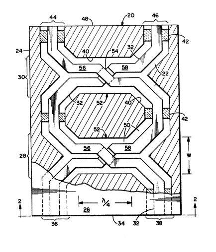
Figs. 1 and 2 show a crossover 20 formed of coaxial
trancmission lines 22 disposed within a base plate 24
covered by a cover plate 26. In accordance with the
invention, the crossover 20 comprises two hybrid
couplers 28 and 30 which are formed of crossed sections
of a center conductor 32 of coaxial lines 22. Fig. 2
shows a front end 34 of the crossover 20, the view of
Fig. 2 showing a first input port 36, a second input
port 38, and the cover plate 26 disposed on top of the
base plate 24. In Fig. 1, a portion of the cover plate
26 is shown, and the balance of the view is shown
sectioned beneath the top surface of the base plate 24,
as indicated in Fig. 2. The sguare cross section of
center conductors 32, as well as the the square cross
section of the inner surface of the outer conductor 40
of the transmission lines 22 are also shown in Fig. 2.
It should be noted that, while the square cross
sectional configuration of the transmission lines 22 is
~L3~)~264
1 employed in the preferred embodiment of the invention,
the teaching~ of the invention are applicable also to
rectangular coaxial transmission lines. Dielectric
supports 42 position the center conductors 32 within the
outer conductors 40 and insulate the center conductors
from the outer conductors. To facilitate the
description in Fig. 1, only a few of the supports 42 are
shown, it being understood that such supports may be
positioned in various locations along the transmission
lines, and may be given a well-known physical
configuration which negates reflection of
electromagnetic waves.
Each of the hybrid couplers 28 and 30 provide for a
splitting of an electromagnetic wave into two waves of
equal power, wherein the two waves differ in phase by go
degrees. As will be explained herein, each of the
couplers 28 and 30 are fabricated in accordance with a
feature of the invention which provides that two input
ports are located on a front end of each of the
couplers, and two output ports are located on the back
end of each of the couplers. By way of example, the two
input ports 36 and 38 of the crossover 20 also serve as
input ports to the coupler 28. A similar pair of output
ports, namely, a first output port 44 and a second
output port 46, are located at the back end 48 of the
crossover 20. The output ports 44 and 46 also serve as
output ports of the coupler 30. The couplers 28 and 30
are of identical construction.
As may be seen by the layout of the couplers 28 and 30
presented in Fig. 1, and by the end view presented in
Fig. 2, the coaxial transmis~ion lines 22 are fabricated
1301264
1 in a convenient fashion by milling out channels 50
within the kase plate 24 to provide the outer conductors
40 of the transmission lines 22. The center conductors
32 are then placed within the channels S0, and supported
in their respective positions by the supports 42.
Thereupon, the a~sembly is completed by installing the
cover plate 26 on top of the base plate 24. ~oth the
base plate 24 and the cover plate 26, as well as the
center conductors 32, may be fabricated of an
electrically conducting material which is readily
machined, such as aluminum.
As will be explained in further detail hereinafter with
reference to Fig. 9, the crossover 20 acts to couple an
electromagnetic wave from one of the input ports to the
diagonally opposite output port, for example, from the
second input port 38 to the first output port 44. This
is accomplished by virtue of the even splitting of power
at each of the couplers 28 and 30 with the phase lag of
90 degrees, this resulting in a cancellation of waves at
one of the output ports so that all of the power of the
input wave exits from the other output port.
It is noted that a particular feature of the invention
is the con~truction of the crossover 20 including all
components of the couplers 28 and 30 and their
interconnecting transmission lines 22 within a single
assembly of planar configuration. This is made possible
because of the presence of both input ports of a coupler
on the front end of the coupler, and the presence of
both output ports on the back end of the coupler. This
arrangement of the ports of each of the couplers 28 and
30 allows for the interconnection of the couplers via
1301Z64
1 the transmission lines 22 as shown in the layout of Fig.
1, the layout disclosing that all connections are
accomplished within a common planar configuration
without the need for any transmission lines located
outside of the asse~bly of Fig. 1. Both the plates 24
and 26 are of planar configuration and serve to form a
housing of planar configuration for the coupler 28 and
for the coupler 30.
These novel features are a direct consequence of the
novel construction of each of the couplers 28 and 30,
which construction will now be described in accordance
with the invention.
With reference to Figs. 1-5, the coupler 28 is formed
with a central region 52 having a crossover 54 of two
center conductors 32. Since both of the couplers 28 and
30 have identical construction, only the coupler 28 will
be described in detail, it being understood that the
description of the coupler 28 applies equally well to
the coupler 30. In the central region 52, each of the
center conductors 32 takes the ~orm of a bar, there
being two such bar~ 56 and 58 in the central region 52
and at the crossover 54. At the crossover 54, one bar
crosses above the other bar which, by way of example, is
portrayed in Fig. 3 by a crossing of the bar 56 above
the bar 58.
The crossover 54 is accompliched within the planar
configuration by notching each of the bars 56 and 58
with notches 60 which face each other and allow the bars
56 and 58 to pass through each other at the notches 60
within the confines of the thickness of the bar 56 and
~301264
1 the bar 58 as is shown in the side views of Figs. 4 and
5. The notches 60 are sufficiently large to provide for
clearance between the bars 56 and 58 at the crossover
54, the clearance maintaining electrical insulation
between the two bars 56 and 58.
In Fiq. 4, the bar 56 is shown to be notched at its
bottom side, while Fig. 5 shows that the bar 58 is
notched at its top side. As shown in Figs. 1 and 3, the
bars 56 and 58 are parallel to each other except at the
crossover 54 where each of the bars undergoes a 45
degree change in direction so as to cross the other bar
at an angle of 90 degree~. In each of the bars 56 and
58, the notch 60 i5 located at a crossing strip 62, the
crossing strip 62 introducing a reverse curve to the bar
by virtue of two turns of 45 degrees in opposite
directions. The depth of each notch 60 is somewhat
greater than the thickness of the rod 56, 58 so as to
provide clearance in the vertical direction between the
strips 62 of the two bars 56 and 58. Clearance is also
provided in the horizontal (parallel to the plane of the
base plate 24) direction between a strip 62 of one of
the bars and the sides 64 of the notch 60 in the other
of the two bars.
The clearance between the two crossing strips 62 at the
central portions of the bars 56 and 58, and clearance
between parallel end portions of the bars 56 and 58 are
selected to produce a desired amount of capacitance for
coupling electromagnetic power between the bars 56 and
58. At an operating frequency in the range of 3.7 - 4.2
GHz (gigahertz) wherein the free-space wavelength of the
radiation has a nominal value of three inches, the
130126~
1 clearance between the parallel end portions of the bars
56 and 58 is selected to define a gap 66 having a width
of 30 mils. A larger clearance is provided at the
crossover 54 such that the spacing between the crossing
strips 62 as well as between a crossing strip 62 and
sides 64 of a notch 66 are each equal to 50 mils. The
larger clearance at the crossover 54 reduces the
capacitance to the crossover 54 so as to equalize the
amount of capacitance per unit length of the bar 56 or
58 throughout the length of the bar including both the
end portion and the region of the crossover 54. It is
noted that, in the absence of such increased clearance
at the crossover 54, the added length of gap along the
sides 64 of a notch plus the bottom 68 of a notch 60
tends to increase the amount of capacitance at the
crossover 54. It is desired to maintain uniform
capacitance in the central region 52 of the coupler 28
so as to minimize reflection of electromagnetic waves
and insure a low value of VSWR (voltage standing wave
ratio). The foregoing increase of clearance at the
crossover 54 produces the desired reduction in the
capacitance at the crossover 54 so as to equalize the
capacitance per unit length of bar.
In term6 of operation of the coupler 28, the
configuration of the crossed bars 56 and 58 in Fig. 3
has the form of a twisted pair of electrical conductors
wherein only one half twist is provided. Therefore, the
two bars 56 and 58 may be viewed as a pair of parallel
bars through which electromagnetic power is coupled.
The location of input and output ports of the. coupler 28
follows the twisting of the bars 56 and 58. In
addition, the implementation of the twist, as is
~310~64
/~
1 provided by the crossover 54 maintains electromagnetic
coupling between the two bars 56 and 58 so that the
desired amount of coupled power is maintained,
independently of the twisting of the bars 56 and 58~
Thereby, the coupler 28 can provide for a division of
the electromagnetic power of a wave incident upon the
coupler 28 into two waves of equal power outputted from
the coupler 28 in substantially the same fashion as
though the bars 56 and 58 were totally straight. Thus,
by construction of the crossover 54 to implement a
twisting of the bars 56 and 58, the effect in the
operation of the coupler 28 is to interchange locations
of input and output ports, in accordance with the
invention, such that the two output ports are on the
same side, namely the back side of the coupler 28 while
the two input ports also share a common side, namely the
front side of the coupler 28. This provides the coupler
28 with the requisite locations of input and output
ports to allow the arrangement of interconnection
between the two couplers 28 and 30 in a planar
configuration as shown in Fig. 1.
It is also noted that, while the coupler 28 has been
described for use with the cro~sover 20, the coupler 28
2S may also be employed in other microwave circuits for
performing algebraic combinations of electromagnetic
signals. Since the coupler 28 is reciprocal in its
operation, it may be employed for both division of power
in one wave among two other waves, as well as for
combining the power of two waves into one wave. Also,
the above noted gap width which has been established for
a 3 dB coupling of power can be enlarged to provide for
a coupling of smaller amounts of power. In the
130~2~;~
14
1 preferred embodiment of the invention, the following
cross sectional dimensions of the transmission linss 22
are employed; the center conductor 32 in cross section
measures 0.2 inches on a side, and the outer conductor
40 in cross section measures 0.5 inch on a side. The
length of the bars 56 and S8, as portrayed in Fig. 1, is
one-quarter wavelength of the electromagnetic energy
propagating along the transmission line~ 22. The width
W (Fig. 1) of a channel 50 is enlarged at the coupler 28
to provide room for both of the center conductors 32,
the width being increased by the width of one outer
conductor 40. The form of electromagnetic wave
propagating along a coaxial transmission line 22 is a
TEM (transverse electromagnetic) wave. The impedance of
a transmission line 22 is 50 ohms.
Fig. 6 shows a view of a hybrid coupler 70 which is an
alternative embodiment of the hybrid coupler 28 of Fig.
1. The coupler 70 is fabricated in the same way as the
coupler 28, and is formed of a base plate 72 in which
channels 50 have been milled out to form the outer
conductors 40 of coaxial transmission lines 22, the
lines 22 including a center conductor 32, as was
disc10~6d in the construction of the hybrid coupler 28
of Fig. 1. rrhe view of Fig. 6 shows a layout of the
components of the coupler 70 and has been formed by
taking a section through the base plate 72 parallel to
the top surface thereof, as was done in the sectioning
of the view of Fig. 1.
In the event that the coupler 70 is to be employed in
the construction of a microwave crossover circuit, such
1301264
1 as the cros~over 20 of Fig.l, then the base plate 72
would be extended to include two of the couplers 70 with
interconnecting transmission lines 22 in the same
fashion as is disclosed for the construction of the
S crossover 20 of Fig. 1. The configuration of the base
plate 72, as shown in Fig. 6, suffices for the creation
of the two input ports 36 and 38, for each of the
couplers 70 and the two output ports 44 and 46 for each
of the two couplers 70. These ports may be employed for
connection of the coupler 70 to various microwave
circuits or components such as another hybrid coupler.
As was the case with the coupler 28, the input ports 36
and 38 of the coupler 70 are directed towards the front
of the coupler, while the output ports 44 and 46 of the
lS couplers 70 are directed towards the back of the
coupler. The cross sectional dimensions of the center
conductor 32 and the outer conductor 40 in each of the
transmission lines 22 are the same as that disclosed for
the coupler 28 of Fig. 1. It should be ncted that the
description of the construction of the coupler 70, as
well as of the coupler 28, can also be employed for
coaxial transmission lines in which the center
conductors have a nonrectangular cross~sectional shape
such as a circular or elliptical shape. However, the
rectangular shape i8 preferred for 3 dB couplers wherein
an input wave divideq into two output waves of equal
power.
The coupler 70 includes a central region 74 which
differs from the central region 52 of the coupler 28 by
the provision of a crossing strip 76 in each of two bars
78 and 80 which are narrower than the corresponding
crossing strips 62 in the bars 56 and 58 of the coupler
~30~264
16
l 28. The bars 78 and 80 of the coupler 70 (Fig. 6)
correspond respectively to the bars 56 and 58 of the
coupler 28 (Figs. 1 and 3~.
A further difference between the central region 74 and
52 is the provision in the central region 74 of a notch
82 in each of the bars 78 and 80 which has a stepped
sidewall 84 (Figs. 7 and 8) instead of the straight side
64 (Figs. 3, 4, and 5) of the notch 60. Yet a further
distinction between the central regions 74 and 52 is the
inclusion at the edge of the central region 74 of a
taper 86 (Figs. 6 and 7) on extension or wing portions
of the bars 78 and 80 approaching a crossover 88 (Fig.
6), such tapers being absent in the coupler 28 of Fig,
1. The foregoing differences in structure between the
couplers 70 and 28 provide the coupler 70 with a better
VSWR, and also increases the operating bandwidth of the
coupler 70 as compared to the coupler 28.
As may be seen by inspection of Figs. 6 and 1, the bars
78 and 80 have a more complex structure than the bars 56
and 58. It should be noted that the two bars 78 and 80
have the same physical shape, the geometry of the bar
80, as portrayed in Fig. 6, being obtained by turning
the bar 78 upside down. Specific details in the
con3truction of the bar 78 and 80 may be obtained by
reference to the detailed views of the bar 80 in Figs. 7
and 8. As the bar 80 extends inwardly from the
extensions thereof, the width of the bar 80 is reduced
by the taper 86 to a value of approximately one-half the
original width such that the width of the crossing strip
76 is approximately 0.1 inch, as compared to 0.2 inches
width at the ends of the bar 80. The crossing strip 76
~301;264
17
1 is joined by necks 90 (Fig. 7) which are angled relative
to the strip 76 so as to offset both extensions of the
bar 80 on opposite sides of a central axis 92 of the bar
80. Both extensions of the bar 80, and the strip 76 are
parallel to the axis 92, the strip 76 being centered on
the axis 92. Inclination o~ a neck 90 relative to an
extension of the bar 80 is shown in Fig. 7 by an angle
J equal to 135 degrees. The inclination of both of the
necks 90 to their respective bar extensions are the
same. Inclination of a taper 86 relative to a straight
edge of an extension of the bar 80 is shown in Fig. 7 by
an angle H equal to 22.5 degrees. Both of the tapers 86
in the bar 80 have the same inclination.
The crossover 88 (Fig. 6) is similar to the crossover
54 (Figs. 1 and 3) in that, in both cases, the crossing
strip of one bar is enveloped by the notch of the the
other bar. As may be seen in Figs. 7 and 8, a bottom 94
of the notch 82 is sufficiently wide to extend beyond
the side edges of the crossing strip 76 in the crossover
88 (Fig. 6). Steps of the stepped sidewalls 84 extend
still further back from the sides of the crossing strip
76 in the crocsover 88. Beyond the region of the
crossover 88 and the necks 90, the bars 78 and 80
broaden to their initial width. Thus, the necks 90 and
the crossing strip 76 can be viewed as an isthmus which
joins the broader extensions or wing portions of each
of the bars 78 and 80.
30 As ~hown in Fig. 6, the bars 78 and 80 are held in
position by means of two springs 96, two dielectric
supports 98, and a pair of dielectric spacers 100. The
springs 96 are secured within pockets 102 in a sidewall
130126A
18
l of a channel 50. The springs urye the supports 98
towards each other and against the bars 78 and 80. The
spacers 100 are oriented vertically with respect to the
plane of the base plate 72 and are disposed between
facing sides of paired necks 90, there being one spacer
100 on opposite sides of the crossover 88. The spacers
100 resist the forces exerted by the springs 96 as the
bars 78 and 80 are urged together, thereby tightly
holding the bars 78 and 80 in their respective positions
for maintaining a desired clearance between the necks go
of the bars 78 and 80, and between the corresponding
portions of the crossing strips 76 and the notches 82 at
the crossover 88, As was the case with gaps and
spacings disclosed above with reference to the coupler
28, corresponding values are employed in the coupler 70
of Fig. 6. Thus, the spacers 100 have a thickness of 30
mils, and the vertical spacing between the bottom 94 of
a notch ~2 and the facing side of a crossing strip 76 is
50 mils. With respect to the dimensions of the steps of
the stepped sidewall 84 (Fig. 8), the depth of the step
is approximately one-third the depth of the bottom 94 of
the notch 82, while the horizontal portion of the step
is approximately one-third the width of the bottom 94.
An iri8 lt)4 (Fig. 6) is provided by two vanes 106
extending inwardly towards the crossover 88 from outer
sidewalls of channels 50, the vanes 106 being coplanar
with the spacers 100. The iris 104 serves to limit the
region through which electromagnetic power from an input
port 36, 38 can couple to both of the output ports 44
and 46. The length of the foregoing isthmus (the two
necks 90 plus the crossing strip 76) is one-quarter
wavelength of the electromagnetic waves propagating
~L30~264
/q
l along the transmission lines 22, this length being less
than the cross-sectional dimension of the iris 104. In
terms of the operation of the coupler 70, it is noted
that the amount of power coupled between the bars 78 and
80 depends on the capacitance between the two bars, this
being determined primarily by the coupling at the
spacers lO0 and at the crossover 88, while the
difference in phase imparted between waves outputted at
the ports 44 and 46 is determined by interaction of
elec~romagnetic wave~ across the entire distance of the
iris 104. The material employed in the supports 98 and
the spacers 100 i5 preferably a plastic material having
a dielectric constant of approximately 3.2, one such
material being marketed by General Electric under the
trade name of ULTEM 1000, this material being
dimensionally stable, even at high temperatures.
operation of the crossover 20 of Fig. 1 constructed with
the hybrid couplers 28 and 30 is the same as the
operation of the crossover 20 with two couplers 70
substituted for the couplers 28 and 30. This operation
is explained with the aid of the diagrammatic
representation of Fig. 9 which shows the two couplers 28
and 30 wherein output ports of the coupler 28 are
connected via transmission lines 22 to corresponding
input ports of the coupler 30. Also shown in Fig, 9 are
the two input ports and the two output ports of the
crossover 20. In this explanation of the operation, it
i5 presumed that a wave enters the second input port at
point G, and propagates along paths indicated by dashed
lines. Key points on the dashed lines are indicated at
E and F in the coupler 28, and four waves resulting by
~301;~64
l operation of the couplers 28 and 30 appear at points A,
B, C, and D at the two output ports of the crossover 20.
In operationl the input wave at G splits at the coupler
28 into two waves E and F having equal power, which
power is equal to one-half of the original power at G.
The wave at E is shifted 90 degrees lagging relative to
the wave at F. At the coupler 30, the wave E splits
into two components B and C having equal power, the
power in the wave components B and C each being equal to
one-quarter of the input power at G. Similarly, the
wave at F is split by the coupler 30 into two wave
components A and D having equal power, the power in each
of the waves A and D being equal to one-quarter of the
power at G. The wave at C is shifted in phase by a
lagging ninety degrees relative to the wave at B.
Similarly, the wave at A is shiftad in phase by a
lagging 90 degrees relative to the wave at D. As a
result of the phase shifting, the wave component at C
has undergone two ninety-degree phase shifts for a total
phase shift of 180 degrees. Therefore, the wave
component C destructively interferes with the wave
component D resulting in a cancellation of all power
outputted at the second output port. Therefore, none of
the power of the wave at E iB coupled from the left side
of the coupler 30 to the right sida of the coupler 30:
all of the power at E exits the first output port.
Similarly, none of the power at F exits the second
output port, all of the power being coupled from the
right side of the coupler 30 to the left side of the
coupler 30 to exit at the first output port. Since the
coupling of power via the couplerc 28 and 30 each
introduce a lagging phase shift of 90 degrees, the
~301Z64
21
1 contributions via both couplers 28 and 30 are in phase
at the first output port, the two contributions at A and
B each having a lagging phase shift of 90 degrees.
Thus, the two contributions at A and B add cophasally to
produce an output power at the first output port equal
to the power inputted at the second input port. The wave
outputted at the first output port has a lagging phase
of ninety degrees relative to the phase of the wave
inputted at the second input port.
It is to be understood that the above described
embodiments of the invention are illustrative only, and
that modifications thereof may occur to those skilled in
the art. Accordingly, this invention is not to be
regarded as limited to the embodiments disclosed herein,
but is to be limited only as defined by the appended
claims.