Note: Descriptions are shown in the official language in which they were submitted.
`7~
Specification
Title of the Invention
Digital Communication Apparatus
Background of the Invention
The present invention relates to a digital
communication apparatus and, more particularly, to a
digital communication apparatus having a reception function
for detecting, validating, and monitoring reception
information.
In a digital communication system wherein a large
number of stations use an identical carrier wave to
interchange information, each station receives a unique
word transmitted from a predetermined station at a
predetermined period to set its own transmission/reception
timing, and transmits information signals with the unique
word at the set transmission timing, or receives
information signals with a unique word at the set reception
timing. In this case, in order to improve reliability of
information transfer, the information signals except for
the unique word are encoded into data having optimal
redundancy with respect to the unique word.
Such a digital communication apparatus is
disclosed in Japanese Patent Laid-Open No. 60-227542,
MIYAUCHI and NOSAKA, "Digital Satellite Communication", pp.
76 - 77 published in Japan, and Dr. Kamilo, et al.,
~3~ 7~
"~igital Communication", pp. 375 - 377 published in the
U.S.A.
However, various troubles may occur in this
system because of degradation in quality of communication
channels or the influence of thermal noise in the system.
For example, even if a received unique word is correct, it
cannot be detected (to be referred to as miss-detection
hereinafter). A bit pattern generated from a bit error
included in a reception signal is erroneously detected as a
bit pattern of a correct unique word (to be referred to as
false detection). Although a unique word is correctly
detected, an error caused in a reception signal other than
the unique word exceeds an error correction performance
(i.e., degradation in error correction performance). In
such cases, various problems are posed in the
above-described digital communication apparatus as follows.
In the conventional apparatus, if miss-detection
of a unique word is caused, a reception signal is not
fetched or not regarded as valid even if it is fetched
because a transmission/reception timing cannot be set. In
this apparatus, a synchronization operation is repeated.
For this reason, this miss-detection of a unique word tends
to continuously occur, and hence necessary information
cannot be obtained. Since a unique word detection timing
is often normal even in the miss-detection period, a demand
has arisen for an improvement in this respect.
~31~ 4
In such a digital communication apparatus, an
identification code of a self station included in a
reception signal is detected, thereby fetching necessary
information of the station such as device control
information or state monitor information. However, in
false detection, since a unique word is detected at a
timing different from a correct timing, a detection timing
of a station identification code differs from the correct
timing, so that a bit pattern located at the wrong timing
position may be recognized as the station identification
code.
In the case of degradation in error correction
performance, the precision of a reception information
signal is low. However, since a unique word is correctly
detected, the reception information signal can be fetched
as long as a station identification code is confirmed.
That is, in the conventional digital communication
apparatus, when a false detection or degradation in error
correction performance is caused, an erroneous recepti.on
information signal is fetched.
Summary of the Invention
It is an object of the present invention to
provide a digital communication apparatus, which can
process a reception information signal as valid when its
content is correct even if a miss-detection of a unique
word is caused, and does not process a reception
)1274
information signal as valid if a false detection or
degradation in error correction performance is caused.
A digital communication apparatus according to
the present invention comprises: a transmitter means
having; error detection encoder means for adding an error
detection check bit to an information signal to be
transmitted, and an error correction encoder for receiving
an output from the error detection encoder means and
performing error correction encoding of the information
signal to generate an encoded signal as a transmission
signal; a receiver means having; an error correction
decoder for performing error correction decoding of an
encoded signal in a reception signal and outputting a
resultant signal as an output from the receiver means, a
unique word detector for detecting a unique word in the
reception signal, an error detection decoder for receiving
the decoded signal from the error correction decoder and
determining a presence/absence of an error in the decoded
signal on the basis of the error detection check bit
included therein, and a gate circuit for receiving a signal
representing a detected unique word from the unique word
detector and a signal representing absence of an error from
the error detection decoder and generating a signal
externally informing that detection of a reception signal
is confirmed; and a controller means for controlling a
transmission/reception timing of the transmitter and
receiver means in response to the signal representing
13QlZ74
71180-86
detection of a unique word from the unique word detector, and for
controlling the unique ~ord detector such that the unique word
detector is kept in a synchronlzed state when the unique word
detector can continuously detect unique words or when a unique
word is not detected at the unique word detection timing and a
signal representing absence of an error is supplied from the error
detection decoder.
According to another aspect, the present invention
provides a digital communication apparatus comprising a
transmitter section including an error correction encoder for
performing error correction encoding of an information signal to
be transmitted to generate an encoded signal as a transmission
signal, a receiver section including an error correction decoder
for performing error correction decoding of a decoded signal in a
reception signal, and a unique word detector for detecting a
unique word in the reception signal, and controller means for
controlling a transmisslon/reception timing of said transmitter
section and a receiver section in response to the unique word
detection, and for controlling said unique word detector to allow
continuous unigue word detection, characterized in that sald
transmitter section further comprises an error detection encoder
for adding an error detection chegue bit to the information signal
and transmltting a resultant signal to said error correction
encoder; said receiver section further comprises an error
detection decoder for receiving a decoded signal from said error
correction decoder and determining presence~absence of an error in
. ~ 5
~3~ 74
71180-86
the decoded signal on the basis of the error detection check bit
included in the decoded signal, and information signal generator
means for generating a signal for externally informing that
detection of a reception signal is confirmed when said unique word
detector detects the unique word and said error detection decoder
determines absence of an error; and said controller means further
comprises means for controlllng said unique word detector such
that said unique word detector is kept in a synchronlzed state
when a unique word is not detected at the unique word detection
timing and said error detection decoder determines absence of an
error.
Brief_Descri~tion of the Drawlna
Fig. 1 is a block diagram showing an arrangement
according to an embodiment of the present invention; and
Fig. 2 is a flow chart for explaining the operation
timing of the circuit in Fig. 1.
Detailed DescriPtion of the Preferred Embodiment
An embodiment of the present invention will be described
with reference to the accompanying drawings.
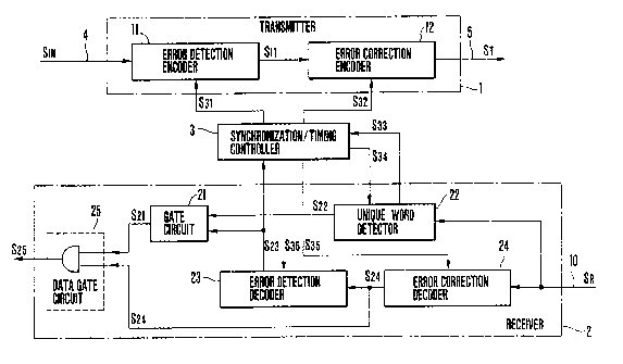
Referring to Fig. 1, the digital communication apparatus
comprises a transmitter 1, a receiver 2, and a
synchronization/timing controller 3 for controlling the operations
of the transmitter 1 and the receiver 2.
The transmitter 1 includes an error detection encoder 11
and an error correction encoder 12. The error detection encoder
11 adds an error detection check bit for detecting a code error to
, 5a
`~?, `.
13(~274
7118~-86
an information signal SIN to be transmitted, which is input
through a llne ~, in accordance with a contr~l signal S31 from the
controller 3 50 as to generate an information signal S
constituted by, e.g., a cyclic code.
5b
13~)1274
An error detector using a cyclic code is
described in detail in YAMAMOTO, "Data Communication", pp.
82 - 107.
The error correction encoder 12 receives the
information signal Sll to which the error detection check
bit is added by the error detection encoder 11. The error
correction encoder 12 performs an error correction encoding
process in accordance with a control signal S32 from the
controller 3 so as to add redundancy based on a
predetermined rule to the information signal Sll, and
transmits the resultant signal to a channel 5 as a
transmission signal ST.
The receiver 2 includes a gate circuit 21, a
unique word detector 22, an error detection decoder 23, and
an error correction decoder 24. A reception signal SR
input from another station through a transmission path 10
is input to the error correction decoder 24 and the unique
word detector 22. The error correction decoder 24 performs
an error correction decoding process of the reception
signal SR in accordance with a control signal S35 from the
controller 3 to restore a reception information signal S24
corresponding to the information signal S11 from the source
station. Then, the error correction decoder 24 transmits
the reception information signal S24 to one input of a data
gate circuit 25 and also outputs it to the error detection
decoder 23.
~ ~ ~ Z 7~
The error detection decoder 23 compares a check
bit obtained upon checking of an error in the reception
information signal S24 with the error detection check bit
added in the transmitter side to determine
coincidence/incoincidence therebetween, and outputs a code
error detection information signal S23 to the controller 3,
one input terminal of the gate circuit 21, and to the other
input of the data gate circuit 2S only when an error is not
present. With this processing, an error is detected in
units of bits.
An output S21 of the gate circuit 21 allows to
gate the reception data, i.e., the output S24 from the
error correction decoder 24 if synchronization is obtained
and an error is not detected.
The unique word detector 22 detects a unique word
in the reception signal SR in the following manner. A
unique word is constituted by a given bit pattern.
However, the bit pattern of a unique word may be changed
into various forms because of degradation in quality of
channels or thermal noise in the system. As a result, a
unique word constituted by a correct bit pattern may not be
obtained. For this reason, an allowable range is set with
respect to the number of bit errors caused in a bit pattern
in a unique word. ~ach bit of a reception signal is
compared with a corresponding bit of a correct unique word.
When the number of incoincident bits of a bit pattern falls
within the allowable range, it is determined that a unique
130~274
word is received. When the unique word detector 22 detects
a unique word, it transmits a signal S33 representing the
timing of the unique word detection and a signal S22
representing the detected unique word to the controller 3
and the other input terminal of the gate circuit 21,
respectively.
The gate circuit 21 transmits a reception signal
detection validation information signal S21 informing that
a correct unique word is detected and a code error is not
present to the device of the next stage when conditions of
the both inputs are satisfied.
The controller 3 receives the unique word
detection timing signal S33 from the unique word detector
22, and generates timing signals S31 and S32 to be
respectively supplied to the error detection encoder 11 and
the error correction encoder 12 of the transmitter 1.
The controller 3 is designed to continuously
transmit unique word detection timing information signals
S34 to the unique word detector 22 in response to the code
error detection information signal S23 from the error
detection decoder 23 even if the unique word detection
timing signal S33 from the unique word detector 22 is not
input to the controller 3.
Even if a miss-detection of a unique word is
caused and the unique word detection timing signal S33
cannot be transmitted, the unique word detector 22 keeps
the apparatus in a synchronized state as long as the unique
lZ~4
word detection timing information signals S34 are
continuously supplied.
In addition, the controller 3 supplies a timing
signal S36 for performing error detection decoding to the
error detection decoder 23.
When the device of the next stage receives the
reception signal detection validation information signal
S21 or when it receives the code error detection
information signal S23 even if the signal S21 is not
supplied, it processes the reception information signal S24
as valid.
Additionally, the conventional apparatus does not
include the error detection encoder 11, the error detection
decoder 23, and the gate circuit 21.
An operation of the circuit shown in Fig. 1 will
be described below.
In the transmitter 1, the error detection encoder
11 adds a check bit to the information signal SIN to be
transmitted. Then, the resultant signal is subjected to
error correction encoding i.n the error correction encoder
12 and is transmitted to the channel 5 as the transmission
signal ST.
In the receiver 2 for receiving signals
transmitted from another station, the unique word detector
22 detects a unique word in the reception signal SR. In
addition, the error correction decoder 24 performs error
correction decoding of the encoded signal in -the reception
~3~}12~4
signal SR. Upon reception of a demodulated signal from the
error correction decoder 24, the error detection decoder 23
determines the presence/absence of an error in the
demodulated signal on the basis of a check bit included in
the demodulated signal. According to this error detection
scheme, most errors except for certain conditions can be
detected in units of bits by utilizing, e.g., a cyclic
code.
The gate circuit, i.e., informing signal
generator 21 generates the signal S21 for informing that
detection of a reception signal is confirmed when the
unique word detector 22 detects a unique word and the error
detection decoder 23 determines the absence of an error.
With this operation, the problems of false detection of a
unique word and of degradation in error correction
performance are simultaneously solved.
Furthermore, the synchronization/timing
controller 3 basically controls the transmission/reception
timing of the apparatus of the present invention in
response to the unique word detection, and also controls
the unique word detector to allow continuous detection of
unique words. That is, the transmission/reception timing
cannot be controlled during the miss-detection period of a
unique word. In this case, however, the detection timing
position of a unique word tends to coincide with that in
the detection period. For this reason, according to the
present invention, in addition to the basic functions, the
-- 10 --
2~4
synchronization/timing controller 3 is provided with means
for controlling the unique word detector 22 so as to be
kept in the synchronized state when the error detection
decoder 23 determines the absence of an error even if a
unique word is not detected at the unique word detection
timing described above. As a result, even if a
miss-detection of a unique word is caused, the synchronized
state is held as long as the reception information signal
is correct, and hence the reception information signal can
be processed as valid. Therefore, necessary information
can be reliably obtained.
As has been described, according to the digital
communication apparatus of the present invention, since the
scheme using both the error correction and error detection
functions is employed, a false detection of a unique word
or degradation in error ccrrection performance can be
detected, thereby preventing a reception information signal
having an error from being processed as valid. In
addition, in the miss-detection period of a unique word,
since the synchronized state can be held as long as an
error is not present in a reception information signal,
necessary information can be reliably obtained.