Note: Descriptions are shown in the official language in which they were submitted.
~3q:1~3~
This invention relates to an optical information
recording and reproducing apparatus.
Fig. 1 is a block diagram showing the structure of a
first embodiment of the optical information recording and
reproducing apparatus of the present invention.
Fig. 2 shows an arrangement of various areas of an
optical disk which is preferably used in the apparatus of the
present invention.
Fig. 3 is a flow chart illustrating the steps of self-
diagnostic operation in the first embodiment shown in Fig. 1.
Fig. 4 is a block diagram showing the structure of a
second embodiment of the optical information recording and
reproducing apparatus of the present invention.
Fig. 5 is a flow chart illustrating the steps of self-
diagnostic operation in the second embodiment shown in Fig.
4.
Fig~ 6 is a block diagram showing the structure of a
prior art optical information recording and reproducing
apparatus.
Fig. 6 i5 a block diagram showing the structure of a
prior art optical information recording and reproducing
apparatus using an optical disk. Referring to Fig. 6, an
optical disk 1 is rotated by a drive motor 2. An optical
head 3 writes information on the optical disk 1 by directing
a focused laser beam onto the optical disk 1 and reads out
the recorded information by detecting a change in the laser
beam focused and reflected from the optical disk 1. A laser
drive/head amplifier circuit 4 includes a laser drive part
for driving the laser source of the optical head 3 and a head
amplifier part for detecting a focusing error signal 100, a
tracking error signal 101 and a reproduced information signal
102. An actuàtor actuating the optical head 3 is driven by a
focusing control circuit 5 to which the focusing error signal
100 is applied, 50 that the laser beam can be accurately
focused on a guide track of the optical disk lo The actuator
.. ~
~
. ~ ~
~3~32~
actuating the optical head 3 is also driven by a tracking
control circuit 6 to which the tracking error signal 101 is
applied, so that the laser beam can accurately trace the
guide track of the optical disk 1. A data
modulation/demodulation circuit 7 modulates input data 103 to
produce a data signal 104 to be recorded on the optical disk
1 and demodulates the signal 102 reproduced from the optical
disk 1 to deliver it as output data 105. A control CPU 8
controls the information recording and reproducing system of
the apparatusO
In the prior art optical information recording and
reproducing apparatus having the structure described above,
the optical head 3 converges the laser beam and directs the
focused laser beam onto a guide track of the optical disk 1
rotating at a predetermined constant high speed. A focusing
error signal 100 and a tracking error signal 101 detected by
the head amplifie.r part of the laser drive/head amplifier
circuit 4 are applied to the focusing control circuit 5 and
the tracking control circuit 6 respectively, and these
control circuits 5 and 6 drive the actuator actuating the
optical head 3 for carrying out the focusing control and
tracking control respectively, so that the focused laser beam
can be accurately directed onto the guide track of the
optical disk 1.
In the data recording mode, the data
modulation/demodulation circuit 7 modulates input data 103 to
produce a data signal 104 to be recorded on the optical disk
1.
This signal 104 applied to the laser drive/head
-- 2
3~,1
1 amplifier circuit 4 to modulate the laser beam having a
recordable intensity, and the optical head 3 directs
such a laser beam onto the optical disk 1 to record the
data.
On the other hand, in the data reproduction
mode, the laser beam, whose level is too low to record
any data, is directed from the optical head 3 onto the
optical disk 1. The laser drive/head amplifier circuit
4 receives the reflection of the focused laser beam from
the optical disk 1 to reproduce the signal 102, and
this reproduced signal 102 is demodulated in the data
modulation/demodulation circuit 7 to appear as output
data 105.
However, when the optical disk 1 in the prior
art optical information recording and reproducing
apparatus having a structure as described above is
continuously used for a long period of time and rotated
at the high rotation speed, the optical disk 1, whose
basic material is an electrical insulating resin or a
glass, is electrostatically charged, and dust floating
in air is attracted to the surface of the optical disk
1. Also, dust intruding into the apparatus attaches to
the parts including the optical disk 1 and the lens.
Because the attracted dust absorbs and scatters the
laser beam, the recording and reproducing power of the
laser beam is lowered by about several-ten percents.
As a result, a great shortage occurs in the recording
and reproducing power of the laser beam directed onto
~3~ 2~L
the recording layer deposited on the guide tracks of the
optical disk 1, and signals cannot be satisfactorily recorded
on and reproduced from the optical disk 1.
~his gives rise to a decreased amplitude of the
reproduced signal and corresponding degrada~ion of the bit
error rate. Further, because the reduced recording power of
the laser beam results in corresponding insufficient
formation of recording pits, the prior art optical
information recording and reproducing apparatus has had such
a disadvantage that the progressive deterioration of the
recording pits with time leads to a shortened useful service
life of the optical disk.
The present invention provides an optical information
recording and reproducing apparatus in which means are
provided so as to detect whether or not an optical disk or an
internal optical system of the apparatus is fouled with dust.
In accordance with the present invention there is
provided an optical information recording and reproducing
apparatus comprising recording and reproducing means for
recording and reproducing information on and from an optical
disk loaded in the apparatus; status~of-use checking means
for checking whether the loaded optical disk is new and has
not been used yet or has been used already; error detecting
means recording and reproducing test data on and from self-
diagnostic area
32~
1 of the optical disk for detecting error information fromthe reproduced test data; error information recording
means for registering, on an error managing region of the
optical disk, the error information detected when the
self-diagnostic area of the optical disk is first used;
and error comparing means for comparing the error informa-
tion detected by the error detecting means with the
initial error information reproduced from the error manag-
ing area of the optical disk.
In the optical information recording and
reproducing apparatus of the present invention, whether
an optical disk loaded in the apparatus is new and has
not heen used yet or has been used already is checked~
When the result of checlcing proves that the loaded
optical disk has not been used yet, test data is recorded
on and reproduced from the self-diagnostic area of the
optical disk,~and initial error information detected in
the reproduced test data is registered on the error
managing area of the optical disk. On the other hand,
when the result of checking proves that the loaded
optical disk has been used already, error information
detected in the test data recorded in and then reproduced
from the self-diagnostic area is compared with the
initial error information reproduced from the error
managing area. When the result of comparison proves
that the number of detected errors is more than that
detected at the beginning of the use of the optical disk,
fouling of the optical disk or the internal optical
~L3~)~3~
system is detected.
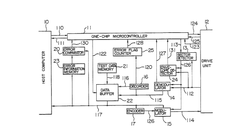
Fiq. 1 is a block diagram showing the structure of a
first embodiment of the present invention. Referring to Fig.
1, a one-chip microcontroller 11 controls the overall
apparatus in response to a device command 110 transmitted
from a host computer 10. A dxive unit 12
~3~1321
1 sends out signals 112 reproduced from sectors of an
optical disk (not shown) by an optical head (not shown).
The one-chip microcontroller 11 instructs a target
sector address 113, and a sector detection circuit 13
detects the instructed target sector address 113
among the reproduced signals 112 sent out from the drive
unit 12. An envelope detection circuit 24 detects an
envelope signal of data contained in the signal 112
reproduced from the target sector of the optical disk.
A demodulation circuit 14 demodulates the data contained
in the reproduced signal 112 and applies its output
signal 115 representing the demodulated data to a
decoder 16 and a data buffer 22. A modulation circuit
15 modulates data and applies its output signal 11~
representiny the modulated data to be recorded on the
optical disk to the drive unit 12. The decoder 16
detects and corrects errors that may be included in the
demodulated data 115, and, when errors are detected,
applies error flags 120 corresponding to the number of
detected errors to an error flag counter 25 which counts
the number of the error flags 120. An encoder 17 adds
an error detection and correction code to buffer data 117
derived from the data buffer 22. An error comparison
circuit 20 compares error information data 121 read out
from an error information memory 23 with error total-
number data 122 supplied from the one-chip microcontrol-
ler 11.
Fig. 2 shows an arrangement of various areas
~3~32~
l of an optical disk preferably used in the apparatus of
the present invention. Referring to Fig~ 2, the optical
disk includes a self-diagnostic area 32 for recording
test data to be reproduced so as to detect error informa-
tion, an error managing area 31 for registering initialerror information detected as a result of the reproduction
of the test data recorded on the self-diagnostic area 32,
and a userls area 33 for recording user's data thereon.
A flow chart o~ Fig. 3 illustrates the steps
of self-diagnostic operation carried out in the first
embodiment of the optical information recording and
reproducing apparatus having a structure as described ;
above when an optical disk having various areas as shown
in Fig. 2 is newly loaded.
Step 1
A drive interrupt signal 123 is applied to the
one-chip microcontroller 11 from the drive unit 12. In
response to this drive interrupt signal 123, the one-
chip microcontroller 11 sends out to the drive unit 12
a dxive command 124 requesting the status of disk drive
i.n the drive unit 12. In response to the drive command
124~ the drive unit 12 applies a drive status signal 125
to the one-chip microcontroller 11, and, by checking
this drive status signal 125, the one-chip microcontroller
11 detects that an optical disk is newly loaded in the
apparatus.
Step 2
As a target sector address 113, the one-chip
13~L32~
1 microcontroller 11 selects a sector address in the error
managing area 31 of the optical disk and applies such an
address signal 113 to the sector detection circuit 13.
In response to this address signal 113, the sector
detection circuit 13 detects sector address information
contained in the signal 112 reproduced from the selected
sector and applied from the drive unit 12, so as to detect
coincidence between the target sector address 113 and
the sector address information. When the target sector
is detected as a result of the coincidence detection,
the sector detection circuit 13 generates a sector
detection signal 126 so as to activate the envelope
detection circuit 24 and the demodulation circuit 14.
When the envelope detection circuit 24 detects
an envelope signal of data contained in the reproduced
signal 112, it applies an envelope detection signal
131 to the one-chip microcontroller 11. The one~chip
microcontroller 11 chec]cs as to whether or not the
envelope detection signal 131 is detected within a
rotational delay time corresponding to one sector. When
the result of checkiny proves that the envelope detection
signal 131 is not detected because the optical disk
is new and has not been used yet, the step 2 is followed
by a step 3. On the other hand, when the result of
checking proves that the optical disk has been used
already, the step 2 is followed by a step 7.
Step 3
~s the target sector address 113, the one-chip
13~ 32 !L
1 microcontroller 11 selects a sector address in the self-
diagnostic area 32 of the optical disk and applies such
an address signal 113 to the sector detection circuit 13.
In response to the address signal 113, the sector detec-
tion circuit 13 detects sector address information con-
tained in the signal 112 reproduced from the selected
sector and applied from the drive unit 12, so as to
detect coincidence between the target sector address 113
and the sector address information. When the target
sector is detected as a result of the coincidence detec-
tion, the sector detection circuit 13 generates the
sector detection signal 126 so as to activate the modula-
tion circuit 15.
First, test data 118 read out from a test
data memory 21 is supplied to the data buffer 22 to
appear as buffer data 117 rom the data buffer 22. The
encoder 17 adds an error detection and correction code
to the buffer data 117 to provide coded data 129 which
is supplied to the modulation circuit 15. The modulation
circuit 15 modulates the coded data 129 to produce a
signal 114 to be recorded, and this signal 114 is applied
to the drive unit 12 to be recorded on the self-diagnostic
area 32 of the optical disk.
The one-chip microcontroller 11 selects a
sector address in the self-diagnostic area of the
optical disk as the target sector address 113 again and
applies such an address signal 113 to the sector detec-
tion circuit 13. The sector detection circuit 13 detects
~ O -
L32~
1 sector address information contained in the signal 112
reproduced from the selected sector and applied from the
drive unit 12, so as to detect coincidence between the
target sector address 113 and the sector address informa-
tion. When the target sector is detected as a result ofthe coincidence detection, the sector detection circuit
13 generates the sector detection signal 126 so as to
activate the demodulation circuit 14.
The demodulation circuit 14 demodulates the
reproduced signal 112 applied from the drive unit 12
while discriminating data contained in the reproduced
signal 112 and supplies the demodulated data 115 to the
decoder 16.
Step 4
The decoder 16 detects and corrects errors
inclucled in the demodulated data 115. That is, the
decoder 16 carries out error correction by grouping
errors into an error syndrome, calculating the number of
error symbols for each individual code word, and finding
error symbol locations and error symbol values. For
the purpose of this manner of error detection and correc-
tion, a BC~ code i5 used. Such a method of error detec-
tion and correction by the use of the BCH code is
described in detail in chapter 9 of a book entitled
"ERROR-CORRECTING CODES", SECOND EDITION (W.Wesley Peterson
and E.J~ Weldon Jr., The MIT PRESS, CAMBRIDGE MASSACHU-
SETTS AND LONDON, ENGL~D, 1975).
In the course of error detection and correction,
~3~32~L
1 the decoder 16 detects the number of error symbols fora given code word and sends out an error flag 120 represen-
ting the number of error symbols to the error flag
counter 25. The error flag counter 25 sends out the
count of the error flags 120 representing the same number
to the one-chip microcontroller 11 as error data 128. In
the one-chip microcontroller 11, the count of the error
flags 120 representing the same number is multiplied by
the number of the error symbols represented by that
error flag 120 to calculate the total number of the
error symbols.
Suppose, for example, that the decoder 16 can
detect a maximum of three error symbols for each indivi-
dual code word, and there are Ll, L2 and L3 code words
having one, two and three error symbols respect;.vely.
When the decoder 17 detects one, two or three error
symbols i.n each individual code word, an error flag 120
indicating one, two or three errors is sent out from the
decoder 16 to the error flag counter 25. Thus, the one-
chip microcontroller 11 receiving the error data 128from the error flag counter 25 is informed that there
are Ll, L2 and L3 code words having one error symbol,
two error symbols and three error symbols respectively.
The one-chip microcontroller 11 calculates the total
number of error symbols according to the following
equation:
(Total number of error sumbols) = Llx 1 + L2x 2 ~ L3x 3
- 12 -
~3[)~32~L
1 Step 5
When the one-chip microcontroller 11 finds that
the total number of error symbols is equal to or larger
than a predetermined reference value N, it decides that
the optical disk or the internal optical system of the
apparatus is fouled to such an extent that the optical
information recording and reproducing function cannot be
normally performed. In this case, the step 5 is followed
by a step 9.
lo Step 6
When the total number of error symbols is
smaller than the predetermined reference value N, error
total-number data 122 obtained by formatting the total
number of erro.r symbols is sent out to the data buffer
22 from the one-chip microcontroller 11.
Further, the one-chip microcontroller 11
selects a sector address in the error managing area 31
of the optical disk as the target sector address 113
and applies such an address signal 113 to the sector
detection circuit 13. The sector detection circuit 13
detects sector address information contained in the
signal 112 reproduced from the selected sector and
appli.ed from the drive unit 12, so as to detect coincid-
ence between the target sector address and the sector
address information. When the target sector is detected
as a result of the coincidence detection, the sector
detection circuit 25 generates the sector detection
signal 126 for activating the modulation circuit 15.
- 13 -
~3~32:~
1 The error total-number data 122 supplied to the
data buffer 22 from the one-chip microcontroller 11
appears as buffer data 117 from the data buffer 22, and
the encoder 17 adds the error detection and correction
code to the buffer data 117 to provide coded data 129
which is supplied to the modulation circuit 15. The
modulation circuit 15 modulates the coded data 129 to
: produce a signal 114 to be recorded, and this signal 114
is applied to the drive unit 12. Thus, the total number
: 10 of initial error symbols detected on the self-diagnostic
area 32 is now recorded on the error managing area 31
of the optical disk, thereby completing execution of the
self-diagnostic operatlon.
Step 7
This step is executed when the result of
checking in the step 2 proves that the optical disk is
not new and has been used already.
The demodulation circuit 14 demodulates the
reproduced signal 112 applied from the drive unit 12
while discriminating data contained in the reproduced
signal 112 and supplies the demodulated data 115 to the
decoder 16. The decoder 16 detects and corrects errors
included in the demodulated data 115 and supplies repro-
duced data 116 to the data buffer 220 Further, the
data of the total number of initial error symbols
detected on the self-diagnostic area 32 of the optical
disk by recording and reproducing test data thereon and
derived from the data buffer 22 as buffer data 117 is
- 14 -
~3~L32~
1 stored in the error information memory 23 under control
of the one-chip microcontroller ll.
Step 8
The error total-number data 122 obtained by
formatting the total number of error symbols is sent out
to the data buffer 22 from the one-chip microcontroller
11 .
The error comparison circuit 20 compares the
buffer data 117 derived from the data buffer 22 with the
error information data 121 read out from the error
information memory 23 to calculate the ratio between the
data 117 and 121. When the calculated ratio is equal to
or larger than a predetermined reference value M, the
optical disk or the internal optical system of the appa-
ratus is fouled, and the optical information recording andreproducing function cannot be normally performed~ A
siynal 130 indicating the impossibility of normally
performing the recordin~ and reproducing function is
applied from the error comparison circuit 20 to the one-
chip microcontroller ll. On the other hand, when theratio described above is smaller than the predetermined
reference value M, the optical information recording and
reproducing function is normal, and the execution of the
self-diagnostic operation is completed.
Step g
When, in response to the device command 110
transmitted from the host computer 10, the one-chip
microcontroller 11 applies sense information 111 to the
~ 15 -
~3~321
1 host computer 10 to inform that the optical disk or the
internal optical system is fouled, and the optical
information recording and reproducing function cannot be
normally performed, the execution of the self-diagnostic
operation is completed.
In the step 2, the envelope detection circuit
24 can detect the envelope signal by detecting that a
retriggerable monostable multivibrator, to which the
binary reproduced signal 112 is applied as an input,
generates an output which becomes continuously active by
a number of times which is a predetermined multiple of
the tlme constant T of the multivibrator. The fact that
the output of the multivibrator becomes continuously
active can be confirmed by detecting the fact that the
output becomes active by k times as a result of sampling
the output by n times. Further, although whether or not
the optical disk has been used already is decided on
the basis of the envelope detection signal 131, it can
be decided on the basis of a busy signal 127 generated
from the demodulation circuit 1~ when the demodulation
circuit 14 is activated by the signal 126 produced on the
basis of the signal 112 reproduced from the recorded
sector.
Further, those skilled in the art will readily
understand that the host computer 11 can perform the
functions of the error flag counter 25 and error compar-
ison circuit 20 employed in the first embodiment.
It will be seen from the above description
- 16 -
32~.
1 that, in the first embodiment of the optical information
recording and reproducing apparatus of the present
invention, the error flag countex 25 counts the number
of error flags 120 detected by the decoder 16 when an
optical disk which is new and has not been used yet
starts to be used for optical information recording and
reproduction and also during the use of the optical disk
for the sarne purpose. The total number of the error
symbols counted in the latter case is compared in the
error comparison circuit 20 with that counted in the
former case. When an increase in the data errors is
detected as a result of the error flag comparison in
the error comparison circuit 20, the one-chip microcon-
troller 11 can detect that the optical information
recording and reproducing function cannot be normally
performed due to r Eor example, fouling of the optical
disk or the internal optical system of the apparatus.
Fig. 4 is a bloc~ diagram showing the struc-
ture of a second embodiment of the optical information
recording and reproducing apparatus of the present
invention. In Fig. 4, the reference numerals 10 to 17,
24, llO to 118 and 121 to 131 designate the same parts
and signals as those used in the first embodiment shown
in Fig. 1. Referring to Fig. 4, an error bit detection
circuit 18 compares buffer data 117 derived from the
data buffer 22 with test data 118 read out from the
test data memory 21 to detect error information. An
error bit counter 19 counts error bits represented by
- 17 -
32~.
1 an output signal 119 of the error bit detection circuit
18.
The arrangement of various areas of an
optical disk preferably used in the second embodiment
of the present invention is the same as that of the
optical disk shown in Fig~ 2.
The self-diagnostic operation of the second
embodiment of the optical information recording and
reproducing apparatus having the illustrated structure,
when an optical disk is newly loaded, will be described
with reference to a flow chart of Fig. 5.
In the following description, operations in
steps 1, 2 and 9 in Fig. 5 are the same as those in
the steps 1, 2 and 9 respectively in Fig. 3, and opera-
tions in steps 12 to 15 in Fig. 5 are also the same asthose in the steps 5 to 8 respectively in Fig. 3, except
that the term "error symbol" is replaced by the term
"error bit". Therefore, those steps need not be
described again, and operations in steps 10 and 11 will
only be described herein.
Step 10
As in the case of the step 3/ test data is
recorded on and reproduced from the self-diagnostic
area 32 of the optical disk. However, the step 10
differs from the step 3 in that, buffer data 117 is
directly supplied to the modulation circuit 15 without
being passed through the encoder 17, whereas coded data
12~ provided by adding the error detection and correction
- i8 -
~31)~32~l
1 code to test data 118 by the encoder 17 is supplied to
the modulation circuit 15 in the step 3.
Step 11
Error information is detected by the error bit
detection circui.t 18. First, the demodulation circuit 14
demodulates a reproduced signal 112 applied from the
drive unit 12 while discriminating data contained in the
signal 112, and the demodulated data 115 from the
demodulation circuit 14 is directly supplied to the data
buffer 22 without being passed through the decoder 16.
In the error bit detection circuit 18, the buffer data
117 derived from the data buffer 22 is compared bit-to-
bit with the test data 118 read out from the test data
memory 21, and, each time non-coincidence therebetween
is detected, an error bit detection signal 119 is applied
to the error bit counter 19. The data representing the
number of error bit detection signals 119 counted by the
error bit counter 19 is supplied to the one-chip micro-
controller 11 as error data 128. The value of this
error data 128 repxesents the total number of occurred
error bits,
The error bit detecting operation of the error
bit detection circuit 18 and the error bit counting
operation of the error bit counter 19 in the second
embodiment can be easily realized by means of software
prepared in the one-chip microcontroller 11 to dispense
with the provision of such hardware parts. Also, the
operations of the error bit detection circuit 18, error
_ 19 _
l bit counter 19 and error comparison circuit 20 can be
easily done by the host computer 10.
Further, the operation of the error ccmparison
circuit 20 in each of the first and second embodiments
may also be easily realized by means of software prepared
in the one-chip microcontroller 11. Further, although
the test data 118 recorded on the optical disk so as to
obtain error information is stored in the test data
memory 21, the test data 118 may be supplied from the
host computer 10.
In the second embodiment of the optical informa-
tion recording and reproducing apparatus having the
features described above, the error bit detection circuit
18 detects error bits included in demodulated data not
subjected to error correction, and the error bit counter
l9 counts the total number of such error bits. The total
number of error bits counted when the optical disk,
which is new and has not been used yet, starts to be used
for the optical information recording and reproducing
purpose and that counted during the use of the optical
disk for the same purpose are compared in the error
comparison circuit 20. When an increase in the data
errors is detected as a result of the error bit
comparison in the error comparison circuit 20, the one-
chip microcontroller 11 can detect that the opticalinformation recording and reproducing function cannot be
normally performed due to, for example, fou~ing of the
optical disk or the internal optical system of the
- 20 -
- - 13~)~32~L
apparatus,
In the aforementioned embodiments of the pre-
sent invention, the self-diagnostic operation for
detecting fouling of an optical disk or the internal
optical system of the apparatus starts when the optical
disk is lead in position in the apparatus. However, this
self-diagnostic operation may start when the power
supply for the apparatus is turned on or when a device
command 110 requesting diagnosis is transmitted from the
host computer 10. Therefore, the self-diagnostic
operation is also carried out even in an optical informa-
tion recording and reproducing apparatus of the type in
which an optical disk is completely enclosed.
It will be understood from the foregoing
detailed description that, the present invention provides
an optical informat.ion recording and reproducing
apparatus in which fouling of an optical disk or its
internal optical system is detected by comparing the
total number of errors detected when the optical disk,
which is new and has not been used yet, starts to be used
for optical information recording and reproduction with
that detected during the use of the optical disk,
thereby detecting an increase in errors included in
recorded and reproduced test data. Therefore, fouling
of the optical disk and the internal optical system of
the apparatus can be detected with high reliability, ar.d
the apparauts has great practical effects.
- 21 -