Language selection

Search

Patent 1301370 Summary

Third-party information liability

Some of the information on this Web page has been provided by external sources. The Government of Canada is not responsible for the accuracy, reliability or currency of the information supplied by external sources. Users wishing to rely upon this information should consult directly with the source of the information. Content provided by external sources is not subject to official languages, privacy and accessibility requirements.

Claims and Abstract availability

Any discrepancies in the text and image of the Claims and Abstract are due to differing posting times. Text of the Claims and Abstract are posted:

  • At the time the application is open to public inspection;
  • At the time of issue of the patent (grant).
(12) Patent: (11) CA 1301370
(21) Application Number: 597203
(54) English Title: INTEGRATED CIRCUIT PACKAGE USING PLASTIC ENCAPSULANT
(54) French Title: BOITIER DE CIRCUIT INTEGRE UTILISANT UN ENCAPSULANT DE PLASTIQUE
Status: Deemed expired
Bibliographic Data
(52) Canadian Patent Classification (CPC):
  • 356/143
(51) International Patent Classification (IPC):
  • H01L 23/29 (2006.01)
  • H01L 23/057 (2006.01)
  • H01L 23/24 (2006.01)
(72) Inventors :
  • COHN, CHARLES (United States of America)
(73) Owners :
  • AMERICAN TELEPHONE AND TELEGRAPH COMPANY (United States of America)
(71) Applicants :
(74) Agent: KIRBY EADES GALE BAKER
(74) Associate agent:
(45) Issued: 1992-05-19
(22) Filed Date: 1989-04-19
Availability of licence: N/A
(25) Language of filing: English

Patent Cooperation Treaty (PCT): No

(30) Application Priority Data:
Application No. Country/Territory Date
184,214 United States of America 1988-04-21

Abstracts

English Abstract


-5-
Abstract
An integrated circuit package uses an encapsulant frame which
prevents the encapsulant used to seal the integrated circuit chip from the ambient
atmosphere from flowing to unwanted areas and to permit the encapsulant to be
deposited with a controllable depth.


Claims

Note: Claims are shown in the official language in which they were submitted.


- 4 -
Claims:
1. An integrated circuit package comprising a mounting plate having a
metallic pattern on at least one major surface and a plurality of recesses;
an integrated circuit chip mounted on said plate;
a plurality of electrical leads from said chip to said metallic pattern on
said mounting plate;
an encapsulant frame encircling said chip and having a plurality of
retention pins in said recesses; and
an encapsulant disposed within said encapsulant frame sealing said
chip from the ambient atmosphere.

2. A package as recited in claim 1 in which said mounting plate
comprises a printed circuit board.

3. A package as recited in claim 1 in which said mounting plate
comprises a ceramic substrate.

4. A package as recited in claim 1 in which said encapsulant has a
surface approximately level with the surface of said frame.


Description

Note: Descriptions are shown in the official language in which they were submitted.


3~


INTEG~ATED CIRCUIT PACKAGE USING PLASTIC ENCAPSULANT
Techllical Field
This invention relates to integrated circuit packages using an encapsulant to
protect the integrated circuit chip.
Back~round of the Invention
S Although most attention in integrated circuit manufacturing is presently
focused on the steps required to fabricate an integrated circuit chip, the assembly of various
components, including the chip, into a package is a commercially significant process. A~ter
fabrication of the integrated circuit chip has been completed, the chip must be mounted on an
underlying material so that it can be e~pediently handled as well as electrically contacted. One
technique mounts the chip directly on a printed circuit board. A printed circuit board typically
is a dielectric material having a metallic pattern on at least one major surface with selected
portions of the pattern being electrically contacted to appropriate portions of the chip.
Another technique mounts the chip within a plastic package cavity which in tu~n is mounted
on, e.g., a printed circuit mother board. However, both mounting techniques typically use
some approach to protect the chip t`rom adverse effects, i.e., to seal the chip from the ambient
atmosphere. A ceramic could also be used as the underlying material.
One such approach uses a glob of epoxy over the chip. Another approach uses
a plastic cap which is cemented over the chip. Both approaches, ur~t`ortunately, have
drawbacks. For example, the disadvantages of the epoxy glob include a tendency of the epoxy
to spread irregularly over the surface surrounding the chip, i.e., the epoxy tlows and neither
the direction nor extent of the t~ow can be precisely controlled. ~dditionally, as will be readily
appreciated, the thickness of the epoxy over the chip cannot be precisely controlled. The use
of a plastic cap avoids both of these drawbacks but is, unfortunately, costlier to implement
than is the epoxy glob due to the nature of the assembly step required. Additionally, the cap
should be leak tested after it is cemented in place to insure that deleterious contaminants will
not enter the cap and damage the chip because there is not a tight seal between the cap and
the underlying material.
Summar~ of the Inv~ntion
In accordance with one aspect of the invention there is provided an integrated
circuit package comprising a mounting plate having a metallic pattern on at least one major
surface and a plurality of recesses; an integrated circuit chip mounted on said plate; a plurality
of electrical leads from said chip to said metallic pattern on said mounting plate; an
encapsulant frame encircling said chip and having a plurality of retention pins in said recesses;


and an encapsulant disposed within said encapsulant frame sealing said chip from the ambient
atmosphere.
Brief Description of the Drawin~
FIG. 1 is a sectional view of an integrated circuit package according to this
5 invention; and
~ :;IG. 2 is a perspective view of an exemplary plastic frame according to this
invention.
Detaile(l Description
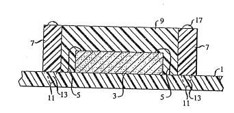
An exemplary package is shown in the sectional view in F~G. 1. For reasons of
10 clarity, the elements of the package are not drawn to scale. Depicted are a mounting plate 1;
an integrated circuit chip ~; a plurality of electrical leads S between said rnounting plate and
said chip; and an encapsulant frame 7. Within the encapsulant frame is an encapsulant 9.
The rnounting plate has a plurality of recesses 11 and the frame has a plurality of retention
pins ~3 which mate with said recesses. Typical mounting plates are printed circuit boards or
15 ceramic substrates.
After attaching and wire bonding the chip to, e.g., a printed circuit board using
well known techniques, the encapsulant t`rame is mounted on the printed circuit board using
techniques well known to those skilled in the art and the encapsulant, e.g., liquid epoxy, is
dispensed over the cllip until it is approximately level with the top of the frame or until the
20 chip has been appropriately sealed from the atmosphere.
Accurate positioning of the encapsulant frame on the printed circuit board is
facilitated by the plurality of recesses on lhe board adapted to receive, i.e., mate with, the
plurality of retention pins on the encapsulant frame.
On the side of the frame opposed to the retention pins, there will desirably be
25 a plurality of bumps which allow for an air gap between the encapsulant and the mother board
on which the package is mounted. The package is mounted with the chip and the encapsulant
surface facing the board. The air gap, because of the spacing caused by the bumps, facilitates
cleaning underneath the package if that becomes necessary.
The material used for the frame is not critical and one skilled in the art will
30 readily be able to select an appropriate material. An exemplary material is a high temperature
plastic such as polyphenylene sulfide.

~V~3~
- 3 -
FIG~ 2 is a perspective view of a plastic frame according ~v .~
invention showing the plurality of retention pins 13 and a plurality of sphe~ical
bumps 17 depicted.

Representative Drawing
A single figure which represents the drawing illustrating the invention.
Administrative Status

For a clearer understanding of the status of the application/patent presented on this page, the site Disclaimer , as well as the definitions for Patent , Administrative Status , Maintenance Fee  and Payment History  should be consulted.

Administrative Status

Title Date
Forecasted Issue Date 1992-05-19
(22) Filed 1989-04-19
(45) Issued 1992-05-19
Deemed Expired 2002-05-21

Abandonment History

There is no abandonment history.

Payment History

Fee Type Anniversary Year Due Date Amount Paid Paid Date
Application Fee $0.00 1989-04-19
Registration of a document - section 124 $0.00 1989-08-30
Maintenance Fee - Patent - Old Act 2 1994-05-19 $100.00 1994-03-24
Maintenance Fee - Patent - Old Act 3 1995-05-19 $100.00 1995-04-25
Maintenance Fee - Patent - Old Act 4 1996-05-20 $100.00 1996-04-04
Maintenance Fee - Patent - Old Act 5 1997-05-20 $150.00 1997-04-07
Maintenance Fee - Patent - Old Act 6 1998-05-19 $150.00 1998-03-25
Maintenance Fee - Patent - Old Act 7 1999-05-19 $150.00 1999-03-19
Maintenance Fee - Patent - Old Act 8 2000-05-19 $150.00 2000-03-20
Owners on Record

Note: Records showing the ownership history in alphabetical order.

Current Owners on Record
AMERICAN TELEPHONE AND TELEGRAPH COMPANY
Past Owners on Record
COHN, CHARLES
Past Owners that do not appear in the "Owners on Record" listing will appear in other documentation within the application.
Documents

To view selected files, please enter reCAPTCHA code :


To view images, click a link in the Document Description column. To download the documents, select one or more checkboxes in the first column and then click the "Download Selected in PDF format (Zip Archive)" or the "Download Selected as Single PDF" button.

List of published and non-published patent-specific documents on the CPD .

If you have any difficulty accessing content, you can call the Client Service Centre at 1-866-997-1936 or send them an e-mail at CIPO Client Service Centre.


Document
Description 
Date
(yyyy-mm-dd) 
Number of pages   Size of Image (KB) 
Representative Drawing 2000-12-18 1 14
Drawings 1993-10-30 1 26
Claims 1993-10-30 1 21
Abstract 1993-10-30 1 7
Cover Page 1993-10-30 1 14
Description 1993-10-30 3 114
Fees 1997-04-07 1 74
Fees 1996-04-04 1 77
Fees 1995-04-25 1 59
Fees 1994-03-24 1 41