Note: Descriptions are shown in the official language in which they were submitted.
13016~8
FIELD OF THE INVENTION
2 The present invention relates to a low amplitude wood composite
3 board panel having an undulating, or wave-like, configuration.
4 BACKGROUND OF THE INVENTION
Typically, a wafer board panel comprises layers of wood
6 flakes or wafers formed into a composite structure using a
7 resinous binder. ~he preparation of wafer board panels is
8 complex, but broadly consists of two principal stages. The first
g stage comprises the preparation of the wafers and admixing
thereof with the binder to form a loose layer or mat; the second
11 stages involves subsequent compression and heating of the mat to
12 cure the binder and form the consolidated panel.
13 At present, wafer board is usually manufactured in the
14 form of planar or flat sheets. Wafer board is a recognized
structural panel, finding wide application in the construction
16 industry, particularly as a plywood substitute in residential
17 construction.
18 Improvement in performance characteristics of flat
19 wafer board panels has been attained by optimisation of such
parameters as wafer orientation, wafer geometry, resin selection
21 and content, and the like.
22 By wafer orientation is meant orientation through a
23 degree of rotation which may range from the longitudinal to the
24 transverse directions. Furthermore the orientation may take
place in a layered or non-layered manner. Stated otherwise, the
26 outer faces of the board only may contain orientated wafers
27 whereas the core may contain wafers in random orientation.
28 Alternatively, the orientation may be such that all the layers
130~618
1 throughout the board are consistently aligned in one direction.
2 After exhaustive optimization studies of planar wafer
3 board panels it was postulated that its flexural strength
4 characteristics could ~e improved if a corrugated configuration
was imparted thereto. The fundamental concept of corrugat~ng
6 materials to thereby improve the structural properties is not a
7 novel one. Indeed, corrugated wafer board panels per se have
8 previously been manufactured in the industry. However, ~he wafer
g board panels prepared by these prior art techniques do not have
the desired structural strength properties because they do not
11 have a substantially uniform density.
12 Until recently, wafer board panels were manufactured in
13 the form of planar or flat sheets. However, as disclosed in U.S.
14 Patent 4,616,991, the present applicant has developed an
apparatus and process for the manufacture of panels having a
16 wave-like or corrugated configurat-ion. Such waveboard panels have
17 improved structural strength properties, relative to planar
18 panels.
19 This prior patented apparatus involved a pair of
opposed, spaced-apart, upper and lower platens. Each platen was
21 formed of adjacent lengths of chain-like links. When the lengths
22 were pushed inwardly from the side, they would shift from a
23 planar to an undulating corrugated form.
24 The process steps involved:
- distributing a mat of loose wood wafers between
26 the upper and lower platen surfaces while they are
27 maintained in the planar configuration;
28 biasing the platens together to pre-compress the
29 mat, and thereby substantially fixing the wafers
130~618
1 together to limit their further relative movement;
2 - converting the two platen surfaces, still in
3 pressing association with the mat, from the planar
4 to the corrugated configuration; and
- then applying additional pressure and heat for a
6 sufficient time to cure the binder and produce a
7 corrugated waveboard panel.
8 The main advantage inherent in the patented process was
g that the panel product so formed was characterized by a
substantially uniform density. This was achieved because the
11 wafers were fixed by the pre-compression step and because the mat
12 was not significantly stretched or elongated during the
13 conversion from the planar to the corrugated configuration.
14 It will be also noted that the product formed using the
particular mechanical assembly described hereabove has a
16 generally sinusoidal configuration. The peaks and troughs of the
17 panel have a generally rounded profile. The amplitude of the
18 waves of such panels would range from 12mm to 50mm. By amplitude
19 is meant the distance between the centroid (or zero lineJ and the
wave crest. Wave length is defined as the distance between two
21 adjacent wave crests. By low amplitude waveboard as defined
22 herein is meant waveboard having an amplitude substantially equal
23 to the board thickness in the ranges defined hereinafter.
24 Whilst the above-described apparatus provides a useful
product it will be readily appreciated by one skilled in the art
26 that the cost of manufacture of such corrugating platens is
27 significant.
28 In summary, therefore, prior to the development of the
29 present invention, it had been appreciated that by having a high
~301618
1 amplitude waveboard prepared using the above-described platen
2 assembly a marked improvement in mechanical performance
3 characteristics was obtained. However, what had not been
4 realised was that providing even a minor degree, or very low
amplitude of corrugation to the board would result in mar~edly
6 improved properties as compared to a planar panel.
7 SUNMARY OF l'HE INVENTION
8 In accordance with the present invention a low
g amplitude waveboard panel having improved bending strength and
bending stiffness properties is provided. More specifically, in
11 order to obtain this improvement the wave amplitude must be
12 substantially equal to or less than the thickness of said board.
13 Preferably, the amplitude of said waves would range from between
14 about 1/8" to about l".
Preferably, the panels would be prepared from wood
16 wafers in admixture with a binder.
17 Additionally, it has been observed that by
18 substantially orientating or aligning the entire content of the
19 wafers in a direction generally parallel to the profile of the
wave-front it is possible to greatly increase the bending
21 stiffness of the waveboard. Even partial alignment of the wafers
22 has been found to increase the performance properties of the
23 waveboard.
24 In a second aspect of the invention, it has been found
that the low amplitude waveboard may be manufactured by the
26 simple expedient of mounting suitably spaced elongate rectangular
27 iron bars or the like, on both the upper and lower press platens.
13016i8
1 Thus, when the press is in the closed position the space between
2 the working face of the iron bar and the surface of the press
3 platen defines the amplitude of the waveboard.
4 It is to be noted, however, that when utilizing such an
assembly, the mat of wafers plus binder in admixture must be
6 placed between a pair of flexible screen members before
7 positioning between the platens. As a result of this provision,
8 it is effectively possible to avoid the displacement or
g ~stretching~' of the wafers in the zone between corners of opposed
upper and lower bars, which would otherwise take place.
11 The advantages arising from the present invention thus
12 involve a product which can be relatively simply and
13 inexpensively manufactured yet which exhibits marked improvement
14 in performance characteristics.
Broadly stated the invention comprises a board formed
16 of a composite material said board having at least one half wave
17 formed therein wherein the amplitude of the wave is substantially
18 equal to or less than the thickness of said board.
19 DESCRIPTION OF THE DRAWINGS
Figure 1 is a comparative illustration of the profiles
21 of sinusoidal corrugated waveboard, low amplitude waveboard and
22 planar waferboard to accompany the panel property values thereof
23 which are detailed in Table I herein.
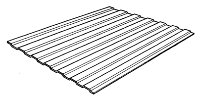
24 Figure 2 is a perspective view of a finished waveboard
panel.
26 Figure 3 is a schematic illustrating the press steps
27 employed in the process of the present invention.
28 Figure 4 is a side-sectional detailing the dimensions
~30~6~8
1 of the board.
2 DESCRIPTION OF THE PREFERRED EM~ODIMENT
3~aving reference to the accompanying drawings there is
4shown at 1 the press system utilized to manufacture the low
5amplitude waveboard.
6More specifically, upper and lower platens 2a and 2b
7respectively, each include a base plate 3.
8A plurality of spaced apart, parallel longitudinally
9extending rectangular bars 4 are affixed to the working surface
10of the base plates 3.
11In order to obtain a low amplitude waveboard of
12thickness "A" and wave-length "B" the platens would be arranged
13as shown in the figures.
14The horizontal platen assemblies are arranged in spaced
15apart opposed relationship as shown in Figure 3. Conventional
16press members (not shown) are connected to the platen assemblies
172, for biasing the latter together in a vertical direction and
18applying pressure thereto.
19As would be evident to one skilled in the art, the
20waveboard may be manufactured form a variety of suitab~e
21materials, exemplary of which would be wood composite materials.
22The process for producing the low amplitude waveboard
23from wood wafers was as follows:
24The furnish could be prepared using various wood
25species. Aspen logs approximately 8" length and 6 - 14" in
26diameter were used. The logs were cleaned, debarked waferized
27and screened in accordance with conventional methods. The strand
28or wafer length could range from 2~ mm to 300 mm, but preferably
13016~8
1 would be 50 mm to 100 mm for the best results. The thickness of
2 the wafers was about 0.75 mm. The width of the strands may range
3 up to 50 mm.
4 The moisture content of the furnish was reduced from
the green state to about 5% using commercial dryers. The wafers
6 were screened following drying.
7 At 5~ moisture content, the furnish was blended with
8 about 2~ to 3% by weight of powdered phenol formaldehyde resin
9 and 1~ by weight wax in a drum blender. Wax was utilized to
improve the moisture resistance of the panel. ~esin was used as
11 a binder for the wafers.
12 The wafers and wax/resin or binder, in admixture were
13 arranged loosely between two flexible screens to form the mat.
14 Alternatively and advantageously the wafers may be orientated
(using methods conventional in the art) parallel to the profile
16 of the wave-front. By arranging the wafers in this manner, I
17 have determined that the bending stiffness of the panel may be
18 approximately doubled, as shown in Table III herebelow.
19 The quantity of wafers and resin used was sufficient to
produce a board having a density of 600 - 800 kg/m3.
21 In order to avoid having areas of lower density in the
22 panel in the sone marked "Z", I have determined that it is
23 essential to uniformly spread the mat between flexible screens
24 before placing it between the platens. Suitable screens could be
manufactured from such exemplary materials as high tension carbon
26 steel mesh wire screen type #163 supplied by Gerald Daniel & Co.
27 Inc., N.Y.
28 In the press, the mat was subjected simultaneously to
29 high temperature, which cured the resin and to high pressure
~3016~8
l which compressed the mat to its specified thickness. The platen
2 temperature was maintained at 205c.
3 Table I given herebelow provides a comparison of the
4 panel properties of the sinusoidal corrugated waferboard, low
amplitude and planar waferboard illustrated in Figure 1. The low
6 amplitude panels were made using the malelfemale press platens
7 illustrated in Figure 3.
8 TABLE I
g (ControlJ Low
Flat Amplitude
11 Panel Propertieswaferboardwaferboard
12 Panel density (kg/m3)665 643
13 Unit panel mass rkg/m2) 7.7 7.6
14 Wavelength (mm) -- 114
Panel depth (mmJ 11.6 25
16 Skin thickness (mmJ 11.6 11.6
17 MC (~) 3.6 3.9
18 Unit max. moment
19 (NmmlmmJ 587 943
Bending stiffness
21 Unit El (Nmm2/mm) 724,000 2,460,000
22 All the panels were prepared in the above example using
23 random oriented flakes. All panels were manufactured using 75 mm
24 long aspen flakes of 0.75 mm thickness. The weight of powdered
phenolic resin was 3%.
26 Table II given herebelow shows the panel properties of
130~618
1 two different density low amplitude waveboard panels compared to
2 flat waferboard. The panels were prepared using the press
3 platens and flexible screen system described herein. The wafer
4 orientation was random.
TABLE II
6 (ControlJ Low Low
7 Flat Amplitude Amplitude
8 Panel Properties waferboard waferboard waferboard
g Normal High Normal
Density Density Density
11 Panel density (kg/m3J665 801 661
12 Unit panel mass (kg/m2J 4.1 5.5 4.0
13 Wavelength (mmJ -- 89 89
14 Panel Depth (mmJ 6.2 12.7 12.7
Skin Thickness (mm) 6.2 6.8 6.1
16 MC (%) 3.3 3.6 4.1
17 Unit max. moment (M maxJ
18 (Load Capacity) (Nmm/mm) 168 368 247
19 Bending stiffness
Unit E1 (Nmm2/mm) 96,600 504,000 322,000
21 In Table III herebelow there is provided a comparison
22 between low amplitude waveboard having strongly orientated wafers
23 versus low amplitude waveboard having randomly orientated wafers.
24 By "strongly" orientated wafers is meant that a major portion of
the wafers, throughout its thickness, are orientated in one
26 direction, specifically parallel to the major axis of the wave
27 front.
1~10~618
TABLE III
2 Low Arnplitude (Control)
3 Corrugated Flat
4 Panel PropertiesWaferboard Waferboard
Wafer Orientation*StrongMedium Random Random
6 Relative to Test
7 Span
8 Panel Density (kg/m3J 644 660 638 642
g Unit Panel Mass (Kg/m2) 4.1 4.1 4.0 4.2
~avelength (mmJ 89 89 89 __
11 Panel Depth (mm) 13.1 12.8 12.8 6.5
12 Skin Thickness (mm) 6.4 6.2 6.3 6.5
13 MC (%) 3.9 3.6 4.1 3.4
14 Unit Max. Moment
(load Capacity) (Nmm/mm)
16 (M max) 377 346 221 147
17 Bending Stiffness
18 (Nmm2/mm) 641,000 496,000 326,000 94,000
19 Replications (-) 8 4 8 8
*The wafer orientation for each panel was the same in face and
21 core layers unlike that for commercial oriented flat waferboard.