Note: Descriptions are shown in the official language in which they were submitted.
13~)1826
SOLID STATE PROTECTOR UNIT
Technical Field
This invention relates to protectors for use
in telephone central offices or other locations and, in
5 particular, to solid state protectors.
Background of the Invention
Protecting telecommunications equipment in
telephone central offices or other locations against
sneak currents and voltage surges is well known.
10 Traditional protectors include carbon blocks and gas
tubes. These protectors, however, have a wide spread in
voltage breakdown levels and large variability with
surge rise time. The life, furthermore, of a carbon
block is limi ted. Gas tubes and carbon blocks protect
15 either tip conductor or ring conductor but not balanced
protection on both.
The problems with gas tubes and carbon blocks
have been solved by using solid state devices. Solid
state protectors have instantaneous response for all
20 surges, longer life and provides balanced protection on
both tip and ring for high voltages on either tip or
ring. An example of a circuit for balanced protection
is shown in U. S. Patent Number 4,408,248 issued
October 4, 1983 to R. M. Bulley et al. An example of a
25 solid state protector circuit is disclosed in U. S.
Patent Number 4,408,2g8 issued October 4, 1983 to
~. M. Bulley et al. An example of a solid state
protector circuit is disclosed in U. S. Patent
Number 4,322,767 issued March 30, 1982 to M.
30 A. El Hamamsy et al. Solid state protectors would
become practical if they were made to fit within
substantially the same space occupied by a pair of
traditional carbon blocks and gas tubes.
13018;~6
Summary of the Invention
In accordance with the illustrative embodiment
of this invention, there is disclosed a solid state
protector for insertion in a telephone line having tip
and ring conductors and used to protect equipment in a
telephone central office or other locations from
spurious currents and spurious voltages. The protector
comprises a current unit, a voltage unit and a pair of
springs assembled within a housing structure.
The novelty of this invention resides in a
single voltage unit with solid state devices that
respond instantaneously to spurious voltage surges on
the telephone line in the tip conductor, the ring
conductor, or both tip and ring conductors. When a
lS voltage surge exceeds a predetermined threshold, the
voltage device operates to ground the telephone line
thereby insuring that the spurious voltage bypasses the
telephone equipment in the central office.
More particularly, the voltage device includes
a sel~-triggering surge-suppressor (a single chip which
combines a silicon controlled rectifier and a Zener
diode) in a rugged disc package that is sandwiched
between two metallic plates lodged in recesses within a
shell. The shell has a plurality of posts protruding
therefrom to mate with recesses within a cover. A
surge-suppressor, two metallic plates, and six rectifier
diodes are positioned within the shell. After the cover
i5 installed over the shell, the posts are heat staked
so that they bond with the cover. In the preferred
embodiment, the shell and cover are fabricated from a
suitable rigid polymeric material.
Each of three metallic spring clips retain a
pair of diodes within recesses on opposite sides of the
shell so that the diodes make direct contact with the
metallic plates. Each end clip has an arm which reaches
over and grips the top of the shell in such a manner as
to make contact with the aforesaid springs. A ground
~3018X~
-- 3
spring clip retains a third pair of diodes in contact
with the metallic plate at a central position. This
clip is gripped by the two arms of a grounding unit.
The grounding unit is sandwiched between two halves of
the base unit.
The bottom surface of each of the end spring
clips has a ridge which rests on an upper flange of a
sleeve. The sleeve is hollow and surrounds a line pin
with which it is axially aligned and bonded thereto by
some suitable solder having a predetermined melting
point. Each line pin is retained within one of the
aforesaid halves of the base which is fabricated from
some suitable insulator. Surrounding the sleeve is a
coil of insulated conductive wire, one end of which is
welded to the upper flange of the sleeve and the other
end of the coil is welded to a central office pin. Each
central office pin is lodged, like the line pin,
securely within one of the aforesaid halves of the
insulator base.
When there appears a surge of spurious voltage
across the telephone line, current therefrom will travel
through the line pin to the sleeve, the ridge of the
spring clip through a diode and to the metallic 'plate.
The diodes are used in pairs to handle both positive and
negative polarities of voltage. When a surge voltage
exceeds a predetermined threshold, 260 volts in typical
embodiment, the surge-suL~ oL will begin conducting
the surge currents to the second metallic plate in
contact therewith then to a diode in contact with the
second metallic plate. From this diode, the current
proceeds to the ground spring clip and through the arms
of the ground unit. Because of these electrical paths,
the spurious voltages are grounded immediately to
protect the sensitive equipment. This safe condition
can be endured for several seconds and, if the spurious
voltage ceases, the solid state protector returns to
normal operation.
~301826
For further safety, when exposed to sustained high
voltages, the solid state module triggers a thermal overload
action. The heat generated from the surge-suppressor, the
metallic plates, and the diodes will travel through the spring
S clip and the ridge therein to the sleeve. This heat wlll
cause the solder to melt and release the sleeve from its bond
to the line pin.
The force from the spring, in the preferred
embodiment about one pound, will urge the voltage device to
depress the now loosened sleeve immediately and forcefully
downwards to make contact with a ground plate located upon the
base unit.
An advantage of the unique geometry of the voltage
device results in substantially controlled release of the
sleeve to establish contact with ground potential thereby
preventing damage to valuable central office equipment from
surge voltages. Using ridges on the spring clips results in
smooth pivot of the voltage device and prevents it from
becoming bound against the side of the housing structure.
Further, the ridges are a constant thermal path for various
pivot angles. The ridges thus permit the voltage unit device
to operate when either one or both sleeves have loosened from
their bond to the line pins.
In accordance with one aspect of the invention there
is provided apparatus for protecting telephone equipment in a
central office or other location against sneak currents or
surge voltages by conducting said sneak currents or surge
voltages or both to ground potential, said apparatus
comprising first and second sneak current protection devices,
the devices being positioned along side one another, a single
surge voltage protection device extending between and being
supported on and electrically connected to said first and
second sneak current protection devices, and, first and second
springs positioned along side one another, said first spring
urging one portion of said surge protection device against
said first sneak current protection device and said second
spring urging another portion of said surge voltage protection
.~ .,~.,
, . ,...-
i30~826
4 a
device against said second sneak current protection device,
said surge voltage protection device being configured to be
pivoted responsive to the ope~ation of one of the said current
protection devices and said spring urging said surge voltage
protection device against said operated sneak current
protection device.
In accordance with another aspect of the invention
there is provided an electrical protector assembly comprising:
a grounding structure; first and second current responsive
devices which sense excessive current increases and divert the
excessive current increases to the grounding structure; a
single surge voltage protection device which conducts voltage
surges to the grounding structure, the surge voltage
protection device extending between and being supported on the
first and second current responsive devices; and means for
urging the surge voltage protection device into electrical
contract with the first and second current responsive devices,
the surge voltage protection device being configured to be
pivoted responsive to the operation of one of the current
responsive devices and maintain electrical contact with both
current responsive devices in its pivoted position.
Brief Description of the Drawin~
FIG. 1 is an isometric view of the solid state
protector;
FIG. 2 is an exploded view of the solid state
protector;
FIG. 3 is a front view of the solid state protector
in partial section;
FIG. 4 is a rear view of the solid state protector
in partial section;
FIG. 5 is a view of the device for protection
against spurious currents in the line;
~ .. -
1301826
-- 5 --
FIG. 6 is an exploded view of the shell for
housing solid state electrical components for protec~ion
against spurious voltages;
FIG. 7 is an exploded of the shell of FIG. 6
in partial section with some of the solid state
components;
FIGS. 8 and 9 show electrical circuits for the
solid state protector;
FIGS. 10 and 11 show rear and front isometric
views of the shell partially assembled;
FIGS. 12, 13 and 14 illustrate the method for
assembling the solid state devices in the shell; and
FIG. 15 illustrates the protector after it's
operation in response to either a sustained spurious
current or a spurious voltage.
Detailed Description
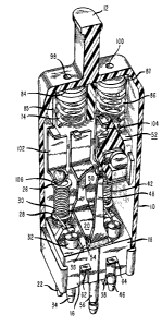
Referring collectively to FIGS. 1, 2, 3 and 4,
there is shown a solid state protector which is used for
protecting telecommunications' equipment against
spurious sneak currents and spurious surge voltages
which appear in a line interconnecting a customer's
equipment with a central office. The protector
comprises a housing unit 10, fabricated from a plastic
material, having a handle 12 which is used during
insertion in or removal from a protector block as
disclosed more fully in U. S. Patent No. 4,434,4~9
issued February 28, 1984 to Mr. Larry W. Dickey.
The protector comprises a base 14 fabricated
from a plastic insulator and having left half 16 and
right half 18. The two halves 16 and 18 are
substantially mirror images of one another. Halves 16
and 18 interpose, respectively, a mechanism for
protecting telecommunications equipment against spurious
sneak currents in the tip and the ring conductor path of
the line. Sandwiched between the two halves is a
grounding unit 20 for conveying the spurious currents
(or the spurious voltages) away from the
1301826
-- 6 ~
- telecommunications equipment to ground.
The left half 16 of base 14 comprises line
pin 22, on which one of the line conductors from the
customer's equipment is terminated. Referring to
FIG. 5, along with FIGS. 1 through 4, the upper part of
line pin 22 is shown surrounded by the inner surface of
spool or sleeve 24, aligned axially therewith, and
bonded thereto by a fusible material such as solder 25,
having a predetermined melting temperature. Sleeve 24
has an upper flange 26 and a lower flange 28. A coil of
insulated wire 30 is wound around the outer surface of
sleeve 24. One end of coil 30 is welded to the under
surface of sleeve 24 while the other end of coil 30 is
welded onto the upper end 32 of central office pin 34
are fabricated from copper alloy which is plated first
with paladium and then with gold. Sleeve 24 is made
from a good conducting material. Coil 30 is a wire
fabricated from an alloy such as nichrome which is
covered with nylon insulation. The normal flow of
current between a custom's equipment and central office
equipment will traverse line pin 22, solder 25, spool
26, coil 30 and central office pin 34. In response to a
spurious excessive current in the line, heat generated
in coil 30 will cause solder 25 to melt and release
spool 24 from its bond with line pin 22. Spool 24 will
then be forced downwards, as will be disclosed more
fully hereinbelow, to make contact with plate 36 of
grounding unit 20.
; Likewise, referring to FIGS. 1 through 4t the
current path in the other conductor in the customer's
line through the right half 18 of base 14 will traverse
line pin 38, sleeve 40, coil 42, central office pin 46
and then to the central office equipment. When a
spurious current develops in the line, the heat
generated as current flows through coil 42 will cause
the solder bonding sleeve 40 to line pin 38 to melt and
release sleeve 40 therefrom. Sleeve 40 will then make
~L301~326
contact with ground plate 36 in a ~anner to be described
more fully hereinbelow.
Grounding unit 20 comprises a spring having
front arm 48 and rear arm 50 formed from a single sheet
of temper hard copper. The two arms provide two
functions: 1) they secure surge voltage protection
device 52 in place and 2) they provide a path to ground
for the surge voltages. The two arms 48 and 50 are
joined by central plate 54 which is welded to ground
plate 36. Ground plate 36 is securely fastened to a
grounding pin 56. Grounding unit 20 is secured between
the left half 16 and right half 18 of base 14.
Referring more particularly to FIG. 4, there is shown a
recess 58 into which a projection 60 of grounding plate
36 fits in order to prevent the grounding plate from
accidental movement in either direction and touching any
conductive material on either left half 16 or right half
18 of base 14.
Left half 16 and right half 18 of base 14
have, respectively, tangs 62 and 64 which snap into
recesses 70 and 72 of housing 10 to secure the protector
components firmly therein. The rear of left half 16 and
right half 18, likewise, have tangs 66 and 68 to snap
into corresponding recesses (not shown) within housing
unit 10.
Voltage device 52, to be described more fully
hereinbelow, and for protecting against surges of
spurious voltages in the telephone line is secured
within arms 44 and 50 of grounding unit 20. A single
device is used for both protecting tip and ring
conductors. In the prior art, by contrast, separate
voltage protection was provided for tip and ring
conductors. See the aforesaid Dickey patent for an
example.
A metallic spring 74 fabricated from a good
conductive material such as solder plate phosphor bronze
is mounted over the left side 76 of voltage device 52.
130~82~
-- 8
Neck 78 of cap 80 is inserted into spring 74. The top
surface 82 of cap 80 is in contact with the upper, inner
surface 84 of housing 10. Spring 74 is lodged within a
guide 85 to prevent movement. Spring 86, likewise, is
placed over the right side 88 of voltage device 52.
Neck 90 of cap 92 is inserted within spring 86. Upper
surface 94 of cap 92 is in direct contact with the
upper, inner surface 95 of housing 10. In order to
prevent its movement, spring 86 is lodged within a guide
87. Caps 80 and 92 are fabricated from brass and have a
solder plate finish.
Openings 98 and 100 in the upper surface of
housing are offset from the center and provide an access
to the tops 82 and 94, respectively, of caps 80 and 92
to test for continuity of the line. The conductive path
for one side comprises cap 80, spring 74, metallic
clip 102 of voltage device 52, sleeve 24, solder 25 and
line pin 22. A similar path may be traced through the
other half. The inventive concept for test access is
disclosed in U. S. Patent Number 4,394,620 issued
July 19, 1983 to Messrs. A. R. Montalto et al.
In assembling the unit, caps 80 and 92 are
inserted, respectively, into springs 74 and 86 and
placed within guides 85 and 87 of housing 10 so that the
cap tops 82 and 94 are in immediate contact with the
inner surface 84 of housing 10 immediately under
openings 98 and 100. Voltage device 52 is then inserted
so that the tops of spring clips 102 and 104 make
contact, respectively, with springs 74 and 86. The
functions of these clips with be disclosed more fully
hereinbelow. Base 19 is next inserted within housing 10
so that upper flange 26 of sleeve 24 and the
corresponding flange of sleeve 40 make direct contact
with ridges 106 and 108 located, respectively, at the
bottom surfaces of spring clips 102 and 104. Base 14
when urged upwards causes voltage device 52 to compress
springs 74 and 86 until tangs 62 through 68 snap within
~01826
g
recesses such as 70 and 72 of housing 10.
Referring to FIGS. 6 and 7, there is shown the
shell of voltage device 52 of FIGS. 1 through 4. The
shell comprises a base 110 and a cover 112 fabricated
from an insulator. Base 110 has a central recess 114
for receiving a surge-suppressor 116 made from a single
chip which includes a silicon controlled rectifier and a
zener diode. The chip is sandwiched between two metal
discs, one being smaller than the other in diameter
Surge-suppressor 116 is polarity sensitive but functions
with six rectifier diodes 126, 128, 130, 132, 134 and
136, in a manner disclosed by the aforesaid patent
issued to R~ M. Bulley et al. Because of the steering
action of these diodes, the surge-suppressor current is
always in the same polarity. The surge-suppressor
generates heat on all polarities of the alternating
current cycle, that is, on both the positive and
negative parts of the cycle. Surgistor 116 is retained
in place by two metallic plates 118 and 120 which fit
within recesses 124 and 126, respectively.
Metallic plates 118 and 120 are fabricated
from electrical grade copper for good thermal
conduction. These plates 118 and 120 distribute the
heat generated from surge-suppressor 116 to a plurality
of diodes to be described hereinbelow. The ability to
distribute heat is important in the case of sustained
high voltage fault. The plates 118 and 120 are rounded
at the ends for ea~e in insertion in and removal from
base 110 in order to prevent damage thereto.
Recesses 115 and 117 through cover 112 receive
posts 111 and 113 which project from base 110. Cover
112 is bonded to base 110 by heat staking posts 111 and
113.
Six diodes 126 through 136 fit into recesses
138 through 148, respectively, in the opposite sides of
base 110. When the diodes are manufactured, two metal
discs having different diameters sandwich each diode
130~826
-- 10 --
therebetween. secauSe the aforesaid process is random,
some diodes will have the cathode adjacent to the larger
disc while others will have the anode adjacent to the
larger disc. In FIG. 7, the diodes are selected so that
all the anodes are adjacent to either one disc or the
other.
The diodes oriented so that their anodes point
in the same direction are held in place within the
aforesaid recesses in the sides of base 110 by spring
clips 106, 108 and 150 which are fabricated from
hardened phosphor bronze and then solder plated. Spring
clip 104 will secure diodes 126 and 136 within
recesses 138 and 148 of base 110. The top end 152 of
clip 104 is bent inwards so that it fits over and grips
the top surface of right side of base 110. It can be
seen that spring 86 rests directly on top end 152 of
spring clip 104. Furthermore, material adjacent to neck
154 which connects top end 152 to the rest of spring
clip 104 is removed to ensure that diode 136 is not
dislodged from recess 148 during assembly. Referring
briefly to FIGS. 12, 13 and 14, there are shown diagrams
which illustrate the insertion of the spring clips on
the base.
Spring clip 104 has a ridge 108 at the bottom
surface 109 thereof. The shape of ridge 108 provides a
constant surface area of contact with the upper flange
of sleeve 40 in all pivot po~itions of voltage
device 52. Likewise, the surface area of contact
between ridge 103 of spring clip 102 and upper flange 26
of sleeve 24 will be constant for all pivot of voltage
device 52. This is necessary to insure that the spring
clips 102 or 104 will not become entangled with the
upper flange of the respective sleeve or with the inner
sides of housing unit 10.
Furthermore, the shape of the ridge on spring
clips 103 and 104 is a pivot point that must continue to
transfer maximum heat to cause the corresponding sleeve
~3()1826
upon which each rests to snap down immediately in
response to a force from spring 74 to prevent arcing
between the ridges on spring clips 102 and 104 and the
upper flanges on sleeves 24 and 40. In the preferred
embodiment, the force exerted by each spring 74 or 86 is
about one pound.
Referring to FIG. 8, there is shown a circuit
diagram for the solid state protector 160 connected
between tip conductor 161 and ring conductor 163 of the
telephone line and tip conductor 165 and ring
conductor 167 of the central office. The solid state
protector comprises a voltage device 52 which in turn
comprises an surge-suppressor 116 and diodes 126 through
136. The operation of such a circuit is disclosed
substantially in U. S. Patent Number 4,408,248 issued
october 4, 1983 to Messrs. Raymond M. Bulley et al and
will not be repeated herein.
Referring to FIG. 9, the circuit of FIG. 8 has
been rearranged to show how the solid state components
are actually installed in the shell of FIGS. 7, 10 and
there is shown a recess 170 for receiving the
inwardly bent end 172 of ground spring clip 174. End
172 of ground spring clip 174 is below the top of
surface 176 of base 110 so that end 172 does not
accidentally touch springs 74 and 86 of FIG. 1. Ground
spring clip 174 secures diodes 128 and 134 within the
recesses in the sides of base 110. Arms 48 and 50 of
grounding unit 20 grips arms 178 and 180 of ground
spring clip 174, respectively securing voltage device 52
in position.
Referring more particularly to FIG. 10, there
is shown the rear view of voltage device 52 with spring
clip 102 removed to expose diode 132. End 152 of spring
clip 104 is shown on the top surface 176 of base 110.
End 172 of grounding spring clip 174 is shown within
recess 170, well below the surface 176 of base 110.
`i301826
- 12 -
Referring to FIG. 11, there is show~ the front
view of voltage device 52 with spring clip 104 removed
to exposed diode 126.
In FIGS. 10 and 11, the arms of spring
clips 102, 104 and 174 have convex shaped inner
surfaces 101, 105, 107, 109, 175, and 177 formed by
stamping. These convex surfaces grip the diodes and
retain them within their recesses in base 110.
Referring to FIG. 15, there is shown the solid
state protector of FIG. 4 after the device has operated
to release sleeve 40 and ground it. Assume a spurious
positive voltage appears in the line. This voltage will
travel from line pin 22 to flange 26 to ridge 106 to
spring clip 102 to diode 126 to plate 118 and then to
surge-suppressor 116. When the spurious voltage exceeds
260 volts, (or another predetermined level) surge-
suppressor 116 will begin conducting and the current
from the spurious voltage will flow through surge-
suppressor 116 through plate 120, through diode 134,
through the ground spring clip 174, to grounding unit
20, and safely leaves through ground pin 56. In the
event of a sustained fault, heat generated from
diodes 126 and 139 and surge-suppressor 116 will be
transmitted to flange 26 with line pin 22. The current
through the solid state components will generate heat
dnd cause the fusible material to melt, releasing sleeve
24. Force from spring 74 will cause voltage device 52
to push sleeve 24 immediately and forcefully downwards
to make contact with grounding plate 36 of grounding
unit 20. Negative spurious voltage will produce similar
actions.