Note: Descriptions are shown in the official language in which they were submitted.
~3~3~
HIGH FREQUENCY RESONANT POWER CONVERTER
FIELD OF THE lNVENTION
This invention relates to high frequency power converters with
resonant power throughput.
Back~round of the Invention
S A common disadvantage of many types of existing power converters
with single mode resonant power throughput is the disproportionate voltage and
current stress placed on the power train components relative to the level of power
throughput. Further disadvantages of existing resonant power converters include
limitation to a single switching device (i.e. single ended converters) and
10 limitations on the duty cycle range of the power switch. These single ended
converters have a unidirectional flux excursion in the power transformer and hence
need the added complexity of a core reset circuit. One such single ended resonant
zero current switching power converter having a unidirectional flux excursion inthe power transformer is disclosed in U.S. patent 4,415,959. It therefore requires
15 a comrnutation switch in order to reset the transformer core and to provide
continuous power to the load. It also has the aforementioned disadvantage of
limited duty cycle operation in order to prevent internal power circulation and to
assure power throughput. This limited duty cycle further causes the peak voltagestress on the power switch, rectifying diodes and resonanting capacitor to be
20 excessively large compared to the power being processed.
Power converters such as disclosed by F. C. Lee et al in APEC 86,
pages 84-89 in an article entitled "Secondary-side Resonance for High Frequency
Power Conversion" are double ended and have a bidirectional resonant path
perrnitting bidirectional flux excursions and hence eliminate a need for a core reset
25 circuit. A particular example described therein employs a resonating capacitor
which is shunted directly across the secondary winding. Such an arrangement
however still operates with a single mode resonance and places high stress on the
power train components. In addition the power circuit disclosed has a tendency to
circulate energy in the resonant circuit thereby blocking energy flow to the output
30 if the duty cycle of the power switch is too large ti.e.~ greater than 50%) or if
operated at very light load.
3~
~3~J115 ~37
It is apparent that the above described prior art exemplary converters operate
in single mode resonance and place a high stress on power train components. Attainable
power levels for given component capacities is therefore limited. A tendency to circulate
energy within a converter tank circuit at certain duty cycles is a further limit on the versatility
S of these prior art converts.
Brief Description of the Invention
A high frequency DC to DC converter having at least two phase diEferentiated
pulsed voltage sources, utilizes two phase differentiated unidirectional power flow resonant
circuits to permit multiple quasi resonant operation of the converter and thereby gain the
benefit of lowered EMI, high efficiency, lowered component stress and increased power
throughput. A particular embodiment is realized through a double ended push pull power
converter in which a resonating capacitor is added subsequent to the rectifier diodes but prior
to the output filter circuit. Parasitic capacitance oE the diodes and leakage inductance of the
power transformer is used as part of two oppositely phased resonant circuits in which each
resonant circuit is responsive to a voltage pulse of an associated power switch of the push pull
converters. Power flow in each resonant circuit is unidirectional and the single resonant
capacitor shared by the two resonant circuits is chosen relative to the impedance of a
subsequent filter circuit so that only the DC component of its voltage is transmitted to the
load.
The power converter circuit embodying the invention may as shown (but is not
limited to) operate in a frequency modulation mode, in which a cyclic interval is varied with a
fLxed pulse width predetermined for either on or off conditions of the power switch, with a
zero current switching condition achieved. Duty cycles above 50% are permitted without
impairing energy throughput. Other specific implementations of power converters which may
embody these principles include half bridge and full bridge inverters.
In accordance with one aspect of the invention there is provided a power
converter comprising: input means for accepting a DC voltage source, a power transformer
including a primary winding and a secondary winding; a resonating capacitor having first and
second access terminals; a first switch for applying the DC voltage source to the primary
winding in a first direction; a second switch for applying the DC voltage source to the primary
winding in a second direction opposite the first direction; a first secondary resonant circuit
connected to a first terminal of the secondary winding and including, a first inductance derived
in part from a leakage inductance of the transformer, a first rectifying diode and a connection
to the first access terminal of the resonating capacitor; a second secondary resonant circuit
~3t:~837
2a
connected to a second terminal of the secondary winding and including a second inductance
derived in part from a leakage inductance of the transformer, a second rectifying diode and a
coDnection to said first access of the resonating capacitor; the resonating capacitor having
resonant operation with both the first and second resonant circuits; and output means
5 connected to the resonating capacitor, having constant current sink characteristics and adapted
for accepting a load to be energized.
Brief Description of the Drawings
FIG. 1 is a circuit schematic of a regulated quasi resonant double ended DC to
DC converter operating in a fixed pulse, variable interval mode of operation and embodying
10 the principles of the invention;
FIG. 2 is a circuit schematic power train of a quasi resonant half bridge DC to
DC converter embodying the principles of the invention;
~o~
- 3 -
FIG. 3 is a circuit schematic of a power train of a quasi resonant full
bridge DC to DC converter embodying the principles of the invention;
FIG. 4 discloses current and voltage waveforms useful in explaining
the operation of the converter circuit disclosed in F~G. 1;
S FM. S is an equivalent circuit useful in describing the operation of the
circuit disclosed in FIG. 1.
Detailed Description
A push pull or double ended DC to DC converter adopted to operate
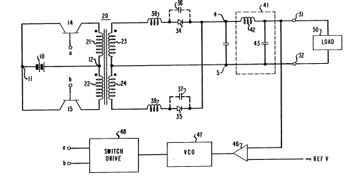
in a quasi resonant mode is shown in FIG. 1. A DC voltage source 10 connected
to the input terminals 11 and 12 is alternately applied to the primary windings 21
and 22 of power transformer 20 through the alternate ON-OFF switching of power
transistors 14 and 15, respectively. The secondary windings 23 and 24 are
coupled through rectifying diodes 34 and 35 to the opposite terminals 4 and 5 of a
resonating capacitor 40 respectively which is in turn connected across the output
15 filter and load transformation network 41 which is shown as comprising
inductor 42 and capacitor 43. A load 50 to be energized is connected to output
terminals 31 and 32 so as to shunt filter capacitor 43.
A control circuit for voltage regulation is shown which operates the
switching of the two power switching transistors 14 and 15 in a variable frequency
20 mode of operation. A replica of the output voltage sensed at output terminal 31 is
coupled to a comparator 46 which is also connected to receive a reference voltage.
The output error signal of the comparator 46 is applied to a duty cycle control 47
which may comprise a voltage controlled oscillator whose frequency is responsiveto the magnitude of the error signal. The duty cycle control output is applied to a
25 switch drive circuit 48 which may comprise a monostable multivibrator in which
one output is fixed in duration while the other output varies in duration in order to
accomplish regulation of the output voltage. The multivibrator output is appliedthrough a toggle gate which alternates the drive to the a and b terminals and hence
to the base inputs a and b of the two switching transistors 14 and 15. While
30 bipolar transistors are shown it is to be understood that power MOSFETs may be
used with drive applied to the gate terminals.
The power transformer 20 is preferably designed to have the leakage
reactances 38 and 39, which appear most prominently on the secondary
windings 23 and 24, and which are designed to be an integral part of the resonant
35 circuitry of converter. Discrete inductances, if needed, may be used in place of or
~3V~l~337
to supplement this leakage inductance. Each of the rectifying diodes 34 and 35
include the parasitic capacitances 36 and 37 which also are an integral part of the
resonant converter operation. These two capacitive elements may also be
supplemented or replaced by discrete capacitors if needed.
S Each rectifying diode 34 and 35 is connected to an opposite terminal4 and 5 of a resonating capacitor 40 whose capacitance is selected so that each
series connection of a leakage inductance, parasitic capacitance and resonating
capacitor resonates in response to a voltage pulse drive supplied by an associated
one of the switching transistors 14 and 15. The other oppositely phased resonant10 circuit not being driven at that time operates in a filter mode to reduce harmonics
applied to the resonating capacitor 40 and to the output. The output filter 41 is
designed to have an input impedance substantially exceeding the impedance of theresonant circuit driving it and hence transmits only the DC voltage of the
resonating capacitor to the output load 50. While filter 41 is shown as a single15 stage filter, multi stage filters with similar characteristics may also be used.
This circuit and its many advantages may be readily understood by
describing a typical cycle of steady state operation. The converter circuit basically
operates in a two phase mode of resonant operation in which a separate quasi
resonant signal processing event is independently associated with each switching20 transistor 14 and 15. A current flow in either one of the switching transistors 14
and 15 causes a current to flow in its associated quasi resonant circuit. The
current flow in the resonant circuit, resonates by charging the resonating
capacitor 40 first in one direction and then by continued resonant action
discharges the resonating capacitor 40 in the opposite direction. During the
25 resonant interval output load current is supplied through the rectifying diodes 34
and 35. When the conducting switching transistor turns off the resonating
capacitor finally discharges into the load. Circuit continuity during the
simultaneous nonconduction of the switching transistors 14 and 15 is provided bythe simultaneous forward conduction action of the rectifying diode 35 and 34
30 respectively. This sequence of operation is followed in each individual half phase
of operation of the push pull circuit, with each oppositely phased quasi resonant
circuit operating alternately and independently with respect to one another.
The principles of the circuit are readily ascertained by referring to the
various voltage and current waveforrns of F~G. 4 occurring during steady state
35 operation of the converter. Prior to the initial time To shown in FIG. 4 both
~3~i837
- 5 -
switching transistors 14 and 15 are biased nonconducting and a continuity
maintenance current drawn by filter inductor 42 is flowing through both rectifying
diodes 34 and 35. Each diode 34 and 35 ca~ries a current magnitude equal to halfthe output load current.
For the purpose of exploring circuit operation, assume that at time tO
as shown in FIG. 4, ~he transistor 14 has just been biased into a conducting state
and that transistor 15 has been nonconducting for a short interval starting prior to
to and for the time being remains nonconducting. A current shown by current
waveform 410 in FIG. 4, part A begins to flow in the circuit loop comprising thevoltage source 10, transformer winding 21 and the switching transistor 14. At this
moment there is no current flow in the circuit loop including transistor 15 and
hence a voltage equal in magnitude to twice the voltage of voltage source 10
appears across the transistor 15 as shown by voltage level 441 of voltage
waveform 440 in FIG. 4, Part D.
The current flowing through transistor 14 has a sinusoidal wave form
and continues conducting in duration sufficiently to complete a full half cycle
current waveforrn for which eventually terminates at t3. This is shown in current
waveform in FIG. 4, part A which extends from to to t3. A current shown by
waveform 470 in FIG. 4, part 6 is flowing through the rectifying diode 35 and at20 the time to has a value equal to 1/2 the output load circuit. It steadily increases in
value as shown by waveform 470 in FIG. 4, Part G to a value equaling the load
current at time tl and eventually to a peak value at time T2. All the current
exceeding the load current is directed into the resonanting capacitor 40 as shown
by waveform 460 in FIG. 4, Part F. Rectifying diode 34 also conducts a current
25 equaling 1/2 the load circuit at time to as shown by wavefonn 480 in FIG. 4,
Part H. This current is decaying and reaches zero value at time t1. Since the
output filter inductor 42 acts as a constant current sink only a current equal to the
steady state load current is transmitted into the load 50 and any excess current is
directed into the resonating capacitor 40. This charging current is shown by
30 waveform 460 in FIG. 4, Part F, and is shown extending between times tl and t4.
It completes a 3/4 period sine wave function at time t3 which is followed by a
fixed charging current which abruptly terminates at t4.
At time t1 the current in the switching transistor 14 and in the
associated conducting rectifying diode 35 is at a value substantially equal to the
35 full load current, as shown in waveforrn 470 in FIG. 4, Part G rarnp 490. The
~3~11337
current in diode 34, as shown by waveform 480 in FIG. 4, Part H has decayed to
zero by time tl leaving diode 34 fully reverse biased and nonconducting. After
time tl continues to increase in both transistor 14 and diode 35 a charging current
as shown by waveform 460 in FIG. 4, Part F begins to flow into the resonating
5 capacitor 40 causing its voltage to rise along curve 451 as shown by
waveform 450 in FIG. 4, Part E.
During the time interval from tl to t3 the current in conducting
transistor 14 rises to its peak value at time t2 as shown by point 411 and the
capacitor 40 is also charged to its peak value at this same time t2 as shown by
10 point 452 in waveform 450. This transistor current subsequently declines to zero
at time t3, and immediately subsequent to this time t3, the charging current
flowing through capacitor 40 goes negative and declines to a negative value
equaling the load current magnitude at dme t4 as shown by waveforrn 460 in
FIG. 4, Part F.
At time t3 the transistor 14 is biased nonconducting and current flow
in its related circuit loop shown by waveform 410 ceases. Similarly, current flow
in the rectifying diode 35 shown by waveform 470 has also dropped to zero. The
charging current in the resonating capacitor 40 stabilizes at the negative value of
the load circuit as shown by level 461 in waveform 460 shown in FIG. 4, Part F.
20 At the time t4 the rectifying diodes 34 and 35 are both individually conducting a
current equaling half the load current thereby providing a flyback current path to
provide the continuous load current to the filter inductor 42. The current flow in
the resonating capacitor 40 drops abruptly to zero at the end of the half cycle as
shown by waveform 460 and the voltage drop across each transistor 14 and 15 is
25 equal to the input voltage as shown by voltage levels 432 and 442 in FIG. 4,
Parts C and D respectively.
At the end of the half cycle neither switching transistor 14 or 15 is at
the moment to conducting. The voltage drop across each transistor is equal to the
input voltage as shown by voltage level 432 and 442 in FIG. 4, Parts C and D
30 respectively. At tl the switching transistor 15 begins to conduct current in
agreement with the waveform 420 in FIG. 4, Part B and the second half cycle is
initiated which proceeds in a manner similar to that described for the first half
cycle.
~3V1~37
- 7 -
It is apparent from the foregoing description that the quasi resonant
signal action is advantageously confined to the secondary part of the converter
circui~ and that since each half cycle is sufficient in duration to permit the desired
resonant action, the variable pulse width conduction interval on the primary side
S may be operated over a considerable range without adversely affecting the
resonant properties of the circuit. A particular feature of this arrangement is the
parasitic capacitance of the rectifying diode that shunts the rectifying diode and
the leakage inductance associated with the idle resonant circuit which in any half
cycle functions as a harrnonic filter and limits the application of harmonics to the
10 resonanting capacitor 40.
A half bridge embodiment of a power train embodying the principles
of the invention is shown in a schematic form in FlG. 2 in which two alternatelyconducting transistor switches 214 and 215 are shown connected in series
connection with this series connection being connected in shunt with the DC
15 voltage source 210 and the input voltage terminals 211 and 212. The switched
output voltage is taken from the junction node 216 of the two switching
transistors 214 and 215 and is applied to the primary winding 221 of
transformer 220. A resonant secondary circuit identical to the FIG. 1 is
alternately energized by secondary windings 223 and 224. The operation of half
20 bridge inverters is well known to those skilled in the art, and hence its operation
need not be discussed in detail.
A full bridge embodiment of the inverter is shown in FIG. 3 which
includes four switching transistors 314, 315, 317 and 318 in which two opposing
switches are operated in phase with one another to apply altemately directed
25 energy pulses to the primary winding 321 of transformer 320. The secondary
portion of the circuit is substantially identical in circuitry and operation to that
shown for FIG~ 1.
An equivalent circuit showing the electrical funcdonal operation of the
circuit schematic of FIG. 1 is shown in FIG. 5. The power transforrner is not
30 shown and hence a unity transforrnadon ratio is assumed. The two oppositely
phased resonant circuits are shown as having oppositely phased voltage pulse
source circuits 514 and 515 coupled to them. The first resonant circuit coupled to
voltage pulse source 514 includes a switch 535 which is operated as a diode
switch, a capacitance 537 shunting the switch and an inductance 539. The second
35 resonant circuit coupled to voltage pulse source 515 includes the diode
13V1~337
switch 534, a capacitance 536 shunting the switch and an inductance 538.
The two pulse voltage sources are operated during oppositely phased
intervals as that the two oppositely phased resonant circuits are pulsed or pumped
alternately during oppositely phased intervals. Each resonant circuit shares a
5 common resonant capacitor 540 which is connected at the input to the output
filter 541 which includes inductor 542 and capacitor 543. As each resonant circuit
is pulsed, the inductor of that circuit resonates within resonant capacitor 540 for
substantially a half cycle of operation with subsequent resonance being cut off by
the opening of the associated/switch diode. The inductor and capacitor of the
10 nonresonating circuit in the opposite phase operates as a harmonic filter to reduce
harmonics being applied to the resonating capacitor 540. Operation of the circuit
at FIG. S may be further specified in terms of the following equations specifying
the response and conditions of operation of the resonant circuits.
VCR (t) = VCR (tl ) [ C ¦ ( 1)
1 5 ICR (t) = ICR (t--1 )-- [ [VLR (t--I )--VOUT (t)]CR ~ (2)
ILR(t) = ILR(t--l) + ~[Vmax VCR(t--l)]~t]
V (t) = V (t 1) [~ILR(t)--lLR(t--l)]Ll ~ (4)
VMAX 1 VMaX tOFFmaX
I_ >Iload>Icritical>
~ zroN(Lc) LmatCh;ng
~3V~
where
CR is the capacitance of the resonating capacitor 540.
VMAX is the maximum voltage applied by the source (514) to the resonant
network.
S LmatChjng is the inductance of output filter 41.
VCR jS the voltage across the resonating capacitor CR 540-
ICR is the current through the resonating capacitor CR 540-
LR is the leakage reactance 539 or 538 forrning part of each resonantcircuit.
VLR is ~he voltage across the leakage reactance LR. 538 or 539.
ILR is the current through the leakage reactance LR~ 538 or 539.
r~
zroN(Lc) ;S defined as equal to 2