Note: Descriptions are shown in the official language in which they were submitted.
FA 40009/AJT~WJE
~3Vl~
A MULTIFUNCTION SWITCH INC~RPORATING
NCAP LIQUID CR~STAL
The present invention relates generally to liquid
crystal, and more particularly to a multifunction switch
incorporating nematic curvilinearly aligned phases
("NCAP") liquid crystal.
Liquid crystals are used in a wide variety of devices,
including visual display devices. The property of
liquid crystals that enables them to be used, for
example, in visual displays, is the ability of liquid
crystals to transmit light on one hand, and to scatter
light and/or to absorb it (especially when combined with
an appropriate dye), on the other, depending on whether
the liquid crystals are in a relatively free, that is
de-energized or field-off state, or in a strictly
aligned, that is energized or field-on state. An
electric field selectively applied across the liquid
crystals can be used to switch between the field-off and
field-on states.
There are three categories of liquid crystal materials,
namely, cholesteric, nematic and smectic. The present
invention relates in the preferred embodiment described
hereinafter to the use of liquid crystal material which
is operationally nematic. By "operationally nematic" is
meant that, in the absence of external fields, struc-
tural distortion of the liquid crystal is dominated by
the orientation of the liquid crystal at its boundaries
rather than by bulk effects, such as very strong twists
. ~
4`~k
3L 3~
-2- 1051-1882
(as in cholesteric material) or layering (as in smectic material).
Thus, for e~ample, a liquid crystal materia] including chiral
ingredients which induce a tendency to twist but which cannot
overcome the effects of the boundary alignment of the liquid
crystal material would be considered to be operationally nematic.
A more detailed explanation of operationally nematic liquid crys-
tal material is provided in U.S. Patent 4,616,903 which issued on
October 14, 1986 and is assigned to Manchester RhD Partnership.
Reference may also be made to U.S. Patent No. 4,435,047, issued
March 6, 1984, in the name of Fergason, entitled ENCAPSULATED
LrQUID CRYSTAL AND METHOD, assi-g~ed to Manchester R&D Partnership.
It is to be understood, however, that the various prin-
ciples of the present invention may be employed with any of the
various types of liquid crystal materials or combinations thereof,
including combinations with dyes. Reference to NCAP liquid crystal
apparatus or NCAP liquid crystal in connection with the present
invention is in no way intended to limit the present invention to
use with nematic liquid crystal materials. It is only for conven-
ience sake and in an effort to use an abbreviated term that des-
cribes the switch apparatus of the present invention that referenceis made to NCAP liquid crystal. Particularly, the term NCAP is
used because the preferred liquid crystal material is nematic or
operationally nematic liquid crystal and because in the field-off
condition, or any other condition which results in the liquid crys-
tal being in a distorted or randomly aligned state, the liquid
crystal structure is distorted to a curved form (hence curvilinear-
ly aligned) wherein the spatial average orientation of the liquid
crystal material over a capsule-like volume, for
13~
--3--
instance, is strongly curved and there is no substantial
parallel directional orientation of the liquid crystal
in the absence of a prescribed input, for example, an
electric field.
NCAP liquid crystals and a method of making the same and
devices using NCAP liquid crystals are described in
detail in the above-identified U.S. Patent No.
4,435,047. Briefly, NCAP liquid crystal comprises a
liquid crystal material dispersed in an encapsulating
medium. A NCAP liquid crystal apparatus is an apparatus
formed of NCAP liquid crystal material that is capable
of providing a function of the type typically inuring to
a liquid crystal material. For example, such a NCAP
liquid crystal apparatus may be a visual display device
that responds to the application and removal of an
electric field to effect a selected attenuation of
visible light.
Such NCAP liquid crystal apparatus may commonly include
a NCAP liquid crystal material positioned between two
electrodes wherein the electrodes are located on
respective substrates. Such apparatus may be used in
electronic devices that include a keyboard or push
buttons or an array of push buttons, or other types of
electrical switches and contacts used to control and/or
input information into an electronic device. Such an
electronic device may include any number of function
keys such as OFF and ON, START and STOP, TEST and
NO-TEST, etc. It will be appreciated that as the
: complexity of an electronic device increases, the number
of functions which the device can accomplish, and hence
the number of function keys or push buttons, also
increases. Due to space limitations and for other
considerations, it would be advantageous to limit the
number of function keys and associated displays for a
particular electronic device. One way of doing this is
to integrate a function key into an apparatus which
13~
-4-
displays the function.
The NCAP liquid crystal is particularly suitable for use
as part of a switch or function key for inputtinq and
displaying information. A membrane-type switch having a
flexible faceplate may be integrated with an NCAP liquid
crystal display apparatus wherein the information is
displayed by the NCAP apparatus with such display being
visible through the flexible faceplate of the switch.
Depression of the faceplate by application of a pressure
thereto, as might be applied by an operator, inputs
information and causes a change in the display. The
quality of the display of the present invention is not
adversely affected by application of a pressure to the
faceplate. In fact, the high quality of the display of
the present invention is unchanged by the application of
such a pressure.
With prior art liquid crystal display devices, it was
not possible to build a truly effective display
apparatus that includes a membrane-type switch for
inputting or receiving information. The reason for this
is that depression of a flexible faceplate of such a
switch, beneath which may be located a liquid crystal
material, would cause a flow of the liquid crystal
material away from the location at which pressure is
applied, adversely affecting the quality of the display.
Particularly, such a flow of liquid crystal produces a
change in the electrical and optical properties of the
liquid crystal, for example, a change in polarization
and the occurrence of birefringence, which adversely
affects the appearance of the display. For instance,
the application of a pressure to a prior art liquid
crystal display device utilizing a twisted nematic-type
liquid crystal material would cause such material to
lose its 90 twist, producing a detrimental optical
effect and thereby degrading the quality of the
--5--
display. Additionally, when such pressure i5 removed,
the liquid crystal material flows back to its original
position, producing another detrimental optical effect.
Unlike prior art liquid crystal displays, the NCAP
liquid crystal which forms a part of the switch
apparatus of the present invention is insensitive to
pressure; thus, there is no detrimental effect to the
display of such an apparatus upon the application of
pressure thereto. Particularly, by providing for
confinement of discrete quantities of liquid crystal
material, for example, in capsules, permits each
individual capsule or capsule-like volume to in effect
operate as an independent liquid crystal device with the
result that the display effected by the switch apparatus
of the present invention is not pressure sensitive.
That is to say, the encapsulated liquid crystal material
will not flow away from the point at which pressure is
applied thereto to any significant extent to adversely
affect the quality of the display.
In view of the foregoing, an object of the present
invention is to provide a multifunction key or switch
incorporating NCAP liquid crystal wherein an effective
display is provided.
Another object of the present invention is to provide a
multifunction key or switch including a NCAP liquid
crystal which is insensitive to pressure wherein the
switch is adapted to input and display information such
that the information displayed may be dependent upon the
function or operation controlled.
As may be seen hereinafter, the switch apparatus o~ the
present invention includes a switch means for inputting
information and for displaying the same. The switch
means incorporates NCAP liquid crystal material. NCAP
liquid crystal material comprises a liquid crystal
13~3~8~;
74260-24
material and containment means for inducing a generally non
parallel alignment of said liquid crystal material which in
response to such ali~nment at least one of scatters and absorbs
light and which in response ~o a prescribed input reduces the
amount of such scattering or absorption.
The prescribed input is preferably of the
electromagnetic type and, more particularly, an electric field. A
pair of electrodes may be provided to apply the electric field.
The electrodes are located on opposite sides of the combination o~
the liquid crystal material and the containment means. The
electrodes may be adapted to ef fect a visual output display of
information.
The switch means may comprise a flexible substrate
having a conductive segment formed thereon. The flexible
substrate may be positloned in a spaced substantially parallel
relationship to one of the electrodes of the NCAP apparatus. The
flexible substrate has sufficient flexibillty to deflect toward
the electrode in re~ponse to the application of a pressure
thereto. At least a portion of the flexible substrate is
deflectable toward the electrode means so that the conductive
segment thereon is coupled to the electrode means to effect the
~isual output display.
The lnvention may be summarized, according to one broad
aspect, as a switch apparatus comprising a switch means having a
flexible portion for inputting informatlon and for causing a
display, said switch means incorporating a llquid crystal
apparatu including the combination of a liquid crystal material
and containment means for inducing a distorted alignment of said
liquid crystal material which in response to such alignment at
least one of scatters and absorbs light and which in response to a
prescribed input reduces the amount of such scattering or
absorption, the combination of the liquid crystal material and
containment means being supported by a ~lexible substrate in
spaced substantially parallel relation to said flexible portion,
wherein a change in the display is effected by application of said
prescribed input by deflection cf said flexible portion with at
~L3~1~81~
7~260-24
least a par~ of said flexible substrate also being deflected, the
combination of the liquid crystal material and containment meanæ
substantially resistant ~o flow away from the area of deflection
of said part of said flexible substrate such that the capability
of said liquid crystal apparatus to induce said distorted
alignment and to reduce the amount of such scattering or
absorption remains substantially unaffected by the deflection.
The switch apparatus of the present invention will be
described in more detail hereinafter in conjunction with the
drawings wherein.
Figures 1-3 are schematic views illustrating a multi-
function ~witch in accordance with the present invention;
Figure 4 iB a schematic view of an alternate embodiment
of the present invention utilizing a dot matrix
'~d
13~
--7--
configuration to display inf~rmation;
Figure 5 is a schematic view of ano~her embodiment of
the present invention;
Figure 6A schematically illustrates an integrated
control panel in accordance with the present invention;
Figure 6B is a view along line 6B-6B of Figure 6A;
Figure 7 schematically illustrates an array of switches
in accordance with the present invention utilized to
form a keyboard;
o Figure 8 is an end view of one of the switches of Figure
7;
Figure 9 schematically illustrates yet another embodi-
ment of the present invention;
Figure 10A schematically illustrates an integrated
multifunction keyboard in accordance with the present
invention; and
Figure 10B is a view along line 10B-lOB of Figure 10A.
Referring now to the drawings, in which like components
are designated by like reference numerals throughout the
various figures, attention is first directed to Figures
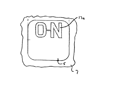
1 and 2. Figures 1 and 2 show a key or push button 5
, that is adapted to control the on/off function of an
electronic device 7. Of course, it should be apparent
that the present invention may be used to control and
display almost any function of a device, such as
START/STOP, HIGH/LOW, FORWARD/REVERSE, etc. Addition-
ally, it should be apparent th~t the present invention
may be utilized with many different type~ of devices,
for example, calculating equipment, communication
~3~ 6
--8--
equipment, household appliances such as microwave ovens,
computer-aided design equipment, and computer aided
manufacturing equipment.
Figure 1 depicts the device in the on mode wherein the
word "ON" is displayed. Figure 2 shows the device in
the off mode with the word ~OFF" displayed. Key or push
button 5 is a membrane-type switch. It includes a
flexible front substrate 9 that is adapted to deflect
toward a second substrate 18 when pressure is applied
thereto, as schematically illustrated by arrow "An.
Preferably, substrate 9 is a polyester film having
sufficient flexibility to deflect under a pressure as
might be applied by an operator of a typical keyboard.
Substrate 9 has an electrode or conductor 6 formed
thereon that is adapted to contact an electrode 8
located on substrate 18. Particularly, when an operator
applies pressure by depressing substrate 9 tas shown by
arrow "An), the gap between substrates 9 and 18 will
close, and electrode 6 will electrically contact elec-
trode 8, operating the function that switch 5 controls.Alternatively, switch 5 may operate on the basis of a
change in capacitance between conductors 6 and 8 as
would occur when substrate 9 is depressed. In such an
embodiment, there would be no need to have conductors 6
and 8 contact one another.
The present invention further includes a NCAP liquid
crystal apparatus, indicated generally by reference
numeral 10. The apparatus includes a NCAP liquid
crystal material 11 which may be supported on a
substrate 12 having an electrode 13 located thereon.
~he apparatus further comprises a second electrode 14
mounted on the side of substrate 18 remote from
electrode 8. Membrane switch 5 and NCAP apparatus 10
thus in effect share a common substrate or electrode.
As illustrated, conductive segment 6 is positioned in a
13~B~f~
g
spaced substantially parallel position relative to
electrode 14. The NCAP liquid crystal material 11 may
include a liquid crystal material 20 more or less
contained within the confines or the interisr volume of
a capsule 22 or encapsulating medium. The NCAP liquid
crystal material comprises a plurality of uch capsules
or an encapsulating medium in which liquid crystal
material is dispersed.
A quantity of liquid crystal material is csnfined or
contained in volumes within the encapsulating medium,
for example, in a solid medium as individual capsules or
dried stable emulsions. Such volumes may be discrete
volumes, that is, once formed, they ordinarily remain as
individually distinct entities or separate entities.
Such separate entities or discrete volumes, however, may
also be interconnected, for example, by one or more
passages. The liquid crystal material would preferably
be in both the discrete vol~mes and in such in*er-
connecting passages. Thus, the internal volumes of
respective capsules may be fluidly coupled via one or
more interconnecting passages. All of the aspects and
features of the present invention vis-a-vis individual
unconnected capsules have been found to be applicable to
an arrangement of capsules that have one or more inter-
connecting passages.
In the embodiment illustrated, electrode 13 comprisestwo electrically isolated patterns of conductors 13a and
13b (see Figures 1 and 2), each of which may be selec-
tively energized. Conductor 13a may be configured to
display the word "ON" when it is energized, and conduc-
tor 13b the word ~OFF" when it is in an energized state.
Electrode 14 preferably has a rectangular shape that
approximates the outline of the pattern of electrode 13.
Of course, it should be understood that electrode 13 may
comprise some other pattern of conductors, for example,
13V~
--10--
conductor 13 may comprise a plurality of 5 x 7 dot
matrix characters wherein individual conductive segments
of the matrix may be selectively energized, as is known
in the art, to display either the words ~ON~ or "OFF".
For that matter, such a dot matrix arrangement may be
driven to display any other alpha or numeric display
desired, including a display of more than two functions
or a display of other information. For example, as
shown in Figure 4, a membrane-type push button 95 may be
depressed to provide a temperature reading at a certain
location (nLoc. B") wherein the temperature is a
variable parameter. In the embodiment of Figure 4, a
plurality of dot matrix characters are used to provide
the displayed information, which includes the tempera-
ture and its location within the process. In thisrespect, it is also possible to drive the dot matrix
arrangement of Figure 4 such that the temperature at
another location may be displayed by push button 95.
Other possible configurations and operations o~ push
button 95 and its associated dot matrix characters are
possible in the context of the present invention.
The embodiment shown in Figures 1-3 does however offer
the advantage of reducing the complexity of the cir-
cuitry required to control and drive the display, sincesuch circuitry need only selectively apply a voltage
across one or the other of the two conductors 13a and
13b in response to the operation of switch 5.
A voltage may be selectively applied to electrodes 13
and 14, and hence across liquid crystal material 11, by
means of a switching circuit 16 (see Fi~ure 3). Cir-
cuits that accomplish the ~unctions of switching circuit
16 are well known to those skilled in the art, and thus
switching circuit 16 is not described in any detail. As
shown, appropriate electrical leads connect the switch-
ing circuit to electrode 14, conductive segments 13a and
13b, and electrodes 6 and 8 of switch 5. Switch 5
~3~
controls the on and off functions of device 7 through
switching circuit 16. Device 7 is switched between its
on and off modes by depressing substrate 9 of switch 5.
Switching circuit 16 also controls the application of a
voltage across electrode 14 and either conductive
segment 13a or 13b, depending upon the mode (on or off)
of device 7.
By way of example, if device 7 is in the off mode,
conductor 13b will be energized, that is, a voltage will
be applied across electrode 14 and segment 13b, and
hence across the NCAP liquid crystal material located
therebetween, such that the molecules of the NCAP liquid
crystal are in the desired alignment to permit the
transmission of light to display the word "OFF".
Conversely, no voltage is applied across segment 13a,
and thus it is in a de-energized or field-off state
wherein the liquid crystal material scatters and/or
absorbs light to obscure the word rON". Pressing key or
push button 5 to turn device 7 on causes electrode 13a
to be energized and electrode 13b to be de-energized
such that the word "ON" is displayed and the word "OFF"
is obscured.
Substrates 9, 12 and 18, and electrodes 6, 8, 13, and 14
may be optically transmissive so that liquid crystal
apparatus 10 is capable of controlling the transmission
of light therethrough in response to an electric field
applied across electrodes 13 and 14. Alternatively,
electrode 13 and/or substrate 12 may be optically
reflective or may have thereon an optically reflective
coating so that reflection by such reflective coating of
incident light will be a function of whether there is an
electric ~ield applied across the liquid crystal ll.
A plurality of NCAP liquid crystals arranged in one or
more layers are preferably applied to substrate 12 in a
manner such that the NCAP liquid crystals adhere to
13~911~i~6
~12- 1051-1882
electrode 13 and substrate 12. The material of which capsules 22
are formed is suitable for binding or otherwise adhering the cap-
sules to the substrate and the electrode. In one embodiment,
capsules 22 are formed of a polyvinyl alcohol (PVA). In the pre-
ferred embodiment, the liquid crystal material is dispersed or
entrapped in a latex medium. In either embodiment, substrate 12
may be a flexible polyester film, such as Myla ~, that has been
precoated with a 90 to 5000 ohms per square, and preferably 450+ 15
ohms per square, layer of indium tin oxide (ITO). The electrode
coated surface of substrate 12 is etched, as is well known in the
art, to form conductive segments 13a and 13b. Of course, materials
other than ITO may be used to form electrode 13. A Mylar~film
with a precoated ITO electrode, known as Intrex, may be used in
the present invention. Intrex may be purchased from Sierracin
of Sylmar, California.
As noted, latex entrapped NCAP liquid crystal is used in
the preferred embodiment. Latex entrapped NCAP liquid crystal
comprises the entrapment of liquid crystal in a latex medium. The
latex is a suspension of particles. The particles may be natural
rubber or synthetic polymers or copolymers. A latex medium is
formed by drying a suspension of such particles.
Briefly, latex entrapped NCAP liquid crystal may be for-
med by mixing a suspension of latex particles and liquid crystal
material wherein the liquid crystal material has been previously
emulsified in an aqueous phase. Alternatively, all components
may be combined
~4 ~rc, ~ a ~ ~
13~3~8~6
-13-
prior to emulsifying the liquid crystal material. The
mixture may then be applied to substrate 12 and elec-
trode 13. As the mixture dries, it adheres to the
electrode coated side of the polyester film. When
dried, the latex particles form a latex medium with
particles of liquid crystal dispersed in therein.
A specific method for making latex entrapped NCAP liquid
crystal may comprise first emulsifying 36 grams of the
liquid crystal ROTN701 (manufactured by Hoffman La Roche
of New York, New York) in a solution containing 14 grams
of a 124 aqueous solution of PVA and 1 gram of ~he
surfactant TWEEN 20 (available through ICI Americas
Incorporated of Wilmington, Delware). The liquid
~rystal is added continuously while the solution is
mixed with an impeller blade at 3500 RPM. When the
particle size of the liquid crystal is about 1-5
microns, 49 grams of Neorez R-967 (manufactured by Poly-
vinyl Chemical Industries, Wilmington, Massachusets),
containing 40~ latex particles by weight, is added with
slow mixing of less than 1000 RPM until the mixture is
homogenous. This material may then be cast with a
doctor blade or other suitable means onto substrate 12
and electrode 13.
After the NCAP liquid crystal material has dried on
electrode 13 and substrate 12, substrate 18 and elec-
trode 14 formed thereon may be laminated onto the
surface of the latex entrapped NCAP liquid crystal.
Substrate 18 may also be a flexible Mylar~ film
precoated with a 90 to 5000 ohms per square, preferably
a 450 + 150 ohms per square, layer of ITO to form
electrode 14. Electrode 14 and substrate 18 are
substantially optically transparent to electromagnetic
radiation in at least a portion of the visible range.
Electrode 14 and Mylaro film 18 may be formed from the
Intrex material.
t r r~,J e, r~
13~8~
-14-
Electrode 8 on the side of substrate 18 remote from
electrode 14 may be formed by depositing an optically
transmissive conductor material, such as ITO, on the
surface of substrate 18. As noted, substrate 9 may be a
polyester film having sufficient flexibility to deflect
toward substrate 18 when push button 5 is depressed so
that electrode 6 on substrate 9 conductively contacts
conductor 8. Conductor 6 is preferably formed from an
optically transmissive conductor material such as IT0,
and substrate 9 is also transparent.
Figure 5 illustrates an alternate embodiment of the
present invention. In this embodiment, NCAP liquid
crystal apparatus 10 and a membrane-type switch 50 share
a back or common substrate 120. As discussed hereto-
fore, NCAP apparatus includes a NCAP liquid crystalmaterial 11 supported on substrate 120 havin~ an elec-
trode 13 located thereon. The NCAP apparatus also
includes a second electrode 14 mounted on a substrate
180.
Electrode 13 may be configured to form a pattern of
electrically isolated conductive segments (including a
dot matrix or other similar pattern) for effecting any
desired display, such as a numerical display. Electrode
14 may have a rectangular shape that approximates the
outline of electrode 13.
As discussed hereinabove, substrates 120 and 180, or
portions thereof forming a display or viewing area, and
electrodes 13 and 14 may be optically transmissive so
that the NCAP liquid crystal apparatus is capable of
controlling the transmission of light therethrough in
response to an electrical field applied across elec-
trodes 13 and 14. Alternatively, electrode 14 and
substrate 180, or a portion thereof through which the
display is to be viewed, may be transparent, and
electrode 13 andlor mounting substrate 120, or a portion
:~3~8~6
-15-
thereof in a display area, may he optically reflective
or have an optically reflective coating thereon.
Preferably, substrates 120 and 180 are formed from a
flexible polyester ~ilm. These substrates and the
electrodes formed thereon may be fashioned from the
Intrex material referred to above.
In the embodiment of Figure 5, membrane-type switch 50
is spaced from and horizontally disposed with respect to
NCAP apparatus 10. Switch 50 includes a flexible front
substrate 90 that is adapted to deflect toward substrate
120 when pressure is applied thereto, as by a human
operator and as schematically illustrated by arrow "A".
Substrate 90 is preferably a polyester film having such
sufficient flexibility. As illustrated, substrate 90 is
substantially parallel to and spaced from substrate 120.
Front substrate 90 has an electrical conductor 60
located thereon that is adapted to contact an electrical
conductor 62 located on rear substrate 120. Particular-
ly, when an operator presses key or push button 50,
20 substrate 90 is deflected towards substrate 120 such
that the gap therebetween closes with conductor 60
contacting conductor 62 to actuate the function that
switch 50 controls.
Appropriate circuitry for operatively coupling switch 50
to NCAP apparatus 10 and for driving the display may be
included on substrate 120. Such circuitry may include
LSI metal oxide semicnnductor ~MOS) chips 64 mounted in
a single dual-in-line package suitable for direct
assembly to substrate 120. Appropriate circuit paths
would be provided for interconnecting the display
electrodes of NCAP apparatus 10 and the conductors of
switch 50 to the chips 64. Such conductive paths may be
,~,4
formed on and/or through substrate 120, as is well known
in the art, and a conductive flexible tape 66, such as
~Scotchlink Connector Tape manufactured by the Elctro/IEP
Division of the 3M Company, Inc. of St. Paul, Minnesota,
c~ L~
~ 3Vl~
-16-
may be utilized to connect conductors 60 in circuit with
chips 64. All the timing, logic, memory, resistors,
switch functions, and drivers for the display and switch
may be contained in chips 64.
A spacer 200 may be provided between NCAP apparatus 10
and switch 50 to separate substrates 90 and 180.
Alternatively, the spacer may be eliminated, and
substrates 90 and 180 would comprise a single flexible
substrate.
The embodiment of Figure 5 may also be modified by
locating a dielectric material between substrate 90 and
substrate 120. The dielectric material would form an
insulative barrier between conductors 60 and 80.
Application of pressure to flexible front substrate 90
(as shown by arrow "A"), however, would cause the
dielectric material to be displaced from between
conductors 60 and 80 so that electrical contact could be
made therebetween. The embodiment of Figures 1-3 could
be similarly modified by locating a dielectric material
between conductors 6 and 7.
The embodiment of Figure 5 provides for the integration
of the display, the switch, and the circuitry for
driving and controlling the display and switch functions
in a single unit. Such a unit may be utilized as an
integrated control panel for various devices such as
household appliances. For instance, as shown in Figures
6A and 6B, an integrated control panel 100 may be
. utilized as a control panel for a microwave oven.
Such a control panel 100 can comprise two displays 102
and 104, and any desired number of keys or switches, for
example switches 106a-1061, for inputting information to
control the operation of a microwave oven, for instance.
The displays may be the numerical display shown that is
effected by a pair of NCAP apparatus 10 located between
~3~
substrates 108 and 110 ~see Figure 6B). The control
panel may further include a frontface 112 which includes
appropriate openings for the displays and switches. The
switches would preferably be membrane-type switches
wherein at least a portion of substrate 108 correspond-
ing to a particular switch area would be sufficiently
flexible to effect an input of information. For
instance, switch 106b may comprise conductors 160 and
180 formed on respective substrates 108 and 110 wherein
10 the area of substrate 108 corresponding to switch 106b
is sufficiently flexible such that with the application
of a pressure thereto (representated by arrow "A")
conductor 160 contacts conductor 180 to effect a
selected input of information. Alternatively, as
discussed heretofore, the switch may function by a
change in the effective capacitance between conductors
160 and 180.
A printed overlay 130 (see Figure 6B) may be located
over the respective switch areas 106a-1061 to identify
the function controlled and/or the information to be
inputted. As shown, by way of example, switch 106a is
overlaid with the numeral "on. As discussed heretofore,
the necessary control circuitry for driving the displays
and for effecting an input of information by means of
the switches would be provided by chips 164 on substrate
110. A flexible conductive tape 66 may be used to
interconnect the conductors and display electrodes on
substrate 108 in circuit with the circuitry on substrate
110. Appropriate circuit paths would be formed on
and/or through the respective substrates.
Electrical leads 166 may be used to interconnect the
control panel circuitry to the circuitry of the
microwave oven, for instance, with which the control
panel is to be utilized. In this manner, an integrated
control panel may be constructed and subsequently
assembled into the microwave oven by simply connecting
13~
-18-
leads 166 to the appropriate circuitry in the oven.
Such an integrated control panel would be particularly
useful in assembling high volume, low costs products.
An array of switches constructed in accordance with the
present invention may be used to construct a keyboard as
illustrated in Figure 7. The keyboard 70 may comprise a
plurality of switches or keys 5' arranged adjacent to
one another in columns and rows. Each switch 5' may be
adapted to display an associated function that it
controls. A computer, such as a microprocessor 90 on a
printed circuit board (PCB) 92 (see Figure 8), may be
utilized in conjunction with the switches to control
their associated functions. The computer may also be
used to implement control over the selective application
of the electrical field across the liquid crystal
material of each switch.
Switches 5' of keyboard 70 may be direct-addressed. The
conductive paths which connect the electrodes of the
respective switches to a suitable circuit means, for
example one located on PCB 92, for driving the displays
and for effecting an input of information by means of a
switch may be formed on flexible arms or extensions, as
shown in Figure 8. Particularly, substrate 12' on which
electrode 13' is formed may include flexible extensions
12a' and 12b' on which are formed an appropriate number
of conductive paths for connecting electrode 13' to a
circuit means. For example, if electrode 13' was formed
to comprise a plurality of dot matrix characters wherein
. individual conductive segments of the matrix can be
selectively ener~ized and are direct driven to effect
the desired display, the numerous conductive paths
required for interconnecting the conductive segments to
the circuit means would be formed on flexible arms 12a'
and 12b'. Similarlyr substrate 18' may include a
flexible extension 18a' having suitable conductive paths
formed thereon for connec~ing electrodes 8' and 14' to
13a~1~386
--19--
the circuit means. Substrate 9' may also include a
flexible arm 9a' having a conductive path formed thereon
for connecting electrode 6' to a suitable circuit means.
~he respective flexi~le extensions may be sharply bent
as shown to permit interconnection of the electrodes on
the substrates to the circuit means.
Substrates 12' and 18' and their associated extensions
12a' and 18a' may be formed from the Intrex material.
The conductive paths on the extensions may thus be
formed by etching the ITO coated surfaces thereof. The
conductive path on extension 9a' of substrate 9' may be
formed by depositing a conductor material, such as ITO,
on the surface thereof.
The use of the flexible extensions as described above
permits the respective switch apparatus 5' of keyboard
70 to be located in close proximity to one another such
that the distance between switches is minimized.
Additionally, the flexible extensions provide a maximum
viewing or display area 80 for each switch, as the
electrodes 13' and 14' which effect the visual output
display may extend to the outer perimeter 80a of viewing
area 80.
Another embodiment of the present invention is shown in
Figure 9. In this embodiment, the flexible extensions
or arms heretofore described are replaced by a flexible
conductive tape 82. The conductive tape electrically
connects the electrodes on the various substrates to a
circuit means for driving the display and for inputting
information via the switches. The conductive tape may
be an electrically-conductive, flexible tape such as
Scotchlink Connector Tape manufactured by the
Electro/~EP Division of the 3M Company, Inc. of St.
Paul, Minnesota. This type of connect~r tape may
comprise a plurality of conductor stripes 82a formed on
a film backing 82b. Of course, where the tape is
13~
-20-
utilized to interconnect a single electrode to a circuit
means, the conductive tape need only include one con-
ductor stripe. The connector tape further includes an
adhesive material for electrically connecting the
conductor stripes to the respective electrodes as well
as to a suitable circuit means. Such connections may be
accomplished by means of heat bonding.
An integrated multifunction keyboard may be constructed
in accordance with the present invention. Such a
keyboard (see Figures 10A and 10B~ may include a
plurality of integrated multifunction function switches
200. This keyboard is particularly suitable for use as
a menu for computer-accessed information. For instance,
the keyboard may be used to access the entertainment
activities available in a given area. By way of
example, depressing the key 200 displaying the term
"MOVIES" would cause a display on the keyboard of all of
the movies in the particular area. The display of such
movies would be provided by the display electrode
pattern of switches 200. Further depressing a switch
200 displaying a certain movie may cause a display of
additional information, visible through the faceplates
of some or all of switches 200, relating to the movie
selected, such as the location or locations and times at
which the particular movie is playing.
Such pyramiding of information may be accomplished by
means of a suitable microprocessor and software for
operating the same. The display of information would be
effected by the display electrode pattern of the various
multifunction switches, the display being visible
through the faceplates of the switches. The surface of
the display would be extremely flat and preferably
multiplexing techni~ues would be utilized to drive the
various displays.
13~
-21-
Figure lOB illustrate a suggested construction for a
switch 200 of the keyboard. The construction of switch
200 is similar to that illustrated in Figures 1-3.
Switch 200 may comprise a flexible faceplate or
substrate 209 that is adapted to deflect toward a
substrate 218 when pressure is applied to substrate 209,
as schematically illustrated by arrow "An. Faceplate
209 includes a conductor 206 that is designed to contact
conductor 208 on substrate 218 when an operator
depresses faceplate 209, thereby effecting an input of
information by means of the switch. Alternatively,
switch 200 may operate on the basis of a change in
capacitance betwe~n sonductors 206 and 208, eliminating
the necessity of having conductor 206 contact conductor
15 208.
Key 200 would further include an NCAP liquid crystal
apparatus 210 for displaying information, which may be
observed through faceplate 209. As heretofore
described, the NCAP apparatus would include an NCAP
20 liquid crystal material 11 located on a substrate 212
having an electrode 213 formed thereon. A further
electrode 214 may be located on substrate 218 on the
side thereof remote from conductor 208.
Electrode 213 preferably comprises a dot matrix pattern
of conductive segments wherein individual conductive
segments may be selectively energized to display the
requested information. Electrode 214 may comprise a
similar pattern of conductive segments or a single
common electrode, as illustrated.
Chips 264, as discussed previously, may be located on
the backside of substrate 212. The chips provide the
necessary timing, logic, memory, and switch functions
for driving the display in response to the input of
information by means of the switches. Appropriate
circuit patterns may be formed on and/or through
13~
-22-
substrates 209, 212 and 218, and flexible conductive
tape 266 may be utilized to connect the respective
conductors 206 and 208, and display electrodes 213 and
214 in circuit with chips 264.
In the context of the present invention, it would be
possible to construct a keyboard of the type shown in
Figure lOA by utilizing a single faceplate for the
plurality of switches, and one pair of substrates for
all of the NCAP display apparatus. Such displays would
simply be formed between selected portions of the
substrates, and similarly, selected portions of the
faceplate would have sufficient flexibility to permit
proper operation of the switches.
Although certain specific embodiments of the invention
have been described herein in detail, the invention is
not to be limited only to such embodiments, but rather
~nly by the appended claims.