Note: Descriptions are shown in the official language in which they were submitted.
~30~94
APPARATUS AND METHOD FOR PHASE
MODULATING OPTIC:AL SIGNALS
IN A FIBER OPTIC ROTATION SENSOR
BACKGROUND OF THE INVENTION
5This invention relates generally to rotation sansors and particularly to fiber
optic rotation sensors. Still more particularly, this invention rslates to apparatus
and methods ~or modulating light signals in a fiber optic rotation sensor to
maximize operational efficiency and minimize errors.
A fiber optic ring interferometer typically comprises a loop of fiber optic
10material having counter-propagating light waves therein. According to the Sagnac
effect, the wave traveling in the direction of rotation of the loop has a lon~er transit
time throu~h the loop than the wave travelin~ opposite to the direction of rotation.
This differsnce in transit time is seen as a shift in the relative phases of the waves.
The amount of phase shift depends on the rotation ra~e. Aftsr traversin~ the loop,
15the counter-propagating waves are combined so that they interfere to form an
optical output signal. The intensity of the optical output signal varies as a function
of the type and amount of interference, which is dependent upon the relative
phase of the counter-propagating waves. The optical output si~nal produced by
the interfersnce of the countsr-propagating waves varies in intensity as a function
2 Oof the rotation rate of the loop. Rotation sensin~ is accomplished by detectin~ the
optical output signal and processing it to determine the Fotation rate as a function
of the phase shift.
A fundamental propert~ of fiber optic ring rotation sensors is reciprocity.
Ordinarily, any disturbance of the optical path affects both waves in the same way,
25even if the two waves are not subjected to the disturbance at exactly the sametime or in th0 same direction. Th0re are however, some disturbances which vary in
time with a period comparable to the propagation time oS the waves throu~h ~he
sensing loop. Thar~ are also nonreciprocal disturbances which do not have the
sams effect on the waves. The nonreciprocal disturbances are the ~araday Effect
3 Oand th~ Sagnac Effoct. These are two typss of disturbances which do not obey the
reciprocity principle.
If no nonreciprocal disturban~es appear in tho counterpropa~ating waves,
the phase differance between th~ two waves when th0y are r~combined in the
separating and mixing coupler is zero. The det3ction ~nd proc~ssing apparatus
130~894
--2--
respond to signals indicative of the optical power of the composite wave obtained
after the counterpropagating waves have been mixed together. This power may
be broken down into a constant component and a component proportional to the
cosine of the phase shift. The component proportional to the cosine of the phase5 shift appears in the signal only when there are nonreciprocal disturbances in the
optical path of the waves.
In tha measurement of low amplitude disturbances, which correspond to
low rotation rates, the component containing the cosine Qf the phase shift. term is
very small since the phase shift, ~, is nearly zero. It is then n6cessary to add a
10 fixed additional phase shift or nonreciprocal bias to the waves to increase the
sensitivity of the measurement of the phase shift. One situation of interest is where
the new phase shift measured is ~ + rc/2. In this cass, the sensitivity is
maximized since the term to be measured is proportional to cosine (~ 12),
which is proportional to sine ~. For small Q~, ths sine term has ma~imum slope,
1 5 so that small changes in ~ ar~ measurable.
Thsre have however been difficulties in implementing a device that
introduces a sufficiently stable nonreciprocal bias to be usable in a navigationgrade rotation sensor.
Arditty 6t a/. in Canadian Patent No. 1,154,955 disclosed a process for
20 shifting the operating point of a ring interferometer without r~quiring either a
nonreciprocal bias or a great stability of the phenomena used to shift the operating
point. That patent discloses a process for modulating the phass of waves in a ring
interfcrometer that comprises thc steps of forming a ring wave guide in which two
electroma~netic waves travel in opposite directions, providing a source of
25 electromagnetic energy, separating and mixing the electromagnetic waves in the
rin~ and detecting the interference of the waves in the ring to deterrnine the phase
difference bstween them. Arditty et al. further disclose periodic and symmetric
modulation of the phase of the waves with a period function ~ (t) = ~ (t + 2~)
where ~ is the time for each of the waves to travel over the path defined by the ring.
3 0 Arditty further disclosss det~ctin~ the phase differencs at the frequency 2~ and
discloses a phase modulation device fQr implementing the process.
. . .
894
SUMMARY OF THE INVENTION
The apparatus according to the invention is a closed ioop feedback system
for processing signals output from a fiber optic rotation sensor ~hat ~uides a pair of
counterprspagating light waves in a sensing loop of optical fiber and combines
5 the waves to produce an interference pattern indicative of the phase difference
between the waves. The present invention provides apparatus and method for
shi~in~ the operating point of a fiber optic rotation sensor to obtain an increased
sensitivity in the measurement of the sagnac phase shift betwean the
counterpropagating beams.
This invention provicies modulation of phase of waves in a fiber optio
~yroscope comprising means forming a ssnsing loop that guides two
counterpropagating optical waves, a source of electromagnetic energy, means for
separating and mixing the electromagnetic waves for detecting interference of the
waves to indicate the phase difference between them. The pressnt invention
15 provides periodic modulation of the phase of the waves in accordance with a
periodic function having a frequency equal to fs ~whsre ~ is the transit time
for an optical wave in the sensing loop. The interference pattern of the two waves
is periodically samplsd at a frequency equal to the modulation frequency. The
fundamental principle of this invention is that modulating the phase of the waves
2 0 in the fiber optic rotation sensor at a frequency f = n+l) where n is an integer and
is the transit time of the light wave in the sensing loop provides significant
operational advantages. Modulating the light at these frequencies provides most
efficient operation of the phase modulator by requiring the lowest voHage, current,
power and electric or magn0tic field. These frequencies also provide suppression25 of Raylei~h backscanering induced noise by modulating this noise outside the
detection bandwidth. These frequencies also provide elimination of parasitic
polarization modulation caused by the phase mDdulator and csr~ain nonlinearitiesin the phass modulation.
The apparatus comprises means for modulating the phase of light waves in
30 the sensing loop with a periodic function having a frequency equal to~
where n is an inte~er and ~ is the ~tansit time of a li~ht wave in the sensing loop;
and dstector moans for datectin~ si~nals output from ths sensin~ loop at a
13~)1894
frequency producing a detector signal indicative of the phase difference of tha
waves. The apparatus may further includes means responsiv~ to the detector
signal for controlling the modulating means to null the detector signal, the control
signal being indicative of ~he rotation rate of the sensing loop.
The apparatus according to the invention may further include gating m0ans
connected to the means for producing an electrical signal indicative of the phase
difference of the waves; rate demodulating means connected to the output of the
gating means for determining the rate and direction of rotation; and additional
demodulating means connected to the output of the gating means to adjust the
calibration of rate demodulating means.
The method of the invention for processing signals output from a fiber optic
rotation sensor that ~uides a pair of counterpropagating light waves in a sensing
loop of optical fiber and combines the waves to produce an interference pattern
indicative of the phase difference between the waves, comprises the steps of
modulating the phase of light waves in the sensing loop with a periodic functionhaving a frequency equal lo (2n~ 1); and detecting signals output from tha
sensing loop at a frequency producing a detector signal indicative of the phase
difference of the wavss. The method of the invention may further include ths step
of controlling the modulating means to null the detector signal, the control signal
2 O being indicative of the rotation rate of the sensing loop.
The method according to the invention may further include the steps of
gating the electrical signal indicative of the phase difference of the waves;
demodulating the gated electrical signal to determine the rotation rate and
direction; and demodulating the gated electrical signal to adjust the calibration of
2 5 the rotation rate signal.
BRIEF DESCRIPTION OF THE DRAWINGS
Figure 1 illustrates a fiber optic rotation sensor and circuitry for processing
the optical signal output from the Sagnac ring to null the Sagnac phase shift;
Figure 2 is a perspectivs v~ew of an inte~rated optics phase rnodulator that
3 O by may be included in the fber optic gyroscope of Figure 1;
Fi~ur~ 3 is plan view of the pha$~s modulator of Fi~ure 2;
Figure 4 is an end elevation vlew of the phase modulator of Fi~ures 4 and
5; and
~.~0~894
Figure 5 illustrates another apparatus for practicin~ the present invention.
DESCRIPTION OF THE PREFERRED EMBODIMENT
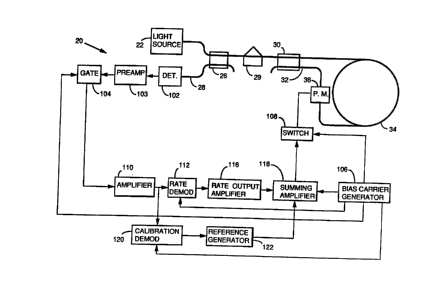
Refsrring ~o Figure 1, a fiber optic rotation sansor 20 includes a light source
22 that supplies coherent light to an optical fiber 24. The optical fiber 24 guides
5 the source bearn to a fiber optic directional coupler 26, which couples ligh~
between the optical fiber 24 and an optical fiber 28. Light that propagates through
the fiber optic directional coupler 26 and remains in the optical fiber 24 is guided
to a polarizer 29 and then to a second fiber optic directional coupler 30. The fiber
optic directional coupler 30 couples light between the optical fiber 24 and a third
1 0 length of an optical fiber 32.
Light that propagates through the fiber optic directional coupler 30 and
remains in the fib~r 24 then propa~atr~s to a sensin~ coil 34. Li~ht that enters the
sensing coil 34 from the optical fibar 30 forms a clockwise wave in tha coil. The
sensing coil 34 may be formed from a separate optical fiber, or it may be formed in
15 a portion of ths optical fiber 24. After passing throu~h the sensin~ coil 34, the
clockwise wave enters a phase modulator 36.
Light that the fiber optic directional coupler 30 couples from the optical fiber24 into the optical fiber 32 forms a counterclockwise wave. Ths optical fiber 32may be either a ssparate fiber or a portion of the optical fiber that forms the
20 sensing coil 34. Th0 counterclockwise wave first passes through the phase
modu!ator 36 before entering the sensing coil 34.
The clockwise wavs and the counterclockwise wav0 have the same phass
before they pass throu~h the sensing coil 34. If the sensing coil 34 is rotatingabout a line through the plane of the coil, then the waves expenence a phase shift
25 relative to each other. The clockwise wave enters the fiber optic directional coupler 30 after passing through the phase modulator 36, and the
counterclockwise wave entars the fiber optic directional coupler 30 after passing
through the sensing coil 34. Part of the counterclockwise wave propagates
throuyh the fiber optic directional coupler 30, and the rernainder of the
3 0 counterclockwise wave couplss into the end 38 of the optical fibsr 32. A portion of
the clockwise wav~ r~mains in the fiber 32, and the remainder of the clockwisa
wave is coupled into the fiber op~ic direc~ional coupler 26 by the fiber optic
diroctional coupler 30.
A fiber optic directional coupler suitable for use in sin~le mode applications
1301~94
as the couplers 26 and 30 of Figure 1 is described in the March 29, 1980 issue
of Electronics Letters, Vol. 28, No. 28. pp. 260-261 and in U.S. Patent 4,493,528
issued January 1~, 1985 to Shaw et al. That patent is assigned to the Board o~
Trustees of the Leland Stanford Junior University.
A suitable structure for the polarizer 2g is described in U.S. Patent No.
4,729,622 issued to the present inventor and assigned to Litton Systems, Inc.,
owner of the present invention. Other devices for polarizing a signal
propagating in an optical fiber may also be used in the present invention.
Re~erring to Figures 2-4, the phase moduiator 36 may comprise an
optical waveguid~ 40 formed on a substrate 42 of an electrooptically ac~ive
material such as lithium niobate. The structure shown in Figures 2-4 is only an
example of a suitable electrode arrangement for providing the desired phase
modulation. Other phase modulation devices and other electrode configurations
may be used to practice the invention; therefore, the scope of the invention is
not restricted to the particular structure shown. A pair of electrodes 44 and 46ara attached to the substrate on opposite sides of the waveguide 40. The
electrodes 44 and 46 may be formed on ths substrate 42 by vacuum deposition
of aluminum. The optical waveguide 40 may be formed in the substrate 42 by
first depositing a strip of titanium on the substrate 42 and heating it to diffuse the
titanium into the substrate 42. The resulting waveguide 40 has a generally
rectangular cross section as shown in Figures 2 and 4. The fiber 32 must be cut
to have two ends 33 and 35 that are butt coupled to opposite sldes of the optical
waveguide 40 as shown in figuros 1 and 11.
Application of a voltage across the electrodes changes the refractive
index of the optical waveguide 40 by means o~ the electrooptic effect. The transit
time of a light wave through the waveguide 40 is the product of the length of the
waveguide and its refractive index divided by the speed of light in vacuum.
Changing the refractive index of the optioal ~vaveguide 40 thus changes the
transit time of an optical signal through it. Because of the sinusoidal nature of
the electromagnetic fields that comprise the light wave, the change in transit
time is seen as a change in phase of the wave.
Other structures that provide phase modulation of an optical wave
propagating in a fiber may be used in the present invantion instead of tha phasemodulator described above. A phase modulator structure suitable for use in the
. . .
1;~01~4
invention includes a length of optical fiber wrapped around a mandrel formed of a
piezoelectric material (not shown). Application of voltage to the piezoelectric
material causes it to sxpand or contract, thereby changing the len~th of the fiber.
The length change causes a change in transit time of a light wave in the Siber. This
change in transit time is seen as a modulation of the phase of the waves.
The signal processing circuitry shown in Figure 1 shows one way to apply
ths principle of the invention. The illustrated circuilry is by way of example only
and is not intended to limit the scope of the invention to require the use of any
particular circuitry. The circuitry of Figure 1 may be formed of either analog or
1 0 digital components.
The circuitry of Figure 1 applies a phase shift signal to tha phase modulator
36 to shiSt the phase of the waves with a signal f, (2~ ~ where ~ is the ~ransit
time of the light waves in the sensing loop 34, and n is an integer.
The output of the dstector 102 is input to a preamplifier 103, which amplifies
15 the signal and conditions it for input to a ~ate 1û4. The detector 102 may be a
commercially availabl0 device such as Motorola MFOD 2404, which includes a
photodiode and a hybrid amplifier with wide bandwidth characteristics. The gate
J 104 may be a CMOS analog switch such as the Siliconix DG271. A bias carrier
generator 106 controls both the gate 104 and a switch 108, which is connected to20 the phase modulator 36. When the gate 104 is conductive, the output of the
preamplifier 102 is input to an amplifier 110. The amplified signal is output from
the amplifier 110 and then input to a rate demodulator 112 and to an amplitude
demodulator 120. The ratc amplifier produces a si~nal that is directly proportional
to the output rate of the sensor loop 34. This rate signal is is then summed with the
2 ~ bias carrier signal and switched on and off as shown in Figure 2. The resuiting
signal is then used to close the rate servo loop. The bias carrier ~enerator 106also provides an actuating signal to the rate demodulator 112.
The output of the amplifier 110 is also input to a calibration demodulator
120, which receives a signal trom the bias carrier generator 106. The signal output
30 trom the calibration demodulator 120 is input to a raference generator 122, which
provides an output to control the ~ain of the summing amplifier 118.
The phase modulator signa! pre,f~rably will cause a component of the total
phase shift ~qual and opposite to'ths rotation-~nduced phase shift. An opposite
13Q189
--8--
polarity bias signal is applied to the phase modulator 36 to null the rotation rate of
the sensing loop 34 as seen by the photodetector 102. The amplitude of the signal
applied to tha phase modulator 34 to null the rotation rate of the sensing loop 34 is
directly propor~ional to the output rate of the gyro.
Figure 5 shows a second circuit for practicing the invention. The basic
structure of the fib~r optic rotation sensor included in Figure 5 is identical to that of
Figure 1. Components in Figure ~ that are the same as the corresponding
components in Figure 1 have the same reference characters in both drawings.
These components are the source 22, couplers 26 and 30, fibers 24, 28 and 32,
phase modulalor 36, sensing coil 34, detector 102, preamplifier 103, gate 104,
ampiifier 110, calibration demodulator 120, rotation rate demodulator 112, rotation
rate amplifier 116 and referance generator 122. Items shown in Figure 5 that arenot in Figure 1 hava reference characters beginning with the numeral ~2".
The signal output from the amplifier 110 is input to the amplitude
demodulator 120 and to the rotation rate demodulator 112. Both the calibration
demodulator 120 and the rotation rate demodulator 112 may be commercially
available demodulator circuits such as the Siliconix DG271. The rotation rate
demodulator 112 recovers rate error signals from the s0nsing loop. These rotation
rate error signals are amplified by the rotation rate amplifier 116, which may be a
signal amplifying device such as a Burr Brown 3550 operational ampiifier. A~er
amplification, the rate error signals are conver~ed to digital signals by an analog to
digital converter 204 that is connected to the output of the the rotation rate
amplifier 116. The analog to digital converter 204 may be any suitable device,
such as a Burr Brown PCM 75 16 bit analog to digital converter for converting
2 5 analog electrical signals to digital.
The digital rotation rate error signals from the analog to digital converter
204 are input to a microprocessor 206, which may be a Logic Devices Inc.
429C01 bit slice microprocessor. Thc microprocessor 206 is used to accumulate
the error signal, scale it and sum it with the bias carrier signal.from a microcode
3 0 and state ~enerator PROM devico 208. The microprocessor 206 is operated as a
state dsvice. It ~enerates the appropriate bias carrier signal. The microprocessor
206 is operated conventionally and is clockad and controlled in its states by a set
of PROMs 208 ~enerate the ~ate and d~modulation signals. A clock 210 supplies
clock signals to the microprocessor 206 . The clock 210 also providss clock
1301~94
signals to a counter 212 ~hat supplies signals to the PROMs 208.
The digital output of the microprocessor 206 drives both the f0edback
digital to analog converler 202 and the digital rotation rate output interface, which
may be a 16 bit output register 214.
The calibration demodulator 120 provides an output signal to an amplitude
reference amplifier 200, which drives the reference generator 122. The output ofthe reference generator 122 is input to the digitai to analog converter 202. Thedigital to analog converter 202 provides signals to a video amplifier 216, whichdrives the phase modulator 36. The calibration demodulator 120 recovers a signalfrom the amplifier 110 and uses this signal to control the gain of the digital to
analog converter 202 to scale its full scale output to be 2~.
The digital to analog converter 202 may be be a Burr Brown 710, which is a
16 bit device. The gain of the digital to analog converter 202 is controlled by using
the reference amplifier 200 and the reference generator 122 to scale the output of
the digital to analog converter 202 and the video amplifier. The output video
amplifier 216 may be any suitable amplifier, such as a Comlinear CLC 210 high
speed operational amplifier or as was for amplifying electrical signals in the
frequency range commonly used for video signals.