Note: Descriptions are shown in the official language in which they were submitted.
23
MAGNETO-OPTIC MEMORY
Technical Field
The invention is a magnetic structure involving magnetic material
and coatin~s useful in a variety of applications including magneto-optic memory
5 storage devices.
Back~round of the Invention
Magnetic materials play an important role in mode~n technology.
They are used in permanent magnets and electromagnets often as part of a motor
or other mechanical device. Magnetic materials are also used in various memory
10 devices, transformers, inductances, etc. Various new magnetic materials have
advanced this technology considerably and are responsible for the development ofnew devices useful in modern technology.
Typically, these magnetic materials are made up of such elements as
iron, nickel, cobalt, rare-earth metals and alloys of these elements (e.g., FeTb,
15 FeCoTb, etc.).
Particularly attractive in modern technology is the development of
magnetic materials for various kinds of memory devices. The development of
computers and modern technology has resulted in the need for high density, high
capacity memory devices of various characteristics and properties. Various
20 magnetic-type devices such as magnetic computer disks have been used for high`
density memory unit~ because of low cost, ~asy fabrication, etc.
Optical disks are also used as memory storage units. Optical disks
incorporate low-power lasers to access or read the storage surface. Because laser
radiàtion can be directed onto a very small spot on the storage surface, magnetic
25 storage density is very high, as much as 500 megabytes for an ordinary size disk.
The major disadvantage of conventional optical disks is that they
cannot be erased and reprogrammed. Although conventional optical disks are
useful in a number of applications, disks with very high bit density that are
erasable and reprogrammable are extremely desirable.
A variety of disk structures has been proposed for an erasable,
reprogrammable disk. Particularly attractive are disks $hat work on the magneto-optic principal where magnetic states are used to store the information. In thistype of device, the info~nation is contained in magnetic states in the disk, usually
in the form of a region of uniform magnetization in a magnetic material with
35 Curie temperature well above room temperature. Reading the disk is done
optically generally with a laser using the polar Kerr effect. Changing the direction
of magnetization is achieved by heating locally the area of interest and using a
~L
~30~L92:~
magnet or electromagnet to produce the desired magnetization. Such devices have
been described in a number of references including a paper entitled "Magneto-
optic Recording Technology" by Mark H. Kryder, Journal of Applied Phvsics 57
(1), pages 3913-3918 (15 August 1985) and a paper by I. Sander et al. entitled
5 "Digital Magneto-optic Recorder", published in Optical Data Storage, Di Chen,
F,ditor, Proc. SPIE 382? page 240 (1983).
The nature of the magnetic medium determines, to a large extent, the
characteTistics of the optical disks, such as data storage density, writing speed, etc.
Amorphous thin films of rare-earth transition-metal alloys have shown great
10 promise as materials for magneto-optical mass storage, giving high storage
densi~ies and reasonable writing speeds. It is known that the magrletic and
magneto-optical properties of such alloys are very sensitive to composition
variations. Such composition variations may be caused by oxidation, corrosion orby chemical reaction or interaction (e.g., diffusion) with other materials interfacing
15 with the magnetic materials.
A variety of materials have been investigated as the magnetic storage
medium for magneto-optic disks. In addition to various transition-metal elementsand rare-earth elements are a variety of alloys comprising rare-earth elements.
Typical elements are iron, nickel ~nd cobalt from the transition-metal elements,20 terbium and gadolinium from the rare earth metals and other elements such as
bismuth and tin. Particularly attractive are alloys of TbFe and various
compositions of TbFeCo typically ranging from Tbo 30FeO 3~,Co0 38 to
Tbo 24,~eo,35C0.41'
In order to prevent corrosion of these magnetic films, they are often
25 covered by various non-magnetic films such as SiO, SiO2, Si3N4, etc. Althoughsuch non-magnetic protective films improved stability greatly, much greater
stability and inertness to external conditions are desirable. Various magnetic
materials and protective films for such magnetic materials are discussed in a
variety of references including an article by P. Bernstein and C. Gueugnon, Aging
30 Phenomena in TbFe Thin Films, Journal of Applied Physics 55(6), pages 1760-
1762 (March 15, 1984) and T. C. Anthony et al., The~nal Stability of Magneto-
opeic Quadrilayers, Journal of Applied Physics 59~1), pages 213-217 (January 1,
1986).
It is highly desirable to have a magnetic material structure which is
35 inexpensive, highly stable over long perîods of time and is suitable for various
magnetic devices including memories and optical disk memories.
~3~1~23
SummarY of the ~nvention
The im~ention is a device comprising magnetis material and a
multiple-layer protective coating, one layer being a barrier layer to protect
against interdiffusion and reaction with an outer protective film that alter theS composition of the magnetic material and another layer (chemically inert layer)
made of chemically stable material to protect against chemical alteration such as
oxidation and corrosion. The invention is particularly useful for magnetic or
magneto-optic memory storage media such as optical disks. Magnetic materials
are well known in the art including metals, alloys, compounds, amorphous
10 materials (e.g., splat cooled magnetic glasses or ribbons) etc. Generally, the
magnetic materials have Curie temperatures above room temperature, often up
to about 1000C. Many magnetic materials used in optical disks have Curie
temperatures between 50 and 600C, more often in the range of 50 to 250C.
For magnetic storage media, typical magnetic materials are alloys of iron and/or15 cobalt and rare earth metals, such as terbium and gadolinium, as well as other
materials such as bismuth and tin. The barrier layer usually covers at least part
of the surface oE the magnetic material. The barrier layer is typically made of a
material that prevents diffusion through it even in thin layers and that does not
react either with the magnetic material or the protective film. Typical barrier
20 layer materials are niobium, tantalum and zirconium with niobium preEerred.
The chemically inert layer is usually a material (typically metal) that forms a
passivating layer on its surface such as aluminum, chromium, nickel or titanium.Often, for a memory device such as an optical disk, magnetic material, diffusionbarrier and corrosion barrier are in the form of thin films with thicknesses
25 varying between 1n and several thousand Angstroms, and this structure is
mounted on a substrate with perhaps other thin films to provide reflectivity,
adhesion, spacing, etc. The entire structure is often covered with a protective
coating for ease in handling. These structures provide excellent protection
against alteration of the magnetic media over long periods of time and insure
30 stability of the magnetic properties of the magnetic material even when heated
by a laser.
- 3a -
~30~;23
In accordance with one aspect o~ the invention there is provided a
device comprising a magnetic structure, said magnetic structure comprising: a.
magnetic material with Curie temperature above room temperature; b. a first
region comprising barrier material contacting at least a portion of the magneticS material; c. a second region comprising chemically inert material contacting at
least a portion of the first region in which said chemically inert material
comprises at least one metallic substance selected from the group consisting of
metallic element and metallic alloy, said metallic substance being substantiallypassive to atmospheric conditions; d. said barrier material having the property of
10 preventing interdiffusion into or out of the magnetic material and not reacting
with the magnetic material or chemically inert material; and e. said chemically
inert material being chemically inert to the barrier material.
lSrie~ I)escription ~f the Drawin~
FIG. 1 shows a magnetic structure for a particle with magnetic
15 material surrounded by barrier layer surrounded by chemically inert layer;
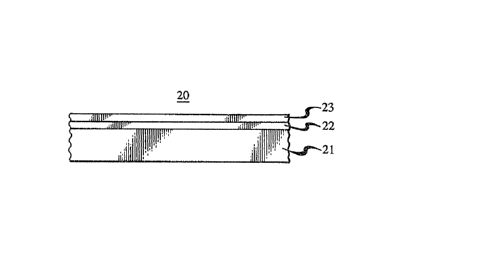
FIG. 2 shows a magnetic structure made up of more or less flat
layers of magnetic materials, barrier material and chemically inert material;
.~
130~9~3
FIG. 3 shows a magnetic structure useful for optical disks where the
layers are attached to a substrate;
FIG. 4 shows a magnetic structure useful for optical disks in which a
reflector and 1/4 wave plate are incorporated to enhance the detection system for
5 bit in~ormation; and
FIG. 5 shows another magnetic structure useful for optical disks that
yields enhanced optical intensity in the magnetic material layer by judicious use of
dielectric layers and reflector layer.
Detailed Descriptioll
The invention is based on the discovery that long term stability for
magnetic materials can be achieved by providing not only a chemically inert layer
to protect against chernical attack of the magnetic material but also a barrier layer
between magnetic material and chemically inert layer to prevent reaction betweenthe chemically inert layer and the magnetic material an~ to prevent diffusion of15 material into or out of the magnetic material. The invention is applicable to a
large variety of devices employing magnetic or magneto-optic materials. Typical
devices are motors, generators, magnetic circuit elements such as transformers,
chokes, etc.
Typically, the stmcture comprises magnetic material, barrier layer and
20 chemically inert layer.
The nature and composition of the barrier layer is particularly
important. It should prevent any reaction between the chemically inert layer andthe magnetic layer and it should prevent interdiffusion of material either into the
magnetic material or out of the magnetic material. In particular, it should prevent
25 diffusion of the material in the chemically inert layer from diffusing into the
magnetic rnaterial. Also, the material of the barrier layer should not itself
interdiffuse with the magnetic material.
Other desirable characteristics of the barrier layer material are as
follows. It should have little or no intersolubility with the magnetic material.30 This can usually be determined from phase diagrams. The barrier material should
not react with the chemically inert layer. This is more likely a problem where adielectric material is used as the chernically inert layer.
Although various types of rnaterials may be used as the barrier layer,
a metal or alloy is usually preferred. Such materials are more easily deposited on
35 a surface by such techniques as vacuum evaporation, sputtering, e-beam
deposition, etc. Extremely thin layers of metals and alloys are more likely to
provide defect-free, uni~orm coverage of the magnetic material with a minimum of
~L3~1L9;~3
holes and voids. Some preference is given to metals rather than alloys because of
ease of deposition and composition stability.
Although the invention is applicable to a large variety of magnetic
devices, most interest is centered on magnetic memories of various kinds,
S including magneto-optic memory storage units.
A variety of magnetic materials is useful in magneto-optic memory
storage units. Generally, the magnetic material for magneto-optic disks is an
alloy, often including a rare earth metal. Ihe magnetic material should be
amorphous to avoid grain-boundary noise.
Magnetic materials should also support submicrometer domains,
provide adequate magneto-optic effects for good signal-to-noise ratio for memory"reading", have Curie temperatures to insure stable magnetic domains around
room temperature but permit "writing" on laser heating and be stable over long
periods of time. An early magnetic materials used for magneto-optic recording
15 was MnBi because of its large Kerr rotation.
The most popular magneto-optic recording materials today are
amorphous rare-earth transition-metal alloys, which are deposited by vacuum
deposition, sputtering or e-beam deposition. In spite of the fact that no materials
have yet been found with a Kerr magneto-optic rotation comparable to that of
20 MnBi, better slgnal-to-noise ratios are achieved because the amorphous films have
a mirror-like sur~ace and produce much less noise than polycrystalline MnBi
films. In addition, the deposition procedure ~or the amorphous alloys is relatively
easily achieved in a production environment.
The magnetic properties of the rare-earth transition-metal alloys are
2S governed by antiferromagnetic coupling between the rare-earth and the transition-
metal atoms. The magnetic moment per unit volume of the rare-earth atoms is
usually different from that of the transition-metal atoms so that a Neel-type
~erromagnetic material results. Coercive force is usually reduced on increasing
temperature. To write domains into these materials with a focussed laser beam,
30 the temperature of the magnetic material is usually raised above room temperature.
The most popular materials ~oday are alloys containing one or more of
the rare-earths Gd, ~b, and Dy in addition to one or more of the transition metals
Fe and Co. GdFe and GdCo films typically exhibit very strong temperature
dependence of coercivity near the compensation temperat~re but a rather low
35 coercivity at temperatures aw~y from the compensation point. The smallest
domain diameter that can be supported by a magnetic thin film wi~h no field
applied is
13~1~23
do = ~IM Hc. (1)
where 6 is the domain wall energy, M is the magnetization and Hc is the coerciveforce. Unless special techniques are used in making GdCo and GdFe films,
submicrometer domains are not stable in them because the product M Hc is too
S small.
One of the earliest materials ~o have been used that could support
submicrometer domains was TbFe. TbFe and GdTbFe alloys remain one of the
most popular rnagneto-optic recording materials. The Kerr rotation angle for these
films is about 0.25. Ihey can be deposited by vacuum evaporation or sputtering.GdTbCo alloys have adequate intrinsic coercivity, M ~c, to support
submicrometer domains. The Co-based alloys typically provide slightly higher
KelT magneto-optic rotations (~ 0.3~) than the Fe-based alloys, especially at
higher temperatures because their Curie point is higher. In addition, GdCo filmstypically suffer corrosion less than GdFe films. Slightly higher Kerr rotations
15 ha~e been obtained with TbFeCo alloys. It should be emphasized that improved
magnetic materials, which provide more optimum properties, may be found in the
future. Thiclcness of the magnetic layer may vary considerably. Typical range ofthickness is 10 to 5000 Angstroms with 25 to 3000 pre-ferred. Optimum thickness
often depends on the particular material but generally the magnetic material
20 should be thick enough to insure a continuous film which is pore free. Magnetic
and optical properties often limit thickness.
The diffusion barrier may be made by a variety of materials. Metallic
elements are often most suitable because they can be deposited in extremely thinlayers that are often very effective in preventing diffusion.
Typical metals used for the diffusion balrier are niobium, tantalum,
zirc~nium, titanium, silicon, copper, tungsten and molybdenum. Preferred are
niobium, tantalum and titanium with niobium most preferred. Solid solutions of
these metals and alloys of these metals may also be useful (for example to obtain
an effective balTier with a thinner layer), but for the most part metallic elements
30 are preferred because of ease of deposition and ease in regulating composition and
layer structur~. Layer thickness f~r the barrier layer may vary sonsiderably often
depending on where in the magnetic disk structure the layer is located. For
example, if light from the laser reading the disk must pass through the balTier
layer, small layer thickness is at a premium and thicknesses between 10 and
35 500 angstrom are usually preferred. Less than 10 angstrom, the layer is not likely
to be continuous (pore-free and minimum defect density) and greater than
500 angstrom seems unnecessary7 wasteful of material and difficult to get light
~3~1~923
through where that is necessary. The range from 50 to 200 angstrom is usually
preferred.
The chemically inert layer should be chemically stable particularly to
exposure to air and atmospheric conditions up to a temperature of at least
5 200 degrees (preferably 300 degrees or higher). Elevated temperatures are used in
the "erase" and "writing" steps for optical memories. In addition, the chemically
inert layer should not react or alter the barrier layer either at room temperature or
at the elevated temperatures referred to above.
Various materials may be used in the chemically inert layer including
10 metals, alloys, and dielectrics (e.g., glasses, oxides, etc.). Typical dielec~ics are
SiO2, SiO, silicon nitride, borosilicate glasses, phosphosilicate glass, A12O3,
Cr2O3, TiO2, and nickel oxide.
Preferred for the chemically inert layer are metals and alloys with the
properties described above. Metals and alloys are pre~erred because of ease in
lS obtaining thin, pore-free and defect-free layers. Generally, metals or alloys that
form passivating layers in air that are stable up to 200 or 300 degrees C are
preferred. Typical metals are chromium, aluminum, nickel, titanium and silicon
with aluminum Md chromium most preferred. Typical alloys are the various
alloys of chromium and iron (e.g., the stainless steels) and the various nickel-
20 based alloys te g., Inconel, etc.). Layer thickness for the chemically inert layersmay vary over large limits. Where light is to pass through the layer (e.g., in the
read phase of an optical disk device), small thickness is at a premium. Typical
thicknesses are between 10 and 500 angstrom with 20 to 150 angstrom preferred.
The lower limit is set so as to insure pore-free, defect free layer and sufficient
25 thickness to support an oxide film on the layer. Greater thicknesses than theupper limit make it difficult for light transmission and often is not necessary.Where the chemically inert layer is serving another function, (reflector, dielectric
layer, etc.), greater thicknesses (e.g., several thousand Angstroms) are often used.
The invention may be useful for a variety of magnetic structures. For
30 example, the magnetic structure may be a small particle used in large numbers in
a motor or other electromagnetic device. FIG. 1 shows such a particle 10 with
magnetic material 11, barlier layer 12, and chemically inert layer 13. It should be
recognized that the magnetic material may be in a variety of structural forms,
including particles, ribbons, wires, layers, etc., and a variety of physical forms
35 including amorphous, glass, single crystal, epitaxial, polycrystal, etc.
~3~ 3
In a typical memory disk or plate, the various layers are often in the
form of flat layers. A typical structure 20 is shown in FIG. 2. The structure ismade up of a film or layer of magnetic material 21, at least partially covered with
a barrier layer 22 that in turn is at least partially covered with a chemically inert
S layer 23. This type structure, with other layers is often used for magnetic disk
memories of various kinds including magnetic optical disks.
FIC~. 3 shows a structure often useful for erasable optical disk 30.
The optical disk is made up of a substrate 31, often made of glass, a layer of
magnetic material 32 (e.g., FeTb), surrounded by barrier layer 33 and 34 (e.g, Nb)
10 and chemically inert layers 35 and 36 (e.g., Cr.). A top protective layer 37 is
often used to increase ease of handling. This layer is typically made of lacquer,
often with thickness in the ran~e of 1-5 mils. Optical access is often through the
substrate as indicated by the arrow 37.
Other structures are also used. Generally, these structures are
15 designed to increase the sensitivity of the reading function, often by some optical
cancelling effect. For example, a 1/4 wave plate might be used to minimize
reflection of the unaltered laser beam so that only the rotated beam is reflected
out.
FIG. 4 shows a typical optical disk structure using 1/4 wave plate
20 cancellation. The optical disk structure 40 is made up of a substrate 41, a
dielectric layer 42 with thickness such that the primary laser beam unaffected by
magneto-optic rotation cancels and is minimum intensity on reflection. The
magnetic material ;s also in the form of a layer 43 surrounded by barrier layers 44
and 45 and chemically inert layers 46 and 47. A reflecting layer 48, often made
25 of copper or aluminum, appears on top followed by a protective layer 49 usually
made of lacquer. Often, the upper chemically inert layer 47 may also serve as the
reffecting layer by using greater thickness. The thickness of the layer of magnetic
matelial is such as to perrnit partial transmission of the laser beam and reflection
at the reflector layer 48 (typically 300-400angstrom). The thickness of the barrier
30 layer 44 and chemically inert layer 46 should be as small as possible to permit
maximum transmission of light.
FIG. 5 shows another structure 50 for an optical disk. The structure is
arranged so as to maxirnize intensi~ of ~e laser beam inside the magnetic
material usually by construc~ive interference effects. The structure 50 is made up
35 of substrate 51 and dielectric layer S2 and a rather thin layer of rnagnetic material
53 (typically about 150angstrom) surrounded by barrier layers 54 and 55 and
chemically inert layers 56 and 57. Above these layers is a dielectric layer 58 with
~L3~92~
thickness such that there is constructive interference of the laser beam at the
magnetic material layer 53. On top of this layer is a reflecting layer 59 typically
made of aluminum or copper and a protective layer 60 generally made of lacquer.