Note: Descriptions are shown in the official language in which they were submitted.
~3~rl9~Z
The present invention relates to a memory
cartridge. More specifically, the present invention
relates to a memory cartridge which is attachable to and
detachable from a main unit of a personal computer or a
home video gaming machine which includes a computer and a
is loaded in the main unit when used.
Home personal computers or the gaming machine
which includes a computer called the "Nintendo
Entertainment System" (trade mark) manufactured and sold by
the assignee of the present invention and the one called
the "MSX" (commodity name) use an external memory cartridge
in which a game or educational program or the like is
written in advance is used, and the computer is enabled by
loading such external memory cartridge in the main unit.
The memory cartridge includes a non-volatile memory (for
example, ROM) for storing program data and/or character
data for display.
When a central processing unit (CPU) located in
the main unit of the computer accesses the ROM of the
memory cartridye, the maximum number of accessible
B
" 3~3~3~2
addresses, that i5, address space is limited by the
performance (number of bits) of the central processing
unit, and therefore the usable memory capacity of the ROM
comprised in the memory cartridge is also limited
naturally. For example, in the above-described "Nintendo
Entertainment System", only a 256K-bit ROM can be used for
program and a 64K-bit ROM for characters at a maximum.
Thus, the maximum number of program steps is limited to the
maximum address space accessible by the central processing
unit, and therefore when such a computer is used as a
gaming machine, for example, the length of story of the
game, the extension of variation in the game, the number of
! display scenes and the number of characters capable of
being displayed are limited.
15One prior art approach which was proposed to
` eliminate such an inconvenience disclosed in, for example,
the Japanese Patent Laid-Open No. 112352/1984, laid open on
June 28, 1984 which corresponds to the U.S. Patent
Application Serial No. 261,301, now U.S. Patent No.
4,368,515.
In the above~identified prior art, an address from
the central processing unit installed in the main unit of
the gaming machine is given to a plurality of memory chips
as a common address input, while that address is decoded by
an address decoder. When a specific address is outputted
by the central processing unitl the address decoder outputs
a
-- 2 --
B
13~3~
signal, and in response to the signal, a flip-flop or a
latching circuit is operated. From the flip-flop ox the
latching circuit, a chip select (CS) signal for selecting
a chip corresponding to that specific address is outputted, and
5 the chip select signal enables the corresponding memory
chip. Accordingly, the memory area designated by the
address of the selected memory chip can be accessed by the
central processing unit.
The above described prior art has an advantage that the
10 memory capacity can be expanded without increasing the
address ports from the central processing unit, but leaves
the following problem to solve.
With the recent advance in the semiconductor technology,
the degree of integration of integrated circuit chip is
15 being more and more increased, but the above-described prior
art cannot accommodate or such a one-chip, large-capacity
memory; Bècause, output of the 1ip~flop or the latching
circuit is used as a chip select signal, and such a chip
select signal can only select enabling or disabling on a
20 chip basis, and cannot perform enable/disable of the
specific area in the one-chip memory. In other words, in
the prior art, an arbitxary chip of the memory chips
respectively having the nur~er of addresses accessible by
the central processing unit can be enabled to designa~e an
25 address, but banks respectively having addresses acces-
.
.,
13~ 4~
sible by the central processing unit of a one-chip memory
having addresses of a number larger than the address space
accessible by the central processing unit cannot be
selected or addressed. Accordingly, by the prior art, the
benefit of the up-to-date semiconductor technology cannot
: be given, and the ratio of the rise in cost to the increase
in memory capacity is large, eventually resulting in a high
price.
In addition, various other methods of changing
over the memory banks have been proposed, but any of them
does not relate to the memory cartridge intended by the
present invention.
Therefore, a principal object of the present
invention is to provide a memory cartridge which, even if
the maximum address space accessible by a central
processing unit comprised in a main unit of a computer or
video game machine which includes a computer to which the
same is loaded is limited, can store data more than the
address space and is accessible by the central processing
address unit.
Another object of the present invention is to
provide a memory cartridge in which each address of a
large-capacity, one-chip memory can be accessed by the
central processing unit without increasing the number of
address ports of the
B
.
~IL3~ Z
central processing unit.
The memory cartridge in accordance with the present
invention is attachable to and detachable from the main unit
including the central processing
5 unit accessible to a xelatively small address space, and is
loaded in the main unit when used, comprising: a case,.a
circuit board housed in the case, a first memory which is
. mounted on the board and has a relatively large memory
capacity and whose memory area is divided into a plurality
10 of banks, an active device which is mounted on the board and
is for selectively designating a bank of the first memory,
and conductive patterns for leading address terminals and
data terminals of the first memory to the edge of the board
to enable them to connect to the central processing unit of
15 the main unit and connecting the first memory and the active
device~
`~ When the central processing unit accesses a Dre-
determined bank of the first memory, data stored in the bank
is read out. If the data includes data showing a bank of
20 the first memory to be accessed next, the active device
e.nables that bank of the first memory based on that data,
for example. The central processing unit accesses to that
bank using another address space.
. If the memory cartridge includes a second memory, data
25 read from the bank of the first memory is transferred to the
~`
- 5 -
` B
~3~
second memory as required. When memory cartridge is used
for the gaming machine, character data is stored in the
second memory.
In accordance with the present invention, even if the
5 address space accessible by the central processing unit is
limited, by properly changing-over banks of the first
memory, a memory having capacity larger than the ma~imum
address space of the central processing unit can be
utilized. This means that, in accordance with the present
10 invention, the memory capacity accessible by the cen-tral
processing unit can be expanded apparently.
In an embodiment, a large-capacity, one-chip ROM is used
as the first memory. ~ specific bank of the one-chip ROM is
kep-t accessible all the time by the central processing unit.
15 When the specific bank is accessed and a bank selecting data
for selecting another bank is read therefrom, the bank
selec-ting data is given to a counter as an active device.
Output of the counter is given to the most significan-t three
bits of the address of the one-chip ROM, and thereby another
20 bank in the one-chip ROM is enabled. The bank thus enabled
can be addressed by the output from the address port of the
central processing unit.
Selecting data for still another bank is stored in the
previously enabled bank, and when the same is read out, the
25 counter outputs an address which is to enable that still
.
~3~
another bank to the most significant three bits of the
address of the one-chip ROM in a similar manner.
Thus, in accordance with the embodiment of the present
invention, change-over to an arbitrary bank can be made at
5 an arbitrary tlming with the progress of a program.
Accordingly, by utilizin~ the memory cartridge as described
above for a cartridge for gaming machine, a more versa-tile
game can be realized. In -this case, the character data
stored in the bank of the one-chip ROM can be utilized in
10 common in each scene of displaying performed by each bank
of the one-chip ROM, and therefore a series of games having
long stories can also be produced easily.
Also, in accordance with the present invention, an
unjust copying or dubbing of the memory cartridge can be
15 pr~vented by arbitrarily setting the bank selecting data at
an arbitrary progxam step.
These objects and other objects, features, aspects and
advantages of the present inven-tion will become more
apparent from the following detailed descrip-tion of the
20 embodiments of the present invention when taken in con-
junction with accompanying drawing.
BRIEF DESCRIPTION OF THE DRAWINGS
Fig. 1 is an exploded perspective view showing one
embodiment in accordance with the present invention.
- 7
~3~
Fig. 2 is a schematic block diagram showing one example
of a home TV gaming machine capable of utilizing a cartridge
as shown in Fig. l.
Fig. 3 is a detailed circuit diagram showing a
5 relationship between a memory for program and a memory for
characters as shown in Fig. l and Fig. 2.
Fig. 4 is an illustrative view showing a relationship
between banks of the memory for program and a memory map of
a microprocessor.
DESCRIPTION OF THE PREFERRED EMBODI~ENTS
Fig. l is an exploded perspective view showing one embodi-
ment in accorclance with the present invention. A memory
cartridge or gaming machine (hereinafter reerred to simply
as cartridge) 10 comprises a case 12 formed by an upper case
15 12a and a lower case 12b. The case 12 is flat and nearly
rectangular, and a protrudent portion 14 is formed at one
side thereof. Then, an opening 16 is formed by this
protrudent portion 14 and the other sides of the case 12 are
sealed by side walls.
A printed circuit board 18 is housed in the case 12, and
a protrudent portion 20 is formed at a portion of the
printed circuit board 18 corresponding to the protrudent
portion 14 of the above-described case 12. Accordingly, the
protrudent portion~20 of the printed circuit board 18 is
-- 8 --
'.' '' '
'
~3~
exposed through the cpening 16 of the case 12. Then,
conductive patterns or contacts 22, 22, ... constituting
.
means for connecting the cartridge 10 to a main unit of a
y
gaming machine are formed on the pro-trudent portion 20 in a
5 manner of distributing in the extending direction of the
side of the protrudent portion 20.
A program memory 24 as a first memory, a character
memory 26 as a second memory and a semiconductor device 28
; as an active device are mounted on the printed circuit board
10 18. As detailed later, the semiconductor device 28 may bé a
counter or a latching circuit. Then, these devices 24, 26
and 28 are connected to proper conductive patterns on the
printed circuit board 18, being connected to predetermined
contacts 22 farmed on the protrudent portion 20 as required.
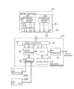
Fig. 2 is a schematic block diagram showing one example
o a home TV gaming machine capable of utilizing the
cartridge as shown in Fig. 1. A configuration in this Fig.
2 shows the above-described "Nintendo Entertainment System"
`' manufactured and sold by the applicant of the present
20 invention. However, note that t~le present Invention can
e.uti-lïze~ for every apparatus s~ucn -as ~-n-e gaming-a-ppa-ra-~as
or a microcomputer ~hat uses an e~ternal memory c-a-rtrr~g-e.
As described above, the cartridge' 10 comprises the
25 program memory 24, the character memory 26 and the
_ 9 _
i' ~B .
` " ~,3,~
semiconductor device 28 which are mounted on the printed
circuit board 18, and the protrudent portion 20 of the
printed circuit board 18 is attached to an edge connector 32
of a gaming machine main unit 30, and thereby the cartridge
5 10 and the gaming machine main unit 30 are connected
electrically so as to constitute one gaming system.
The gaming machine main unit 30 comprises a micro-
processor 34 which may be, for example, the integrated
circuit "2A03" manufactured by Nintendo, and controllers
10 38a and 38b are connected to the microprocessor 34 through
an I/O interface 36. The gaming machine main unit 30 is
fur-ther provided with a PPU tpicture processing unit) 40, a
video R~M 42 and an RF modulator 44. For the PPU 40, for
example, the integrated circuit "2C02" manufactured by
15 Nintendo ls used, and the PPU 40 reads video data under the
control oE the microprocessor 34, and gives the same to the
RF modulator 44 as a video signal. The RF modula-tor 44
outputs a video signal being given as a television signal
for a TV receiver, for example, of the NTSC system.
Here, detailed description is made on correlation among
the program memory 24, the character memory 26 and the
semiconductor device 28 in reference to Fig. 3. For
example, the program memory 24 is composed of a lM-bit
masked ROM, and the character memory 26 is composed of a
25 64K-bit static RAM. Ground terminals G of the program
-- 10 --
, .: , : .
~3~
memory 24 and the character memory 26 are connected to the
ground, and-a predetermined powex supply voltage Vcc is
applied to these memories 24 and 26 through power supply
terminals.
A chip enable terminal CE of the program memory 24 is
connected to the gaming machine main unit 30 (Fig. 2)
through a predetermined terminal (for example, No. 44
terminal) of the edge connector 32. A memory select signal
ROMSEL from the gaming machine main unit 30 is given to the
10 chip enable terminal CE. Furthermore, the program memory
24 has address terminals A0-A16 of 17 bits, and has data
terminals D0-D7 of 8 bits. These address terminals and data
terminals are connected to the gaminy machine main unit 30
through the edge connector 32, and data from predetermined
15 terminals, that is, data from the terminals D0-D2 of the
least significant three bits in this embodlment, is given as
bank selecting data and as three~bit input of the semi-
conductor device, that is, the counter 28.
A chip select terminal CS, the chip enable terminal CE
20 and a write enable terminal WE of the character memory 26
are all connected to the gaming machine main unit 30
through the terminals of the edge connector 32 ~for example,
No. 56 termina], No. 17 terminal and No. 47 terminal). A
read signal XD from the gaming machine main unit 30 i~ given
25 to the chip enable terminal CE through the edge connector
.
~3~
32, and the write signal WE is given to the write enable
terminal WE. Also, the character memory 26 comprises
address terminals A0-A12 of 13 bits and data terminals D0-
D7 of 8 bits. The address terminals A0-A12 are connected to
5 the gaming machine main unit 30 through the edge connector
32. The data terminals D0-D7 are connected likewise to the
gaming machine main unit 30.
Note that one digit of address is indicated by the
hexadecimal notation.
In this embodiment, as shown in Fig. 4, the program
memory 24 is constituted, for example, as a set of memory
banks on a 128K-bit basis. This means that the firs-t memory
or the program memory 24 comprises eight 128K-bit banks
BK0-BK7. These banks BK0-BK7 are defined by addresses
15 "00000~lFFFF".
Also, the second memory or -the character memory 26 is
constituted as a 64K-bit static RAM.
Furthermore, in this embodiment, for the semiconductor
device 28, for example, the integrated circuit "74LS161"
20 manufactured by Texas Instruments is used, and accordingly
the semiconductor device 28 is constituted as a three-bit
counter. A read/write signal R/W from the gaming machine
main unit 30 is given to a load terminal LOAD of the counter
28, and as described above, the data terminals D0-D2 of the
25 least significant three bits of the program memory 2~ are
connec-ted to the load terminal LOAD as a preset input.
Furthermore, -the memory select slgnal ROMSEL from the gaming
machine main unit 30 to the program memory 24 is given to a
clock terminal CK through the edge connector 32.
5 Accordingly, count input is given to the counter 28 every
time when the program memory 24 is selected by the gaming
machine main unit 30, and the counter 28 is incremented ~or
decremented) by that count input.
Output terminals of the counter 28 is of three bits, and
10 the three-bit output is given to the address terminals of
the most significant three bits A16, A15 and A14 of the
program memory 24 -through respective OR gates 46a, 46b and
46c. More specifically, the address terminal (No. 35
terminal) of the yaming machine main unit 30 is connec-ted to
15 one input oE each oE these OR gates 46a, 46b and 46c, and
each output of the corresponding bit of the counter 28 is
given to the other input of each OR gate. Accordingly, for
the program memory 24, the bank thereof is selected
accordlng to the bank selecting data (Eig. 4) in the output
20 of the counter 28. For example, as shown in Fiy. 4, if the
output of the counter 28 is "000", the bank BK0 is selected,
if "001" the bank BKl is selected, if "010" the bank BK2 is
; selected, if "011" the bank BK3 is selected, if "100" the
bank BK4 is selected, if "101" the bank sK5 is selected, if
25 "110" the bank BK6 ls selected, and if '1111" the bank BK7 is
9~
selected, respectively.
The microprocessor 34 of the gaming machine main unit 30
is accessible only to two-bank area of the program memory
24 as the first memory. This means that the microprocessor
5 34 has address spaces for two banks, "8000-FFFF". Among
them, a first address space "C000-FF~F" is allocatQd so as
to access in a fixed fashion always to the ~ank BK7 of the
program memory 24. Then, when an arbitrary bank of the
banks BK0-BK7 of the program memory 24 is selected, a second
10 address space of 64K bits defined by addresses "8000-C000"
is allocated to the address space corresponding to the
selected bank.
; Accordingly, in the banks BK0-BK7 of the first memory
24, the bank selecting data for the bank to be selected next
15 is required to be stored in the last of or halfway that
data. .To be detailed, in the bank ~X7 as a standing area,
the data of the bank to be accessed next by the central
processing unit or the microprocessor 34 is stored, and in
the bank to be read next in such a manner, the selecting
20 data for the still next bank is stored. Then, all the banks
of the program memory 24 can be utilized at an arbitrary
timing by the second address space of the microprocessor 34.
In the operation, the power supply is first turned on in
the state tha~ the cartridge 10 is loaded in the gaming
25 machine main unit 30, and immediately after that or after a
- 14 -
B
~3-~J~
reset switch has been depressed, a read command is outputted
from the microprocessor 34 of the gaming machine main unit
30 through the address terminal A14 thereof (No. 35 terminal
of the edge connector 32). When the address terminal A14
5 goes high, all outputs of the OR gates 46a-46c become high,
and "1" is inputted to all of the address terminals A16-A14
of the most significant three bits of the program memory
24, and accordingly, at this point the microprocessor 34 is
accessible to the standing area, that is, the bank BK7 of
10 the program memory 24.
Then, the program data of the bank BK7 of the program
memory 24 is read and the microprocessor 34 is operated
based on that program data. This means that, at this time,
the microprocessor 34 can address the bank BK7 using the
15 first address space of the addresses "C000-FFFF".
The mi.croprocessor 34 executes a program according to a
program data of the bank BK7 of the program memory 24, and
the bank selecting data for designating a bank of the
proyram memory 24 is set in the first of (or in the last of
20 or halfway) that program data. As described previously, the
bank selecting data selects any one of the banks BKO-BK7 of
the program memory 24 by three bits of "000"-"111".
Then, the bank selecting data from the data terminals
D0-D2 of the lleast significant three bits of the program
25 memory 24 is given as a preset input of the counter 28. On
- 15 -
- \
~3''~
the other hand, -the read/write signal R/W is given to the
counter 28 as a load command of the counter 28 from the
microprocessor 34, and at this time, the signal R/W is given
as the high level, and accordingly in the coun-ter 28, the
5 preset inpu-t thereof is not loaded.
When the read/write signal R/W yoes low level during
execution of -the program, that is, when the load command is
given, the bank selecting data outputted from the data
terminals D0-D2 of theleast significant three bits of the
10 program memory 24 is written to the counter 28. Thereafter,
the microprocessor 34 gives a read signalr that is, changes
the signal R/W to the high level, and accesses to the bank
(Eor example, BK6) selected by the counter 28 using the
second address space as described above.
When the memory select signal ROMSEL from the micro-
processor 34 of the gaming machine main unit 30 is low
levelr the counter 28 and the program memory 24 are enabled.
Then, if the data of the selected bank (for example, BK6) is
character data, a command of transferring the character da-ta
20 to the second memory, that is, the character memory 26 is
outputted.
Then~ according to that transfer command, the write
enable signal WE from the microprocessor 34 is changed to
the low level, and write of the character memory 26 is made
25 possible. Then, thle data of the selected bank (for example,
- 16 -
, . .. ..
- ` -
~3~
BK6) of the program memory 24 are all read in the address
sequenee, and the read eharaeter data are given to the
mieroproeessor 34. The rnieroproeessor 34 gives the
eharaeter data to the PPU 40, and the PPU 40 writes the
5 charaeter data to the eharaeter memory 26 in synchronism
with address designating of the character memory 26.
Thereafter, similarly, according to the bank selecting
data contained in the program data from the program memory
24, any of the banks BK0-BK7 of this program memory 24 is
lO addressed as "8000-C000" of the second address spaee of the
microprocessor 34, and the game progresses based on the
program data of the bank selected at that time and the
eharaeter data of the eharaeter memory 26. Aceordingly, the
eharacter data has only to be written in advance to an
15 arbitrary bank of the proqram memory 24 to be required.
This means that the bank seleeting data is set in advance in
a program data eontained in any of the banks of the program
memory 24, and the data of the bank seleeted by the bank
selecting data is written into the character memory for
20 eharacters 26, and thereby the bank of that character data
has only to be accessed only when required. In order words,
proeessing has only to jump to the required bank during
execution of the program to read the character data at that
time. Then, sueh a bank selecting data can be set
25 arbitrarily by the program, and therefore copying or dubbing
- 17 -
- ~3~ Z
of the cartridge 10 can be prevented effectively.
As in the case with this embodiment, even if the maximum
address space of the microprocessor 34 is relatively small,
all of the banks of the program memory 24 can be selected
5 arbitrarily, and therefore the memory capacity which can be
utilized by the microprocessor 34 can be expanded
apparently. In addition, the present invention can be
utilized -not only for the gaming system but also for the
educational system, being able to have universality.
In addition, in the above-described embodiment, the case
is described where among a plurality of banks BK0-BK7
comprised in the program memory 24, in the bank B~7, data
for transfer-controlling the character data (that is, bank
selecting data, latch command of bank selecting data, write
15 command to the character memory 26 and the like) are
program-set in advance, and a return command is set in
advance in the last address o the bank storing the
character data, and with the progress of the game, based on
the program of the bank BK7, a character data of another
20 bank is controlled to be transferred to the character memory
26. However, the transfer-controlling data may be stored in
several bytes close to the last address of each bank storing
the character data.
Also, in the above-described embodiment, a masked ROM is
25 used for the program memory 24. However, for the program
- 18 -
B
.
-
~3~ %
memory 24, for example, an EPROM or the like can be
utilized, and further any type of memory can be utilized if
it not volatile.
Furthermore, in the embodiment, the character data is
5 written into the character memory 26, but for such data,
besides, video data and the like can be written, and in this
case, the character memory 26 can be utilized also as a so-
called video RAM
~lthough the present invention has been described and
10 illustrated in detail, it is clearly understood that the
same is by way of illustration and example onl~ and is not
to be taken by way of limitation, the spring and scope of
the present invention bein~ lim.ited only by the -terms of the
appended claims.
-- 19 --
, .~ - -