Note: Descriptions are shown in the official language in which they were submitted.
COMPUTATION PROCESSOR COMPRISING SEVERAL
SERIES-CONNECTED STAGES, COMPUTER AND
COMPUTING METHOD USING THE SAID PROCESSOR
BACKGROUND OF THE INVENTION
l. Field of_the Invention
The invention pertains mainly to a computation
processor comprising several series-connected stages, a
computer and a computing method to use the said processor.
2. DescriPtion of the Prior Art
There are elementary processors in the prior art such
as, for example, adders or multipliers which use a
structure with several combinational series-connected
stages. Usually, the combinational stages are
series-connected through registers by which it is possible
to re-synchroni2e the device with a clock. A processor of
this type is called a pipe-line processor.
The time taken to compute a datum for a pipe-line
processor is equal to the time taken to go through all the
series-connected stages. For example, a pipe-line adder
with four stages delivers the sum of two data presented at
its inputs at the end of four clock cycles. Thus, if a
processor of this type is presented with data to be
processed at each clock cycle, the total computing power,
once the process has begun, is equal to the computing power
of each stage of the pipe-line multiplied by the number of
~, ~
~3~
pipe-line stages.
Unfortunately, in practice, it is very rarely possible
to present data for processing to a pip~-line elementary
processor at every clock cycle. Vnder optimum conditions,
it is possible to present a processor of this type with a
long vector, i.e~ with finished sequences of the data to be
processed. The efficiency, namely the computing power of a
processor of this type, decreases very swiftly as and when
the length of the vectors presented to the processor is
diminished. When we approach vectors comprising a single
set of data to be processed, the computing power of the
elementary processor tends towards the computing power of
one stage of the pipe-line.
3. Summary of the Invention
The processor according to the present invention
comprises an elementary processor using several
series-connected pipe-line stages. To avoid the
disadvantages of devices of the prior art, the processor
according to the invention comprises a mode of operation
enabling it to act as n different processors, n being the
number of stages of the pipe-line. Since the n processors
do not exist physically, they will hexeinafter be called
virtual processors. Each independent processor can process
one program independently of the ones processed by the n-l
other virtual processors.
,
The device according to the present invention provides
for the simultaneous execution of several tasks or for the
breakdown of a complication computation into several simple
computations. This facility will be especially appreciated
for computations used in the processing of signals.
Furthermore, the apparent length, for the processor of
the pres~nt invention, of the vectors is equal to n times
the real length. Thus, when short vectors are used, the
computing power of the device according to the present
invention is appreciably greater than that of a
conventional type of device comprising the same number of
stages with the same clock cycle.
The main object of the invention is a computation
processor with n series-connected pipe-line stages,
comprising means capable of supplying, from one memory, n
independent flows of data so as to enable the said
processor to simultaneously perform n computations.
Another object of the invention is a method to perform
computations using a processor with n series-connected
pipe-line stages and a memory, wherein the memory is
organized in n memory pages and wherein, at each clock
cycle, the said processor is capable of having access to a
dif~erent memory page, the change o the memory page being
obtained by circular permutation.
-~ ~.3~
BRIEF DESCRIPTION OF THE DRAWINGS
The invention will be better understood from the
following description and the appended figures, given as
non-exhaustive examples, of which:
Figure 1 is a diagram of a first embodiment of a
processor according to the invention;
- Figure 2 is a timing diagram of the operation of a
processor according to the invention;
- Figure 3 is a diagram of a scecond embodiment of a
processor according to the invention;
- Figure 4 is a timing diagram of the operation of the
processor of figure 3;
- Figure 5 is a third example of an embodiment of the
processor according to the invention;
_ Figure 6 is an explanatory diagram of data
transfers;
- Figure 7 is a diagram illustrating the external
communications device of the processor according to the
invention;
~ Figure 8 is a diagram of the external communications
device according to the invention;
- Figure 9 is a diagram illustrating an association of
processors according to the invention;
- Figure 10 is a diagram illustrating an association
of processors according to the invention;
.
3-3~
- Figure 11 is a fourth alternative embodiment of the
processor according to the invention.
Figures 1 to 11 use the same reference to designate
the same elements.
In the timing diagrams, the same references are used
to designate the pulses and clock cycles.
DESCRIPTION OF THE PREFERRED EMBODIMENTS
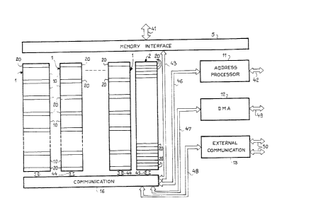
Figure 1 shows a computing processor comprising at
least one elementary processor 1 with several series-placed
pipe-line stages 10. The processor further comprises a
memory interface 5 and an address interface 11.
Advantageously, the processor has a bank 2 of registers 20.
Each pipe-line elementary processor consists of a
succession of registers 20 and combinational parts 10. The
elementary processors 1 are, for example,
adders/multipliers, arithmetic and logic units (ALU),
accumulating multipliers or microprocessors. When the
processor according to the invention is being designed,
depending on the computations that are sought to be made,
the said processor is made with the necessary elementary
processors. It is possible to use several elementary
processors 1 of the same type.
The address processor 11 makes it possible, by
addressing an external memory, to give the elementary
processors 1 the data to be pxocessed. The random-access
~3~f ~ f~
memory is organized in m memory pages corresponding to n
virtual processors made by the processor according to the
invention. The address processor 11 gives, successively,
through an address bus 42;
- The address of the first datum of the first virtual
processor;
- The address of the first datum of the second virtual
processor;
- The address of the first datum of the third virtual
processor;
*
*
*
- The address of the first datum of the ith
virtual processor;
*
*
*
- The address of the first datum of the nth
virtual processor;
- The address of the second datum of the nth
virtual processor;
- The address of the second da~um of the second
virtual pro~essor
~3~
*
*
*
- The address of the second datum of the nth
virtual processor;
~ The address of the third datum of the first virtual
processor;
- The address of the third datum of ~he third virtual
processor,et c.
In this way, the computing processor of the present
invention has high computing power even in the presence of
short vectors to be processed. The random-access memory
shown in figure 1 gives the the elementary processors 1
data needed for the desired processing operation, through a
lS bus 41 and the interface 5. For example, the memory (not
shown) gi.ves two data per adder and per multiplier.
In one embodiment of the device according to the
invention, the processor comprises a communications device
16 with which to select the elementary processor or
processors connected to the interface 5. Advantageously,
the communications device 16 can be used for the exchange
of information among the elementary processor 1I the
register bank 2 and the address processor 11. The
elementary processors 1 are connected to the communications
device 16 by means of the buses 44. The bank 2 of registers
13~
is connected to the communications device 16 by means of
a bus 45. The address processor is connected to the
communications device 16 by menas of a bus 46. The memory
interface 5 is connected to the communications device 16 by
means of a bus 43.
Advantageously, the processor according to the
preseent invention has a direct memory access processor 12
(DMA). The direct memory access processor makes it possible
to read and write in the memory assigned to the processor
of the invention while the said processor performs
computations. The direct memory access processor 12 is
connected by a bus 47 to the communications device 16 and
by bus 49 to the random access memories.
Advantageously, the device according to the preseent
invention has an external comminications device 15. For
example, the external communications device 15 is an
interface with at least one bus 50 used to exchange data
with the exterior, for example with other identical
processors. The external communications device 15 is
connected by a bus ~8 to the communcations device 16.
Figure 2 shows the timing diagram of the operation of
a processor according to the invention, comprising four
pipeline stages. The four pipeline stages correspond, for
example, to four registers connected by three combinational
parts.
The processor is synchronized by a clock HE, the
pulses 29 of which are evenly spread out in time. A full
computing cycle CC therefore lasts four clock cycles 29. In
figure 2 , a computing cycle CC starts at the third clock
pulse 29. This corresponds to the beginning of the
computation by the first virtual elementary processor
PEVi. The duration 36 needed for the computation is
equal to four clock cycles 29. Thus, the first virtual
elementary processor will deliver its pulse at the seventh
clock pulse 29.
The computation of the second virtual elementary
processor PEVi+l starts at one clock pulse 29 after the
beginning of the computation by the virtual elementary
processor PEVi, namely, in the example of figure 2, at
the fourth clock pulse 29. This computation will be
completed at the eighth clock pulse 29 (not shown).
The computation of the third virtuel elementary
processor PEVi~2 starts at the fifth clock pulse 29.
This computation ends at the ninth clock pulse 29 (not
shown).
The computation of the fourth virtuel element~ry
processor PEVi+3 starts at the sixth clock pulse 29.
This computation ends at the tenth clock pulse 29 (not
shown in figure 2).
The computation of the first virtuel elementary
.
processor PEVi starts at the seventh clock pulse 29.
This computation ends at the eleventh clock pulse 29 (not
shown in figure 2).
Thus, although a computation period 36 lasts four
clock cycles, a result is delivered by one of the virtual
elementary processors at each clock pulse 29.
Figure 3 shows an embodiment of a processsr 100
according to the invention. For the clarity of the figure,
only the data buses have been shown. The embodiment of the
processor 100 according to the invention, shown in figure
3, comprises an arithmetic and logic unit 13, a multiplier
14, a register bank 2. A communications device 16 is used
to urnish data needed for computations to the inputs of
the arithmetic and logic unit 13, the multiplier 14 and the
register bank 2. Similarly, the communications device 16
can be used to collect the results of the computations by
the arlthmetic and logic units 13 and the multiplier 14 as
well as to read the data stored in the registers 2 of the
register bank 2. Furthermore, the communications device 16
is connected by a bi-directional bus 43 to the memory
interface 5, a bus 52 to a device (not shown), which is
capable of giving constants needed for the computationsl
and to the external communications devices 15 by a
bi-directional bus 48. The external communications device
is, for example, a communications interface by which
. , .
~3~
several processors 100 according to the invention, can be
connected in rings. For example, each processor 100 is
connec~ed to its neighbour on the right and on the left.
The information can spread from one processor to the next
one until it reaches the processor for which it is
intended. A device of this type is described in the Frech
patent No. 83 15649.
The processor 100 according to the present invention
advantageously comprises a direct memory access circuit 12,
an address processor 11. A memory interface 5 provides
access to a random-access memory (RAM) 3. The memory 3
advantageously consists of two memory banks connected by
buses 41 to the interface 5. Each memory bank is
advantageously divided into memory pages, the total number
of memory pa~es being advantageously equal to the number of
virtual processors equivalent to the processor 100. In the
example shown in figure 3, since the processor 100 is e~ual
to four virtual processors, each memory ban~ 3 comprises
two memory pages, 30 and 32 on the one hand and 31 and 33
on the other~
To make it possible to access a datum in memor~ 3, the
address processor 11 transmits the address of the datum to
be read through the address bus (not shown). The datum is
transmitted through the bus 41 to the memory interface 5,
and then from the memory interface 5, through the buses 43
3~
to the communications device 16. The communications device
16 transmits the datum to the arithmetic and logic unit 13,
the multiplier 14, one of the registers 20 of the register
bank 2 and/or the external communications device 15.
The memory interface 5 is furthermore connected to an
input/output bus 51.
The direct memory access device 12 can be used to read
or write in the memory 3, through the bus 51 of the memory
interface 5, without going through the communications
device 16. The division of the random-access memory 3 into
two memory banks provides for direct memory accessing in a
memory bank while the other memory bank is exchanging
information through the communications device 16, or for
two simultaneous memory access operations through the
processor 100 followed by two direct memory access
operatlons .
Figure 4 shows a timing diagram of the functioning of
the processor oE figure 3. The clock pulses 29 correspond
to the crossing of a pipeline stage. At every four clock
pulses 29, a clock pulse 28 is emitted corresponding to a
full computing cycle. During the first clock pulse 29, the
first virtual .elementary processor PEVl accesses the
data 34 through the communications device 16. During the
following three clock pulses 29, the first virtual
elementary processor PEVl performs a computation 35. At
-
~3~
the fifth clock pulse 29, corresponding to the second clock
pulse 28, the first virtual elementary processor PEVl,
having begun a new computation cycl~, again accesses the
data 34 by means of the communications device 16. During
S the following three clock cycles 29 ending the second clock
cycle 28, the virtual elementary processor 1 ends the
second computation.
During the second clock cycle 29 of the first clock
cycle 28, the second virtual elementary processor PEV2
accesses the data 34 through the communications device 16.
During the following three clock cycles 29, the second
virtual elementary processor PEV2 performs the
computations 35. The full cycle of computations by the
second virtual elementary processor ends at the second
clock pulse 29 of the second clock cycle 28. During the
second clock cycle 29 of the second clock cycle 28, the
second virtual elementary processor PEV2, having begun
a new computing cycle, accesses the data 34 by means of the
communications device 16, and so on.
During the third clock cycle 29 of the f.irst clock
cycle 28, the third virtual elementary processor PEV3
accesses the data 34 through the communications device 16.
During the following three clock cycles 29, the third
virtual elementary processor PEV3 performs the
computations 35. At the end of the computing cycle, at the
third clock pulse 29, of the second clock cycle 28, the
third virtual elementary processor PEV3 accesses the
data 34 corresponding to the following cycle and so on.
During the fourth cloc~ cycle 29 of the first clock
cycle 28, the fourth virtual elementary processor PEV4
accesses the data 34 through the communications device 16.
During th~ following three clock cycles 29, the fourth
virtual elementary processor PEV4 performs the
computations 35, During the fourth clock cycle 29 of the
second clock cycle 28, the fourth virtual, elementary
processor PEV4 accesses the data 34 through the
communications device 15 and so on.
As shown in figure 4, the communications device 1~ can
be used for the permanent transmission of data to the
various virtual elementary processors.
Figure 5 shows the transmission of data applied in an
embodiment of the processor according to the invention. The
communications device 16 is connected to two inputs of the
arithmetic and logic unit 13, two inputs of the multiplier
14, one input of the external communications device 15, two
inputs of the bank 2 of the register 20, one input of the
memory interface 5, one output of the memory interface 5,
on~ output of the constant bus 52, one output of the
arithmetic and logic unit 13, one output of the multiplier
14r two outputs of the bank 2 of the register 20, one
14
output of the external communications device 15. The dots
160 represent the connections allowed inside the
communications device 16. The communications device 16,
depending on the instructions that it receives, provides
for the various interconnections desired. In one
embodiment, the communications device 16 comprises
multiplexers. In the example shown in figure 5, the
communications device has eight multiplexers, 7 towards 1,
i.e. with the ability to select one out of 7 possible
outputs.
The communications device 16 thus enables the
processor of the invention to perform several desired
computations. The instructions concerning the
interconnections to be made are received either from a
program memory or from a sequencer (both not shown). The
address processor 11 is connected to the bus 41 which
connects the memory interface 5 with the memory 3. The
address processor 11 is connected by an address bus 131 to
the random-access memory 3.
In figure 6, a timing diagram, pertaining to the
transfers of data read or to be written in the memory 3, is
superimposed on a timing diagram pertaining to the
transfers of data fxom the bank 2 of registers 20. In the
example shown in figure 6, only the exchanges, as regards
the bank 2 of registers 20 and the communications device
3~
16, done for the first virtual elementary processor
PEVl have been shown. Figure 6 shows the exchanges
between the bank of registers 2, an example of the
random-access memory capable of performing one read and one
write operation per clock cycle 29 through the
communications device 16~ The device according to the
present invention comprises registers 20 used to
synchronize the flows of data intended for the virtual
elementary processors. The numbering of the virtual
elementary processor indicates the virtual elementary
processor for which the communications device 16 works. The
random-access memory 3 is divided into two memory banks.
At the second clock pulse 29, we have two data
transfers for writing 291 between the communications device
16 and the register bank 2.
At the second clock pulse 28 we have one data transfer
for writing 293 between the communications device 16 and
the memory interface 5, the reading being done between the
; fourth and fifth pulses 29.
At the third clock pulse 29, we have a data transfer
for writing 293 between the communications device 16 and
tha memory interface 5.
At the fourth clock pulse 29, we have a data transfer
for writing 293 between the communicaton devices and the
memory interface 5.
16
~3~ 4
At the fifth clock pulse 29, corresponding to the
second clock pulse 28, we have a data transfer for writing
293 between the communications device 16 and the memory
interface 5.
At the fifth clock pulse 29, corresponding to the
second clock pulse 28, there is a data transfer after
reading 294 between the memory 3 and the communications
device 160
At the fifth clock pulse 29, corresponding to the
second clock pulse 28, there are two data transfers after
reading 292 between the register bank 2 and the
communications device 16.
At the sixth clock pulse 29, there is a transfer of
data after reading 294 between the random-access memory 3
and the communications device 16.
At the seventh clock pulse 29, there is a data
transfer after reading 294 between the random-access memory
3 and the communications device 16.
At the eighth clock pulse 29, there is a data transfer
after reading 294 between the random-access memory 3 and
the communications device 16.
Thus, overall, in the case of the use of a bank 2 of
registers 20 comprising two physical doors and one double
~ank of random-access memories 3, two write operations and
two read operations are performed per clock cycle 28 and
per virtual elementary processor, as well as one read
operation and one write operation in the memory 3 per the
clock cycle 28 by a virtual processor.
Thus, four completely independent data flows are
obtained in the processor. The use of two memory 3 banks
provides simultaneous memory accessing for the first and
second virtual elementary processors PEVl and PEV2,
and then for the third and fourth elementary processors,
PEV3 and PEV4.
Although the use of the memories 3 provides for only
one access per clock cycle 29, the said use does not go
beyond the scope of the present invention.
Figure 7 shows an external com~unications device 15.
The device is connected, not only to the bus 48 which
connects it to the communications device 16 and the two
data exchan~e buses 50, but also to two control buses 54
and 55. q`he control bus S~ is, for example, a six-bit bus
and the control bus 55 is a three-bit bus. The control
buses 54 and 55 are used to handle exchanyes among the
processors 100 aaccording to the invention. Since the data
is transmitted from one processor to the next, it is
imperative that the unavailability of one of the processors
should not prevent the ring-connected bus 50 from
functioning. On receiving a command, the external
communications device transmits the data, short-circuiting
18
~3~
the processor 100 to which the said external communications
device belongs.
Figure 8 shows a functional diagram of the external
communications device 15, corresponding to a virtual
processor. The device comprises a first multiplexer 63 with
three inputs and one output. A first input comes from a
first hus 50. A second input comes from a second bus 50.
The third input of the multiplexer 63 comes from the input
of the bus 48. Advantageously, the bus 48 comprises a
synchronizing register 62 which synchronizes the clock
pulses 28.
Furthermore, the output of the register 62 is
connected to the multiplexer with three inputs as well as
to two multiplexers with two i.nputs and one output 63.
Advantageously, the output of the multiplexer 63 with three
inputs is connected to the bus 48 by means of a register
62. The output o the register 62 is connected firstly, to
the bus 48 and, secondlyr to second inputs of two
multiplexers 63 with two inputs. The output of each of the
multiplexers with two successive inputs is connected to
three-state operators 64. The three-state operators 64 make
it possible to obtain, in addition to the low logic state
and the high logic state, a third logic state with an
infinite output impedance by which it is possible to
; 25 isolate the external communications device 15 from the
19
, . .- . .
buses. The change-over to infinite impedance is done, for
example, by a control Ç5.
Figuxe 9 shows a set of processors 100 according to
the invention. Each processor 100 has a dedicated
random-access memory 3. For example, each processor 100 has
a double memory bank 3 connected by buses 41. A complete
computer comprises, for example, sixteen processors 100
according to the invention. For the clarity of the figure,
only three processors have been shown. The processors 100
are connected by a ring-connected bus 50. This bus is
furthermore connected to a program sequencer 502. The
program sequencer 502 makes it possible to control the
processors 100 through a bus 501. B~ addressing the same
command to all the processors 100, a parallel computer
lS (single instruction multiple data stream or SIMD machine)
is made. In one embodiment comprising a sequencer 502,
capable of addressing different commands to the various
processors 100, a multiple instruction multiple data stream
(MIMD) machine is made. Advantageously, the program
sequencer 502 is connected to a memory sequencer 504. The
memory of the program is not shown in figure 10. In the
example shown in figure 9, the input-output buses 51 of the
processors 100 are connected to a single bus 505, capa~le
of making transmissions sequentiallyr
~igure 10 shows a computer according to the present
invention comprising several processors 100. In the
alternative embodiment of figure 11, the input/output buses
51 of the processors 100 are connected to parallel
communications channels. Thus, it is possible to make
exchanges conskantly with all the memories of all the
processors 100.
Figure 11 shows an example of a processor 100
according to the invention, capable of working
autonomously. This processor 100 comprises, in addition to
the elements shown in figures 1, 3 and 5, a memory
sequencer 504 connected to the memory 3 by a bus 520 and a
program sequencer 502 connected by a control bus 501 to the
arithmetic and logic unit 13, the multiplier 14, the
communcations device 16, the external communications
devices 15 and the interface 5.
The invention applies to the making of computers with
high computing power. The invention applies especally to
the digital processing of signals.
21