Note: Descriptions are shown in the official language in which they were submitted.
~L3~9~
ELECTRON BEAM ADDRESSED LIQUID CRYSTAL LIGHT VALVE
1 BACKGRO~ND OF ~E_INVENTION
Field o~ the Invention
This invention relates to liquid crystal light valves
which modulate readout optical beam in response to an
input electrical beam pattern.
Descri~tion o~_the Prior Art
Liquid crystal light valves (LCLVs) generally employ
twisted nematlc liquid crystal cells in which the liquid
crystal molecules are ordered such that plane-polarized
lighk passing through the cell is rotated 90. When
sufficient voltages are applied to particular areas of the
cell, the mol~cular axes o~ th~ liquid crystal molecules
in these axeas oriant themselves parallel to the applied
electric ~ield. Polarized light can then pass ~hrough
thesQ areas of the cell e~senti~lly unchanged, while light
is block~d in ~he areas o~ the liquid crystal to which no
field is applied. Optical images can thus be produced by
the spatial voltage pattern applied to the device.
Past implementations of LCLVs have included devices
that are laser address~d, and devices that are photo-
conductor coupled to a cathodQ ray tube (CRT) or other
light source. Laser-addressed systems, while exhibiting
high resolution, are storage devices that may require
several seconds to ~ill the screenl and use ge~erally
complex optical systems for both addressing and projec-
tion. Photoconductor-coupled devices, in addition to the
.
~3~
addressing optics, have used either multilayer construc-
tion to isolate the projection and addressing light, or
have severe constraints on the wavelength of the
addressing/projection light.
An electron-beam addressed LCLV could, at least
conceptually, eliminate prior problems associated with
photoconductors and light blocking layers. In addition,
such a device could be made sufficiently fast for
real-time operation. The most current electron-beam
addressed LCLV prior to the present invention is a
Tektronix Corp. device described in an article by Duane
A. Haven, "Electron-Beam Addressed Liquid-Crystal Light
Valve", IEEE Transactions on Electron Devices, Vol.
ED-30, No. 5, May 1983, pages 489-492. This article
describes an LCLV device in which electrons form a
writing gun impinge upon a target electrode, and are
subsequently erased from the target by means of flood
guns. l'he flood yuns recharge the target electrode to a
controlled uniform potential. One problem associated
with this device is that flood guns are not uniform,
and produce a non-uniform distribution of electrons on
the target electrode. This in turn produces an image
that is not uni~orm. Image retention is another
problem. The low energy ~lood gun is not capable of
totally erasing the image created by the deep implant of
electrons by the high energy writing gun. The Tektronix
device requires the use of an expensive transmissive
CRT, and its optically transmissive nature limits the
choice of materials that can be used in connection with
the LCLV. Some materials which might otherwise be
suitable are birefringent and can rotate the
polarization of the read-out light, and therefore are
not suitable. It would also be desirable to increase
the sensitivity of the device.
~''
,.
..,, ~
~ , ~
9~
SUMMARY OF THE INVENTION
In view of the above problems associated with the
prior art, it is an object of an aspect of the present
invention to provide a novel and improved electron beam
addressed LCLV which is simple in construction, has a
high resolution display, avoids the need for a flood
beam and its attendant image distortion, does not
suffer from the image retention problem, and does not
require a high transmissive membraneO
An object of an aspect of the invention is the
provision of such an electron be~m addressed LCLV which
is less expensive, and yet more sensitive, than prior
devices.
These and other objects are accomplished in the
present invention by an LCLV which is designed to
operate primarily in a reflective mode. A flat,
electrically resistive membrane is positioned on the
opposite side of a liquid crystal layer from the readout
optical beam, with a layer of partially conductive
material supported on the membrane and adapted to be
addres~ed by the electron beam. An accumulation of
electric charge at any location in the partially
conductive material, due to the impinging electron
beam, produces a voltage across a correspondi~g location
in the liquid arystal. The liquid crystal voltage
controls its light transmitting or polarization
rotation characteristics as desired. A charge
collection means, preferably in the form of a conductive
matrix grid, is disposed on the partially conductive
layer to collect charge received by that layer from
electron beam scanning. The grid divides the partially -
conductive layer into a series of pixels, with the
matrix material surrounding each pixel on the electron
beam side of the partially conductive layer. A voltage
of one polarity i5 induced across the corresponding
location of the liquid crystal layer in response to the
, . .
electron beam impinging upon a pixel in the partially
conductive layer. Charge then dissipates from the
pixel into the surrounding grid at a rate which is fast
enough to substantially discharge the pixel during the
interval between electron beam scans, but is slow enough
to produce an image for a readout optical beam. A
circuit means is conne ted to dissipate the charge
received by the conductive matrix from the partially
conductive layer. The resistances and capacitances of
the liquid crystal layer, the membrane and the partially
conductive layer ara selected to produce a substantially
AC voltage across the liquid crystal during the
conductive layer discharge following each electron beam
scan. The pixels are thus automatically erased without
the need for flood guns.
In the preferred embodiment a mirror is disposed on
the opposite side of the liquid crystal layer from the
readout beam, and reflects the readout beam back through
the liquid crystal. A transparent electrode i5 provided
on the readout beam side of the liquid crystal, and is
connected to provide a voltage reference for the liquid
crystal. The conductive matrix and transparent
electrode may either be grounded, or connected by means
of an AC power supply which improves the liquid crystal
sensitivity.
Other aspects of this invention are as follows:
A liquid crystal light valve (LCLV) adapted to be
addressed by a scanning electron beam, comprising:
a liquid crystal layer adapted to be addressed by a
readout optical beam,
a flat electrically resistive membrane supported in
proximity to the liquid crystal layer on the opposite
side thereof from the readout beam,
a layer of partially conductive material supported
by the membrane and adapted to be addressed by the
alectron beam, the accumulation of electric charge in
'
~3~?~97~
4a
the partially conductive material from the electron
beam producing a voltage across the liquid crystal,
means for collecting charge received by the
partially conductive layer as a result of electron beam
scanning of that layer, and
circuit means connected to dissipate charge
received by the collecting means from the partially
conductive layer,
the resistance of at least one of the liquid
crystal light valve layers being high enough to produce
a substantially AC voltage across the liquid crystal
following each electron beam scan.
A liquid crystal light valve (LCLV) adapted to be
addressed by a scanning electron beam, comprising:
a li.quid crystal layer adapted to be addressed by a
readout optical beam,
a layex of partially conductive material supported
in proximity to the liquid crystal layer on the
opposite side thereof from the electron beam, and
adapted to be addressed by the readout beam, the
accumulation of eleatrons in the partially conductive
layer from an electron beam scan produci.ng a voltage
across the liquid crystal,
a grid of conductive material disposed on the
partially conductive layer and adapted to receive
electron leakage from the partially conductive layer,
the grid dividing the partially conductive layer into a
series of pixel elements with grid material surrounding
the pixel e].ements to receive electron leakage0 therefrom, and
circuit means connected to discharge the grid of
electrons leaked from the partially conductive layer !
the dimensions and materials for the various
elements being selected, relative to the electron beam
scanning rate, to produce an electron leakage rate from
the partially conductive layer pixels into the grid that
is fast enough to substantially dissipate electrons
~3C~
4b
delivered to the pixels during an electron beam scan
prior to the next scan, but slow enough for the liquid
crystal to produce an image for a readout beam.
A liquid crystal light valve (LCLV) adapted to be
addressed by a scanning electron beam, comprising:
a liquid crystal layer adapted to be addressed by a
readout optical beam,
a flat, electrically rr-sistive membrane supported
in proximlty to the liquid crystal layer on the opposite
side thereof from the readout beam,
a layer of partially conductive material supported
by the membrane and adapted to be addressed by the
electron beam,
a conductive grid disposed on the partially
conductive layer and dividing that layer into pixel
elements, the conductive grid being adapted to receive
electrical charge from the partially conductive layer
pixel elements, and
circuit means connected to dissipate charge
received by the grid from the partially conductive layer
as a result of electron beam scanning of that layer,
the accumulation of electric charge in the
partially conductive material due to an electron beam
scan and the subsequent dissipation of the charge
through the grid producing a voltage across the liquid
crystal and a related liquid crystal current ILC in the
form:
LC ~LC 5l-52 ( l 2
~hore 1,2 2rMrLC ( ~ ~C ~ C ) M LC)
RMC~, rLC = CL~RLC, T _ R C
,
~3~
4c
CLc = liquid crystal capacitance per pixel
RLC = liquid crystal resistance per pixel
CM = combined membrane partially conductive layer
capacitance per pixel
~ = effective combined membrane partially
conductive layer sheet resistivity per pixel,
CLc, RLC, CM and RM being selected to produce an
AC voltage across the liquid crystal during a
substantial portion of the time between the electron
beam scans.
Other features and advantages of the invention will
be apparent to those skilled in the art from the
following detailed description of preferred embodiments,
taken together with the accompanying drawings, in which:
DESCRIPTION OF THE DRAWINGS
FIG. 1 is a sectional view of an electron beam
addressed LCLV constructed in accordance with the
present invention;
FIG. 2 is a fragmentary elevation view of a portion
of the conductive matrix used to dissipate charge
received from the electron beam;
FIG. 3 is a graph illustrating the time-based
voltage signal established at a particular liquid
crystal pixel location in response to an electron beam;
: 25 FIG. 4 is an equivalent circuit of the LCLV
~ elements governing the charge dissipation; and
._ r
~3~:1197~
1 FIG. 5 is an elevation view of the back face of the
LCLV which uses a peripheral conductive ~ing to dissipate
signal charge.
5 DETAIL~D DESCRIPTION OF PREFERRED E~MBODIMENTS
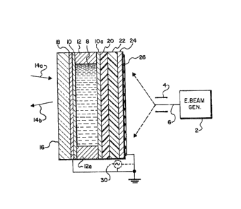
Referring to FIG. l, a modified form of an LCLV is
~hown which provides a high resolution display of an
electron beam scan pattern. A CRT is represented as an
electron beam generator 2 and a pair of deflection plates
4 which cause the beam 6 to scan in a raster pattern. An
additisnal pair of plates would also be provided to con-
trol the beam scan into and out of the page. The beam
current is typically in the approximate range of 10 micro-
amp~ to l milliamp.
The LCLV includes a layer of liquid crystal 8 which
is enclosed in a cell ~ormed by insulating films 10 and
lOa on eithex side to facilitate the liquid crystal align-
ment and to provide chemical isolation, and spacers 12 and
12a which maintain a suitable gap between insulating films
10 and lOa and preveslt liquid crystal 8 ~rom escaping.
The le~t side of the LCLV is re~erred to as the
"readout" side, since an optical readou~ beam 14a is
directed onto th~ valve from this side and is reflected as
an output beam 14b after it has been modulated in accor-
danca with the electron beam pattern. ~ transparent coverplate 16, pre~erably made form glass, cover~ and prote~ts
the left hand sida of the device. A transparent electrode
18, preferably formed from tinindium oxide, is coated on
the inner face of cover plate 16. This electrode provides
a reference for the voltage established across the liquid
crystal, as described below.
A mirror 20 is provided on the opposite side of the
liquid crystal cell from the readout beam. This mirror
receives the readout beam~ and reflects it back again
through the liquid crystal. It can be implemented with a
conventional wide band, high reflectivity dielectric
., ~
13G1971
mirror. This is in contrast to many light valves, which
employ a photoconductive layer; these require the mirror
to have a modified dielectric, since the mirror is required
to absorb almost all of the readout light which is not
reflected so as to avoid rendering the photoconductive
layer conductive. The present light valve, however,
does not employ a photoconductive layer, and therefore
the mirror can be much simpler. Instead of a dielectric
mirror, a metal matrix mirror such as that disclosed in
U.S. Patent No. 4,973,136, issued November 27, 1990,
assigned to Hughes Aircraft Company, the assignee of the
present invention, may also be employed.
A support membrane 22 is positioned on the electron
beam side of mirror 20, and supports both the mirror and
a layer of partially conductive material 24. The membrane
should be resistive so as to avoid shorting the deposited
charge image, with a high sheet resistivity in the order
of 1012 ohms/sq. or greater. It is either rigid, or
stretchable so that it can be formed with a very flat
surface plane; an outer ring (not shown) may be provided
as a base for stretching the membrane. Suitable mem-
brane materials are Kapton, mica and boron nitride.
To protect it from possible electron damage, the membrane
might incorporate a thin layer of sio2 or other res.istive
material 24 evaporated onto its electron beam side.
A matrix of conductive material 26, preferably in
the form of a metallic grid as illustrated in FIG. 2,
is deposited on the outer face of the partially con-
ductive layer 24. Each of the grid openings 28 defines
a pixel for purposes of forming an image from the scan-
ning electron beam. The grid 26 and the electrode 18
are connected together to ground, or, in another embod-
iment, an AC voltage source 30 may be connected between
these two elem~nts as descr;hP~ below. The dimensions of
the grid and underlying Fartiall~ conducti~e layer, and the
conductivity of the partially conductive layer, are selected so
,~
~L3V~7~
1 that electrons absorbed within each pixel of the partially
conductive layer during a particular scan will leak out
through the grid by the time the electron beam has fin-
ished a scanning cycle and returned to that pixel. For a
television scan rate 30-60 Hz, the leakage rate should be
fast enough to dissipate the pixel in the approximately
17-30 milliseconds between scans. ~ow~ver, the dissipa-
tion through the partially conductive layer should be slow
enough 50 that an image is left for the readout beam 14a
to observe. The bulk resistance o~ the partially conduc-
tive layer is preferably within the range of about 101-
10l3 ohms per square and its thickness is preferably about
3-10 microns; the resistivity may be in the order of 107-
101 ohm cm. Suitable partially conductive ma~erials
include silicon dioxide and cryolite; cadmium telluride
may be acceptable in some applications, but ~or others it
may be too conductive. Typical pixel sizes are 0.01-0.15
mm. per side.
The electron charge absorbed into any particular
pixel o~ the partially conductive layer 24 as a result of
the electron beam scan produces a voltage across a corre-
sponding location o~ the li~uid crystal. Since the vari-
ous elements of the light valve have a high resistance to
lateral spreading, an essentially 1:1 correspondence can
be achieved between the individual pixel areas of the
partially conducti~e layer which receive electron charges,
and corresponding areas of the liquid crystal which sup-
port a voltage determined by the absorbed charge. To
avoid an excessive voltage drop across the membrane at the
expense of the liquid crystal volt~ge, the membrane should
be made very thin, in the order of about 4-12 microns.
If one of the layer in the sandwich, for instance the
mirror or the membrane or both, is a good insulator, the
pixel voltages established across the liquid crystal from
an electron beam scan will be AC rather than DC. An AC
operation is a distinct advantage, since liquid crystal
~,~
~3~97~
1 tends to decompose under sustained DC operation. The
liquid crystal polarization shift responds to the RMS
voltage level, so that an AC voltage may be used to estab-
lish the polarization shift without the decomposition
effects of DC operation. The AC voltage effect on the
liquid crystal an electron beam scanning a pixel on the
partially conductive layer is illustrated in FIGo 3 ~ in
which the liquid crystal voltage at the pixel location is
plotted against time. The beam scans across the crystal
in a very short pe.riod of time, rapidly depositing elec-
trons which produce a negativ~ voltage peak 32 across the
liquid crystal. The electron beam will typically deposit
charge onto a pixel in the order of 30 nsec. A~ter the
beam has passed, the electrons absorbed into the pixel
will begin to ~low back out to the right towards the
metallic grid 26. The conductive grid material surround-
ing each grid opening 28 ~FIG. 2) will attract the excess
electrons within the surrounded partially conductive layer
pix91; these electrons are dissipated to ground. The
outflow of electrons form the partially conduc~ive layer
24 into the conductlve grid is illustrated by electron
flow lines 34 for one pixel in FIG. ~ AC power supply 30
can bs used to bias the liquid crystal to a voltage near
its threshold voltage, so as to improve its sensitivity.
Returning to FIG. 3, after the electron beam has
passed the pixel and a maximum negative voltage produced
across the liquid crystal, the liquid c~ystal voltage
gradually decays along line 3~. As electrons from the
partially conductive layer 24 continue to flow out to the
grid 26 in the opposite direction to the original beam
electrons, the liquid crystal voltage becomes positive,
crossing the zero voltage axis at point 38. It thereafter
- reaches a positive voltage peak, which is significantly
less than the initial negative voltage peak, and decays to
zero as the excess charge in the partially conductive
layer dissipates.
13~9~L
1 If at least one of the light valve layers is a good
insulator, the area under the negative portion of the
liquid crystal voltage curve will generally be equal to
the area under the positive portion of the curve. The
voltage decays back essentially to zero during the inter-
val betwPen successive ele~tron beam scans, rasulting in
an AC li~uid crystal voltage characteristic over the
course of repeated beam scans. This avoids the deteriora-
tion problem associated with DC operation, which was
discussed above. On the other hand, the voltage decay is
slow enough so that the liquid crystal has ~nough time to
respond and produce the desired image.
An equivalent circuit for the charge dissipakion from
the partially conductive layer is illustrated in F~G. 4.
V(t) represents the voltage at the liquid crystal/membrane
interface resulting from the chaxge Q deposited in a
particular pixel by the electron beam, ~LC and CLC are
respectively the resistance and capaaitance of the liquid
crystal, CM is the co~bined parallel capacitance of the
membrane and partially conductive layer, and RM is the
combined parallel effective sheet resistivity of the
membrane and partially conductive layer, all for one pixel
element. The membrane and partially conductive layer
capacitances are gen~rally of the same order o~ magnitude,
wherea~ the membrane sheet resistivity is generally much
greater than that of the partially conductive layer.
Therefore, the membrane and partially conductive layer
capacitances will each materially contribute to CM, while
the membrane resistivity can generally be lgnor~d. The
charge deposited by the electron beam can flow out to the
grid potential either directly through the partially
conductive layer, or through a parallel path consisting of
the bulk of the membrane and liquid crystal to elec~rode
18. The expression ~or the liquid crystal current result-
ing from V(t) can be shown to be:
~3r~9~
I-C rLC Sl-52 (Sle -52e 2 )
wher~ Sl ,2 2TM7LC ( M rLc ;-\/(TM~T~C~T)2-4rMT~C)
M RMCM ~ T~C ~ CLcRLc, T = RLcCM
An AC voltage curve such as that shown in FIG. 3 will
result from the following set o~ values, among others:
RLC = 6xlOll ohms
RM = 1012 ohms/sq.
CLC = SX1O-1S farads
CM = 6X10-l~ farads
IBF,AM = 100 microamps
A very important and novel feature of this arrange-
ment is that, beginning with a basically single polarity
electron beam, an AC voltage is produced across the liquid
crystal. Another advantage is the achievement of a very
high resolution. With-an electron beam diameter of 0.025
m~. and a 5 cm. light valve, a 2,000 line system can be
attained. The device has a VQrY fast response time, being
limited principally only by the liquid crystal~ It aleo
has a very simple ~tructure that eliminates the need for
fiber optics coupling plates or inpu~ imaging lenses used
with prior devices. An image is produced with a high
degree of uni~ormity, since each pixel o~ the partially
conductive layer discharges directly into the adjacent
conductive grid. It is also considerably more sensitive
than the prior Tektronix or similar devices - since the
present light valve is reflective rather than transmis-
sive, the readout beam passes through the liquid crystal
twice, both before and af~er reflection. This will permit
a thinner liquid crystal layer to be used for the same
sensitivity, or conversely will produce a greater sensiti-
vity for the same liquid srystal thickness. Since the
liquid crystal response time varies with the square of its
:
~L3~9~L
11
1 thickness, any reduction in thickness will have a very
positive effect upon response time.
In fabricating the device shown in FIG. 1, the mirror
20 i5 deposited onto the membrane 22 in one deposition
run, and the partially conductivP layer 24 is deposited
onto the membrane in a separate deposition run. It would
also be possible to reverse the positions of the membrane
and mirror, so that the mirror is sandwiched between the
membrane and partially conductive layer on the electron
beam side of the membrane. this could enable the fabrica-
tion of these elements to be accomplished in a single
deposition run. The membrane, however, would have to be
transparent to permit passaga of the readout ligh~ beam to
the mirror. It might also be possible to remove the
mirror entirel~, and operate the device in a transmission
mode.
In another variation, illustrated in FIG. 5, the grid
26 is replaced by a simple conductive ring 40 around the
back ~ace of partially conductive layer 24 to dissipate
the si~nal charge. This results in an even simpler
device, at the cost of a somewhat lowered xesolution.
Numerous other variations and alternate embodiments
will occur to those skilled in the art. Accordingly, it
iæ intended that the invention be limited only in ~erms of
the appended claims.
.