Note: Descriptions are shown in the official language in which they were submitted.
~30~S5~
- 1 -
MEANS F~R COUPLINÇ;~ AN OPTI~AL
FIBER TO A~ OPTQ-ELEC~IRONIC~ DEVI~lE
Field of the Invention
This invention pertains to optical fiber coupling means and, more
particularly, to coupling means for coupling an optical ~lber to an opto-electronic
device such as an optical emitter or detector.
Back round of the Invention
Optical fiber is increasingly used in a variety of applications ranging
from long distance voice and data transmission to interconnection oE electronic
devices, subassemblies, or assemblies. In many, perhaps all, applications of optical
fiber, it is necessary to couple a source of electromagnetic radiation of appropriate
wavelength such as a light-emitting diode or a semiconductor laser to the fiber,and/or to couple a detector of electromagnetic radiation (e.g., a PIN diode) to the
fiber.
Although there e~ist many applications (e.g., in intercontinental or
inter-city optical fiber communications systems) that demancl very high couplingeEficiency, there are also many significant applications (e.g., in the local loop
portions of fiber communication systems, in local area networks, or optical
interconnects of components of electronic systems such as 5ESg~ electronic
switches) that do not require such high coupling efficiency. In the latter case
coupling losses of 1 db and even higher frequently will be acceptable. Relaxation
of coupling efficiency requirements typically translates into a simpler design and
thus into a lower cost coupling means.
The desirability of providing moderately e~ficient, inexpensive ancl
compact means for optically coupling an opto-electronic device to the end of a
fiber has become recognized. Desirably, such means are compatible with IC
(integrated circuit) mounting technology, since such compatibility typically simplifies
assembly and thus results in signi~lcant cost reduction. For an example of an
advanced mounting technique see, for instance, U.S. Patent 4,675,717.
A fiber-to-deYice coupling assembly that is compatible with IC
technology is disclosed in U.S. Patent No. 4,779,946, issued on October 25, 19~.This prior art coupling assembly utilizes a Si chip comprising a through-aperture to
maintain the end of an optical fiber in coupling relaticnship with an opto-electronic
component mounted on the chip. The chip exemplarily is produced by a process
that
.;-~. '~
~3(~255~
compnses selective etching of one face of a Si wafer to fomI sloped-wall
through-apertures, formation of metallization patterns on the other face of the
wa~er in precise alignment with respect to these apertures, and dicing of the wafer~
The end of an optical fiber is inserted into the aperture and maintained therein by
S appropriate means, and an appropriate opto-electronic device (transducer) is
aligned with the metallization pattern and conductively attached thereto.
Alignment between the core of the optical fiber and the active area of the
transdu-~er results from the precise placement of the metalli7ation pattern and the
alignment of the transducer with the pattern. The thus ~ormed assembly can then
10 be mounted on an appropriate substrate (e.g., a Si wafer with appropriate
metallization thereon) substantially in the same manner as ordinary IC chips, e.g.,
by means of a face-down solder ball technique.
Although providing a significant advance over other pr~or art coupling
assemblies, the above described assembly has some shortcornings. In particular,
15 the assembly requires use of conductive "contact blocks" to make possible
mounting of the assembly on a laterally extending substrate, e.g., a silicon wafer
as used in the above referred to advanced interconnection method. Such contact
blocks are rela~ively large and therefore limit the maximum frequency of operation
of the assembly, due to the relatively high capacitance associated with the contact
20 blocks. Furthe~nore, in order to attain acceptable optical coupling between the
fiber and a transducer the metallization patterns have to be in accurate alignment
with the fiber-receiving aperture (which ~equently is difficult to achieve), and the
transducer has to be affixed to the ~ace of the silicon block in precise registry with
the metallization pattern. Typically, no opportunity exists to compensate for such
25 unavoidable imperfections as variations in the placement of the active area of the
opto-electronic device relative to the metallization pattern.
In view of the above discussion, it will be apparent that compact,
relatively low cost means ~or coupling an optical fiber to an opto-electronic device
that are compatible with current and many anticipated IC mounting techniques and30 tha~ are compatible with the relatively high signal transmission rates that a~e
possible in optical fiber comrnunicaeions would be highly desirable. We are
disclosing herein such coupling means.
~3~12~5~L
- 3 -
Summary of the Invention
In a broad sense we are disclosing means for coupling an opto-
electronic device to an optical fiber that can be mounted on a base member in
substantially the same way as an IC chip, and tha~ can be operated at relativelyS high speed, due to a significant reduction in parasitic capacitance and inductance,
as compared to prior art coupling means. Furthermore, the ability to place
inventive connectors in close proximity to driver or receiver ICs (e.g., within
about 0.5 mm or less) results typically in re~uced noise susceptibility, and
consequently in improved system performance. In preferred embodiments, the
10 means comprise a Si member that is produced in batch fashion using techniquescommonly practiced in semiconductor device manufacture. Various embodiments
of the invention will be disclosed, with some embodiments perrnitting coupling of
the device to a fiber whose end is substantially normal to the member, and otherembodiments permitting coupling to fiber whose end is substantially parallel to the
15 member.
Typically, the invention is embo~ied in an assembly that comprises at
least a first body (typically a monocrystalline silicon block) having at least two
opposed essentially parallel major faces (to be referred to as the first and thesecond face) and at least one through-aperture having a main longitudinal axis
20 essentially pelpendicular to the faces. The first body further comprises at least
one recessed portion (herein referred to as a "well") in the second face, ~he
aperture extending between the first face and the well, the well being adapted for
having mounted therein at least one opto-electronic device, typically such that the
device does not project above the plane of the second face. By a "well" we mean
25 herein a depression in a face of a body, the depression typically having
substantially larger lateral extent than depth, and typically having a substantially
plane bottom. The first body further comprises conductive means, extending from
the second face into the well and typically compIising bonding pads located on
the second face, with the conductive means being adapted for making electrical
30 con~ac~ with an opto-electronic device mounted in the well.
In one aspect the assembly comprises an opto-electronic device (e.g.,
a semiconductor laser, LED, or a PIN detector) mounted in ~he well in electricalcon~act with the conductive means and not projecting above the plane of the
second face, and the assembly further compnses means for seeuIing an end ~ an
35 optical fiber to the assembly. The fiber-securing means are adapted for
~3~2~5~
maintaining the secured fiber end such that the fiber is in a position adapted for
optical comrnunication between the opto-electronic device and the fiber.
By a "position adapted for optical communicadon between A and B"
we mean herein that A is positioned relative tO B such that light or other relevant
5 electromagnetic radiation emiteed by A tor B) impinges on B (or A) such that at
least a substantial fraction of the en~itted radiation is coupled into B (or A).Exemplarily, B is an optical fiber or a radiation detector, and radiation emitted by
A is coupled into the core of the fiber or impinges on the acdve area of the
detector, respectively.
Coupling assemblies according to the invention can be used
advantageously in a variety of apparatus or systems that comprise both electronic
components and optical fiber signal transmission means. For instance, such
assemblies can be used in electronic systems in which subsystems comrnunicate
by means of optical signals transmitted through optical fiber. Exemplary of such15 electronic systems is an electronic switching system, namely AT&T's SESS~).
I'hose sldlled in the art will undoubtedly find a muldplicity of uses for coupling
assemblies according to the invendon, particularly in light of one of its
advantageous features, namely, ready compatibility with many mounting
techniques, including advanced techniques that compIise face-down solder bonding20 of Si chips or chip-like components to bonding pads on a substrate, typically an
appropriately metalized silicon wafer. Frequen~ly the parasitic capacitance
associated with a coupler according to the invention is less than about 100 fF and
can be as low as about 10 fF. The reduced number of wirebonds, compared to
many prior art devices, typically results in relatively low parasitic
25 inductance.
Brief Description of the Drawings
FIG. 1 shows in cross section an exemplary first body;
FIG. 2 depicts one face of the first body with conductive means
thereon;
FIG. 3 shows the other face of the first ~ody;
FIG. 4 shows the first body, with an opto-electronic device mounted
in the well of the body;
FIG. 5 depicts coupling means according to the invention;
~L3~25~
FIG. 6 shows an assembly comprising inventive coupling means and
strain relief means; and
FIGS. 7 and 8 show further coupling means according to the
invention.
S All Figures are schematic and not drawn to scale. If a given feature
is shown in more then one figure then the same numeral is used to identify the
feature in all the figures.
Detailed Description of Some Preferred Embodiments
A common feature of the preferred embodiments of the inventive
10 coupling assembly is the presence of a firse body comprising a well, and FIG. 1
schematically depicts in cross section an exemplary first body 10. The ISrst
body 10 not only comprises a well 11 in second face 17 (the well exemplarily
having sloping side walls 13 and substantially flat ~ottom 15) but also a through-
aperture 12 (having sloping side walls 14) extending from first face 16 to the well.
A body of the type shown in FIG. 1 advantageously compnses
monocrystalline Si, although in principle other materials (e.g., Ge, ceramics) could
also be used. Among the advantages of Si is the ease and economy with which
such bodies can be produced to very close tolerances, due to the existence of
highly developed processing techniques that include photolithography and
20 preferendal etching. These techniques are well known and do not need detailed review.
Advantageously, a multiplici~ of first bodies 10 is produced by
processing a conventional Si wafer (exemplarily 75-150 mm diameter,
approximate thickness 0.55 mm, (100) crystalline orientation) in a series of
25 processing steps that typically comprise forma~ion of an etch-resistan~ layer (e.g.,
SiO2) on both the top and the ~ottom face of the wafer, application of resist
material to these layers, and patterning OI the resist layers by standard lithographic
techniques. Subsequently, the pattemed resist layers are used as masks for
patterning the underlying etch-resistant layers, for instance, by means of a
30 conventional plasma-assisted or wet etching process. After removal of the resist
pattern the exposed portions of the Si wafer are etched. Whereas the outlined
processing can be (but need not be) carried out on one wafer face at a time, it is
typically advantageous to simultaneously etch the exposed portions of both sidesof the Si wafer.
~3~5
- 6 -
If the first body is fabricated from a (100)-oriented Si wafer then
sloping walls 13 and 14 advantageously are substantially parallel to (111) crystal
planes. Means for preferentially forming (11 l)-oriented features in (100) Si are
known, and include KOH dissolved in deionized water and propanol. By
S lithographically defining the dimensions of the openings e~ched in the first surface
of the wafer it is possible to control the dimensions of the aperture ~orrned in lhe
bottom of the well. Thus, if the wafer thickness is 500 ~m, etching of both faces
proceeds simultaneously, and the window in the etch resistant layer on the firstface is 454 ~lm square then the aperture will be about 100 llm square, since
10 typically the etch rate of the first and second face features are the same, and the
angle between the first face and the sloping sidewalls of the aperture is
approximately 54.74 degrees.
Next, the second face of the wafer typically is processed to form
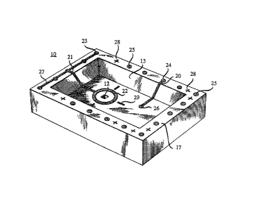
appropriate conductive features thereon. Exemplary features are shown in FIG. 2,15 wherein 22 is an annular conductor surrounding the opening in the well bottom,
27 is a linear conductor connecting bonding pads 23 on the second face, and 21 is
a linear conductor connecting 22 and 27. Bonding pad 24 on the second face is
connected by means of conductor 20 to bonding pad 25 on the bottom of the well.
Bonding pads 25 are (optional) spares tha~ are not joined to any conductive feature
20 in this exemplary embodiment, but that provide additional structural support and
thermal conduction paths when the assembly is mounted on a substrate. Fiducial
marks 28 and 29 are optional alignrnent features. The conductive featl~es are
forrned using a non-planar lithographic process that comprises vacuum-depositionof Ag2Se/GexSel x resist (see, for instance, E. Ong et al, SPIE Vol. 394, Optical
25 Microlitho~raphy II, pp. 39-48, 1983), selective exposure of the resist layer in a
standard contact printer, and development in a te~ramethylammonium
hydroxide/sodium sulfide bath.
Even though both FIGS. 1 and 2 show an individual body 10, it will
be appreciated that ihe processing up tO and including formation of the
3û metallization typically and advantageously is carned out on a wafer containing
hundreds or even thousands of potential bodies 10. Such a wafer is then diced bya known technique such that a multiplicity of processed bodies results
(exemplarily of approximate dimensions 2x2 mm), of which body 10 of FIG. 2 is
representa~ive. It will also be appreciated that the inven~on is not limited to an
35 assembly comprising one well ancl one aperture, but instead can be embodied in a
~3~2S5
- 7 -
variety of designs, including assemblies for coupling a muldplicity of fibers to a
multiplicity of opto-electronic devices and complising a multiplicity of through-
apertures and one or more wells.
FIG. 3 schematically shows body 10 in a view thae reveals features of
5 the first surface, namely, through-aperture 12, and optional grooves 30. The
grooves are advantageously produced by selective etching and will typically
enhance the adhesion to the first body of epoxy or other substance used to attach
an optical fiber to the body.
FIG. 4 schematically depicts a body 10, with opto-electronic device 40
10 (exemplarily a P~N diode) placed face down into the well such that the active cuea
of the device is over the opening in the well bottom, and the device is
conductively connected to the conductive means that extend from the second face
into the well. Exemplarily, an annular conductor on the front face (as depicted in
FIG. 4 this is the lower major surface) of the device 40 is conductively bonde~
15 (e.g., by means of solder or epoxy) to the corresponding feature on the bottom of
the well, and wire 41 is bonded, by a known technique, to the bonding pad (20 ofFIG. 2) and to a metallized region on the back face of the device.
FIG. S shows schematically and in cross sectiun a coupling assembly
according to the invention, with an opto-electronic device 40 conductively
20 attached to the conducdve features on first body 10 in the manner described
above, and with an optical fiber 52 maintained in a position adapted for opticalcommunication between the fiber and the opto-electronic device. The fiber is
shown to have a stripped back coating 53 and is attached to the first body by
adhesive means 51, e.g., epoxy. Other attachment means are known to the art and
25 can be used if desired.
A coupler according to the invention can be assembled in ~ny
convenient manner. For instance, the fiber can be inselted into the aperture andadhesively secured to ~he f~rst body, the opto-elec~onic device can be placed into
the well, be positioned coarsely and tempora~y elec~ical connec~ions established.
30 The device can then be energized and its position vaIied until maximum coupling
between fiber and device is attained, upon which the device is permanently
secured in the well. For instance, if the device is a detector then radiation of the
appropriate wavelength can be coupled into the fiber such that it is guided to the
coupling assembly and impinges upon the ac~ive region of ~he device. The
35 position is fine adjusted by maximizing the output of the detector.
~3~2S5~
In a currently preferred assembly procedure the opto-electronic device
is placed, by means of robotic equipment, into the well such that the active region
- of the device is centered upon the opening in the bottom of the well, and secured
to the first body such that electrical contact is established between the annular
5 conductor on the bottom of the well and the corresponding conductor on the front
face of the device. The presence of the above referred to opdonal fiducial markscan aid in the precise placement of the device, such that typically the desired
coupling efficiency (exemplarily < 2 db coupling loss) can be attained without
active alignment of the device.
After completion of the electrical connections to the device (e.g., by
wire bonding) and mounting of the assembly on an appropnate substrate an
appropriately prepared (e.g., cleaved and/or polished) stripped end of an optical
fiber is inserted into the aperture and secured to the first body such that the axis of
the secured end of the aperture is substantially parallel to the axis of the aperture.
15 Optionally, it is possible to introduce index matching mater~al between the end of
the fiber and the front face of the device.
Frequently it will be found desirable to provide strain relief means to
assure the physical integrity of the coupling assembly under the stresses normally
encountered. In particular, means for providing stram relief of the fiber wi~
20 respect to the first body are advantageously provided. Such means can be readily
devised by those skilled in the art, and a par~icular embodiment is schematically
depicted in FIG. 6, wherein numeral 10 refers to a coupling assembly according to
the invention (the opto-electronic device is not shown~, with a length of optical
fiber attached thereto. The coupling assembly is conductively mounted on an
25 appropriate substrate 60, exemplarily a Si subs~ate of the type described in
U. S. Patent 4,675,717, which is an example of an approach frequently referred to
as wafer-scale integration. Shown are also IC chips 64 and 65, representative of a
wide variety of chips that can be used in conjunction with the inventive coupling
means, which are also mounted conductively on the substrate, ç.g., by means of
30 solder attachment, as is schema~cally indicated in the drawing. Substrate 60 in
turn typically is mounted on a further substrate 61, exemplarily a multilayer
ceramic body comprising appropriate metallization. Electncal connections
between 60 and 61 are provided by conventional means, as is schematically
indicated by me~ms of wires 62, each bonded to a bonding pad each on 60 and on
35 61. Means are provided to make electrical contact with substrate 61, exemplarily
~3~255~
g
indicated by contact pins 63, arranged, for instance, such as to per nit plugging ~he
depicted assembly into an appropriate socket. Strain relief for the optical ffber is
provided by means of lid 66 and inset 67, the latter closely surrounding the
fiber 68. The lid typically is adhesively secured to the substrate, and the inset
S typically is similarly secured to the lid. The fiber optionally is secured to the
inset with epoxy or other appropriate means.
FIG. 7 schemadcally depicts an exemplary further embodiment of the
invention. Numeral 10 refers again to a first body, with opto-electronic device 40
mounted in the well, and 70 refers to a second body that advantageously also is
10 manufactured from single crystal Si. The second body comprises a through-
aperture adapted for accepdng therein an end of an optical fiber 52, and furthercomprises means that permit introduction of radiation focusing means between theend of the fiber and the opto-electronic device. Exemplarily the through-aperture
in the second body has the shape of two truncated pyramids 72 and 73 that meet
15 at their truncation planes, as indicated in FIG. 7, and the focusing means comprise
spherical lens 71 (e.g., a sapphire sphere) that is confined in the space provided by
the through-apertures. Desirably the inventive assembly is designed such that the
end of the opdcal fiber is in one focal plane of lens 71 and the active region of
the device 40 is in the other focal plane. The through-aperture of the second body
20 can readily be produced by lidlogr~phy and selective etching if the second body is
(100) oriented Si. It will be appreciated that the through-apertures need not bepyramid-shaped but could have other configurations, e.g., be substantially cone-shaped.
After placing the focusing means 71 into the space provided therefor,
25 typically the second body is secured to the first body, e.g., by means of an
adhesive layer at the inter~ace, or by clamping means (not shown) to form a
separable connector, and the fiber is secured tO the second body, e.g., by means of
a quantity of epoxy 51. If desired, posltional fine adjustment can be carried out to
further increase the coupling efficiency. Optionally index matching material can30 be placed into the space between the fiber and the lens and the lens and the
device. Electrical contact with the device is established substantially as discussed
above. Strain relief can be provided, e.g., substantiaily as shown in FIG: 6.
In both of the above discussed embodiments of the invention, the axis
of the attached optical fiber is substantially normal to the faces of the first bocly.
35 However, this is not necessarily the case, and FIC;. 8 schematically depicts an
- 10-
embodiment wherein the axis of the attached optical fiber is substantially parallel
to the faces of body 80. Groove 81 is optionally provided to receive the end of a
length of optical fiber, and is advantageously formed by means of
photolithography and selective etching, as is through-aperture 82, which
S advantageously is defined entirely by [111] facets. Body 80 further can comprise
a well (and associated conductive means, etc.) substantially as previously
described, or it can comprise a feature that permits accommodation of focusing
means, substantlally as described above in conjunction with FIG. 7. In either case
means are provided for reflecting a light beam such that a fiber rnounted such that
10 its end is substantially parallel with the faces of body 80 is optically coupled with
an opto-electronic device mounted in the well of a first body. Exemplary means
for accomplishing this purpose are also depicted in FI(:;. 8, wherein block 83 is
shaped to fit into through-aperture 82 as indicated. Face 84 of the block typically
is metallized such as to be a good reflector of radiation at the operating
15 wavelength of the coupling assembly, and is oriented so as to be substantially at
45 with respect to the fiber axis. Block 83 can be made from Si by selec~ive
etching and other known micromachining procedures, but it can also be made
from other materials (e.g., molded plasdcs). It will be appreciated that inventive
coupling assemblies with fibers entering parallel to the faces of the first bocly can
20 be mounted in substantially the same way as assemblies with peIpendicular fiber
entry, with obvious modifications of the strain relief means typically being
required.
Finally, it is to be understood that the above-described structures and
processing techniques are only illustrative of the principles of the present
25 invention. In accordance with these principles, numerous modifications and
alternatives may be devised by those skilled in the art without departing fiom the
spirit and scope of the invention. Thus, for example, although primary emphasis
herein has been directed to coupling assemblies made of silicon, it is apparent that
blocks made of other materials may also be lithographically patterned in the
30 unique way desc~ibed herein to form microrniniature coupling assemblies.