Note: Descriptions are shown in the official language in which they were submitted.
L3~2S9~
FULL COLOR LIQUID CRYSTAL DISPLAY
BACKGROUND
Field of the Invention
The present invention relates to fuIl color dis~
plays. More particularly, this invention pertains to an
improved liquid crystal display of the type that is
illuminated by both ambient and artificial light.
Description of the Prior Art
At present, full color displays for use in
aircraft and military vehicles commonly utilize a cathode
ray tube ~CRT). While such displays provide adequate
resolution and brightness, they are relatively bulky,
consume much power in operation and often require cooling
systems that further contribute to the bulk and the power
consumption of the total system. These factors are often
of critical importance to the design of airborne systems.
The drawbacks of full color CRT displays have led
to investigation of the feasibility of full color displays
based, inter alia, upon the use of a layer of electrooptic
liquid crystal material. Liquid crystal technology offers
the possibility of flat, relatively thin and therefore
o~s~g
highly compact construction. Further, the voltages and
power levels required to actuate liquid crystal materials
to a preferred orientation for modulating incident light
are relatively low.
The principal classifications of liquid crystal
material are twisted nematic, guest-host (or Heilmeier) ,
phase change guest-host and double layer guest-host. The
particular liquid crystal material employed dictates the
type of optical modulation that is effected by the light
valve. For example, twisted nematic material causes the
polarization of the light passing therethrough to become
reoriented (usually by ninety degrees). Guest-host
materials, so-called by the presence of a dye that aligns
itself with the liquid crystal molecules, modulate light
as a consequence of the property of the dye to absorb or
transmit light in response to the orientation of the
molecules of the li~uid crystal. In phase change guest-
host materials, the molecules of the liquid crystal
material are arranged into a spiral form that blocks the
majority of the light in the "off" state. The application
of a voltage aligns the molecules and permits the passage
of light. A double layer guest-host li~uid crystal
comprises two guest-host liquid crystal cells arranged
back-to-back with a ninet~ degree orientation between the
molecular alignment o~ the two cells.
~l3(~ 9 (
Liquid crystal displays may be arranged to operate
in a transmissive mode, a reflective mode, or both.
Generally, the reflective mode is most suitable for
operation under high ambient light conditions while the
transmissive mode, requiring backlighting, is most
usefully employe~ in applications involving dark and low
ambient (e.g. office) lighting conditions. The combina-
tion of both modes of operation is known as the "trans-
flective" mode of operation. This mode is particularly-
appropriate for broad range operation which includes, ofcourse, many important applications including, for
example, the en~ironment of the cockpit.
Presently, liquid crystal displays for operation
in the transflective mode comprise a liquid crystal light
valve in combination with a source of artificial visible
backlighting. A light diffusion plane is located inter-
mediate the light source(s) and the light valve. The
optical properties of the plane generally represent a
compromise between the needs to (1) transmit artificial
backlight and (2) reflect ambient light, when available,
through the liquid crystal light valve. The state of the
liquid crystal material is spatially controlled by a
transparent electrode matrix. ~When an active device such
as a thin film transistor or "TFT" is incorporated into
i'
" ~30Z5~
the array to enhance the addressability of the matrix, it
is known as an active matrix display.) Pixel locations
are addressed and the molecules of the adjacent liquid
crystal material are modulated so that a spatial distribu-
tion of pixel areas of preselected varied ligh~ transmis~sion is attained. In a full color display, a full color
filter that comprises a matrix or mosaic of individual
(narrow band) primary color ilters provides the sole
means for selecting the desired color band of the white
light ~transmitted backlighting and reflected ambient
light) that passes through the liquid crystal material
layer. ~ight absorbing dyes form the (red, green and
blue) col'or elements of the matrix. The color elements of
the filter are in registration with the elements o the
electrode matrix so that, by addressing the electrodes in
accordance with the color coding of the filter matrix, the
transmission o~ white light ~hrough the liquid crystal
material produces a full color display. A representative
display of this type is disclosed in United States pa~ent
Serial No. 3,840,695 of Fischer for "Liquid Crystal Image
Display Panel With Integrated Addressing Circuitry."
Displays in accordance with the above-described
typical arrangement are beset with many difficulties. The
use of absorbing dye filters to color the image passing
through the li~uid crystal layer represents a highly
. ~ 13~S~
-
inefficient usage of the energy contained in the light
source. Each dedicated filter element essentially blocks
the transmission of two thirds of the white liyht through
the valve. That is, in the prior art, each pixel is
illuminated with white light, requiring that color filters
transmit only the desired portion of the white light
spectrum while absorbing all other wavelengths. In total,
~ about one third of the energy from the white light source
is transmitted through each of the filter "windows".
This energy absorption effect is even more
dramatic with respec~ to the utili~ation of (reflected)
ambient light by the display. Reflected light must pass
through the filter twice, multiplying the energy loss. As
a result, the display is often unsuitably dim. Correction
for such dimness often involves an increase in the power
level of the backlighting that, in turn, introduces
additional undesirable effects~ In addition to
conflicting with the goal of a low energy display, this
may produce harmful temperature rises within the system.
The design of a single filter for coloring both
backlight and ambient illumination is further complicated
by the different chromaticity effects experienced by the
reflected light which passes twice through the filter and
the transmitted light that passes only once through that
Z59~ ~
filter. This disparity can result in a display of
differing hues during high and low ambient lighting
conditions.
Another deficiency of the conventional approach is
that, in the desire to minimize undesirable parallax
effects, the color filter elements must be closely located
immediately adjacent the li~uid crystal layer. Thus, the
diffusion (or back) plane, which must be behind the liquid
crystal layer, is recessed by the thickness of the glass
layer at the rear of the liquid crystal. The resultant
spacing of the filter and the somewhat-reflective back-
plane can produce two deleterious effects during reflec-
tive mode operation o~ the display. Ambient light will
generally include off-axis rays. When ambient light is
absorbed in the liquid crystal layer, it creates a shadow
on the diffusing plane along the axis of the incident
light. Therefore, as the display is viewed at an angle
with respect the direction of such incident light, the
image appears to be displaced with respect to the image
created in the liquid crystal layer. This results in an
annoying double image or "shadowing" effect. Of perhaps
even greater significance, the spacing of the backplane
from the color matrix can produce cross-contamination
between the primary colors of the filter. This results
when an oblique, off-axis ray of ambient light passes
~3025~
through a filter of one primary color when incident upon the
front of the light valve and then exits the valve through a
filter of a second primary color after reflection from the
backplane.
S~qMARY
The present invention overcomes the above-referenced
shortcomings of the prior art by providing a novel display.
In a first aspect, the display of the invention includes a
plurality of adjacent light-conducting cells disposed in a
planar array, each cell having means associated with it for
modulating the amount of visible light passing therethrough.
A phosphor layer is provided beAind the cell array, the layer
being capable of emitting visible light through the array
when irradiated from behind with ultraviolet light. An
ultraviolet light source is provided behind the phosphor
layer for irradiating the phosphor layer with ultraviolet
light; and a fiber optic plate is disposed behind the cell
array and in front of the phosphor layer. The plate includes
a plurality of adjacent and parallel light-conducting pipes,
each pipe comprising a bundle of optical ~ibers and having a
front end in light-conducting communication with one of the
cells, and a rear end in light-conducting communication with
the phosphor layer.
In a further aspect, there is provided a combination
that includes a light-conducting plate having front and rear
faces and a plurality of adjacent and parallel optical-fiber
light pipes extending between the faces, each pipe comprising
a bundle of optical fibers. A filter layer is formed
directly on the rear face of the plate. A matrix of distinct
phosphor element is deposited directly on the filter layer,
each element being in registration with a rear end of one of
the light pipes and capable of emitting visible light
rn/
~L3~2~9~
therethrough when illuminated by fluorescent light. An array
of distinct transparent control electrodes is deposited
directly on the front face of the plate, each electrode being
in aligned registration with one of the phosphor elements
through a front end of one of the pipes. A source o*
fluorescent light is positioned behind the plate for
illuminating each phosphor element with fluorescent light;
and a layer of liquid crystal material is positioned adjacent
to the electrodes on the front face of the plate, the layer
and the electrodes having means associated therewith for
defining an array of li~ht-conducting cells in registration
with the pipes and for modulating the amount of light passing
through corresponding ones of the cells and the pipes.
The preceding and other advantages and features of
this invention will become further apparent from the detailed
description that follows. This wrikten description is
accompanied by a set of drawing figures that include numerals
thereon corresponding to reference numerals of the
description. Such numerals point out the various features of
the invention, like numerals referring to like features of
the invention throughout.
BRIEF D~SCRIPTION OF THE DRAWINGS
Figure 1 is an exploded perspective view of the
arrangement of a light valve for use in a full color display
in accordance with the invention; and
Figure 2 is a schematic side view of a full color
liquid crystal display in accordance with this invention that
serves to illustrate its operation.
DESCRIPTION
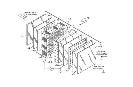
Turning now to the drawings, Figure 1 is an exploded
perspective view of a light valve 10 for use in a full color
liquid crystal display in accordance with this
rn/
- ~ ~L3~259~ (
invention. Some of the details o~ construction of the
light valvè 10 have been omitted for purposes of clarity
from the representation of Figure 1. However, it will be
appreciated by those skilled in the ar~ that such omitted
details relate to matters that are well known in the art.
The description of the structure of the light
valve of Figure 1 will proceed from its rear or backside
which accepts the output from one or more sources of
ultraviolet radiation to the front surface through which
ambient illumination enters the cell. A plate 12 forms
the rear surface of the light valve 10. The plate 12,
preferably quartz, transmits ultraviolet radiation. A
first dichroic selective filter layer 14 is deposited on
the inner surface of the plate 12. The dichroic filter 14
is fabricated of material that is transmissive to
ultraviolet radiation and reflects visible light. The
significance of such arrangement will become further
apparent from the discussion of the invention that
; accompanies Figure 20
A unique fiber optic plate structure 16 is located
adjacent the filter layer 14 of the plate 12. This
structure 16 includes a fiber optic plate 18 of about .05
inches in thickness having distinct structures, in
registration, at its opposed surfaces. At the rear or
. 9
. :
. -
~3~;gg
backside of the plate 18, is a second dichroic filter 19.The dichroic filter 19, shown and discussed further in
conjunction with Figure 2, differs from the first dichroic
filter 14 in that it is fabricated of material that
reflects ultraviolet and transmits visible radiation. A
phosphor layer 20 is deposited onto the surface of the
filtPr 19. The layer 20 may comprise a matrix arrangement
of a plurality of discrete phosphor elements. (The term
"phosphor", as used herein, includes any material that
iO converts energy from an external excitation and, by means
of the phenomenon of phosphorescence or fluorescence,
converts such energy into visible light.)
In SUC}l a matrix, each phosphor element is aligned
in registration with a corresponding elements of the
electrode pattern 23. The matrix may contain a single
type (i.e. wavelength emission spectrum) of phosphor or a
plurality of phosphor types for providing a multi-color
display. In the case of a full color display, a plurality
of phosphors, each of which emits one of the primary
colors upon excitation by ultraviolet radiation, is
preferably arranged into a recognized format. This may
include, for example, the conventional triad, quad (in
which the green component is doubled) or fixed format
geometries. The phosphors may be deposited by any of a
number of well known processes including settling, screen
~3~2~
printing and photolithography. These processes are also
commonly employed in the fabrication of CRT screens.
As an additional fèature, each of the plurality of
phosphors 20 may be colored (body color) such that the
chromaticity of the reflectance spectrum closely matches
that of the phosphor's emission spectrum. The purpose of
such pigmentation is to prevent the "washing out" or other
introduction of color impurity into the image emitted by
the excited phosphors. This can occur in the presence o~
high ambient illumination by the superposition o~ the
color reflected from the surfaces of the phosphors.
An active electrode matrix 22 comprising metal-
lized buses and transparent electrodes 23 is formed on the
front of the fiber optic plate 18. The arrangement and
fabrication of such an electrode matrlx for spatially
distributing a plurality of liquid crystal level voltages
is ~lell known in the art and is disclosed, for example, in
the Fischer patent referenced above. Generally, such a
structure may be formed by vacuum deposition of metallized
electrodes. ~ielectric inter-layers are provided for
necessary insulation. The electrode matrix 22 is prefer-
ably an "active" matrix that associates a semiconductor
device (transistor or diode) with each node of the bus
structure. Such active electrode-arrays facilitate the
-
599
addressing of large element arrays.
The phosphor and active electrode matrices are
aligned by well known techniques. By forming both of
these critical devices onto a common material, the reg-
istration of corresponding elements of the -two matrices is
maintained and is not affected by differential temperature
expansions. The fiber optic plate 18 may comprise two
independent plate elements to facilitate the two quite
different (electrode and phsophor matrix) fabrication
processes necessarily undertaken with respect to its front
and rear faces.
A layer of liquid crystal material 24 is po-
sitioned adjacent the front surface of the fiber optic
structure 16 in intimate contact with the active electrode
matrix 22 formed at the front surface of the plate 18.
This layer is preferably formed of guest-host (Heilmeier)
liquid crystal material as this material is known to have
a good gray-level characteristic (i.e. linearity of the~
voltage-light transmission relationship). However, phase
change guest-host material is equally compatible with the
geometry of the invention. The general arrangement of the
invention is further compatible with the additional
structural layers required to accommodate double layer
guest host liquid crystal material.
12
~3~2~;~9
A layer 26 of transparent conductive material such
as ITO (indium tin oxide) is located at the front surface
of the liquid crystal 24 and is generally maintained at a
reference potential with respect to the address and data
voltages applied to the active matrix. The layer 26 acts
as an equipotential surface that provides the common or
counterelectrode of the display.
The layer 26 coats the interior surface of the
color filter 30. The front plate 28 admits ambient light
into the light valve 10 from the environment and transmits
the visible light emitted by the phosphors 20 and
reflected from surfaces of the phosphors and the first
filter 14 and then transmitted through the liquid crystal
layer 24. The plate 28 is preferably fabricated of
glass having a coefficient of thermal expansion which
closely matches that of the fiber optic plate 18. Such
matching of coefficients minimizes stressing of the
required hermetic seal (not illustrated) between the
window layer 28 and the fiber optic plate 18. Such a
hermetic seal prevents both leakage and contamination of
the liquid crystal material 24.
A color filter 30 may be optionally deposited onto
the front plate 28. The filter 30, comprising a matrix of
., ~ .
L3~2Sgg
light absorbing dyes (each in registration with a like-
colored phosphor of the matrix 20), provides an alter
native to body coloxing the phosphors to prevent the image
washout at high ambient illumination that could otherwise
S occur. While the arrangement of dye elements of the
filter 30 and its principle of operation are the same as
that o~ a color filter of the type that is commonly
employed on prior art li~uid crystal displays, the filter
is qualitatively different in both structure and
operation in that its individual filter elements are not
as wavelength selective as those of the filters of prior
art full color displays. This is a result of the fact
that, in the liquid crystal displa~ system of the
invention, the filter 30 is not the sole available means
for coloring the output image. Rather, as will be seen
from the discussion that accompanies Figure 2, the primary
sources of colored light for the display are the visible
colored light emissions of the excited phosphors 20.
The visible llght emissions of colored light from
the phosphors generally have a narrow bandwidth and
exhibit well saturated chromaticity that is similar in
performance to the outputs fxom the cathode luminescent
phosphors used in color CRT's. The outputs from the
phosphors are necessarily superimposed upon the color
filter elements that are illuminated by reflected ambient
~.3~)25~
light. Thus, the filter 30 needn't have the same selec-
tivity as the light absorbing filters of prior art liquid
crystal displays that rely solel~ upon a dye filter to
color the ouput image. As a result, the design of the
filter 30, as opposed to filters for prior art liquid
crystal displays, is of a lesser wavelength selectivity,
features a much wider passband, and may be employed with a
correspondingly reduced effect in terms of its absorption
of the energy input ~both natural and artificial) to the
display. A much higher percentage of white light is
transmitted through the absorbing filter 30 of the display
of the invention than is transmitted through the type of
filter that is commonly employed in prior art liquid
crystal displays. The effect of the increased trans-
missivity of the filter 30 becomes even more pronounced inthe reflective mode as reflected ambient light passes
through the filter 30 twice (upon both incidence and
reflection~.
The final element of the light valve 10 is an
optional polarizer 32. This polarizer is re~uired for
operation of the display when a guest-host (Heilmeier)
type material is employed for the liquid crystal layer 24
but would be unnecessary in a display that utilizes a
phase change guest-host material. This reflects the
differing modes of physical operation of these two types
C ~30;~:5~ ~
o~ liquid crystal materials.
Figure 2 is a partial side view of a liquid
crystal display arrangement in accordance with the
invention. Certain elements of the light valve 10 of
Figure 1 have been omitted and others are shown somewhat
schematically in this figure to assist in the accompanying
discussion.
A fluorescent lamp 34 is positioned at the
backplane of the light valve 10. The electrodes of the
lamp 34 are enclosed within a clear envelope of quartz or
other ultraviolet-transmissive material. Thusj the output
of the lamp 34 comprises ultraviolet radiation 36 rather
than visible light. As will become apparent from the
discussion that follows, the output of the lamp 34 is
chosen for its ability to excite the phosphor matrix 20 to
emit visible light. In general, the dominant emission
spectrum of the lamp 34 is between 254 nm and 365 nm.
This spectrum is, of course, selected so as to match the
excitation spectrum of the phosphors. Other energy
sources, including electron beams are known to excite
phosphors to emit visible light and may be substituted for
the fluorescent lamp 34.
The invention utilizes the intrinsically high
16
.
~3025~9
energy conversion efficiency (visihle light emitted per
unit of energy applied) of flourescent illumination.
Whereas an incandescent lamp exhibits an overall ef-
ficiency of approximately 15 lumens per watt, the ef-
ficiency of flourescent illumination exceeds S0 lumens per
watt. Unlike prior art systems that have sometimes
utilized flourescent lamps as a source of visible white
light that is thereafter colored by means of lossy
filters, the present invention obtains the maximum
available energy efficienc~ offered b~ the utilization of
flourescent energy.
The ultraviolet radiation 36 from the lamp 34 is
t;ransmitted through the first dichroic filter 14 prior to
reaching the phosphor matri.Y 20. As the radiation 36
reaches the phosphors of the matrix 20, the ultraviolet
radiation is, in turn, converted to colored visible light
at a relatively high efficiency (in excess of eighty per
cent). This is to be contrasted to the prior art wherein
the generation of colored light is quite inefficient due
to the high absorption of the visible white light by a
narrowband dye filter. In such a prior art system, about
thirty per cent of the incident energy is transmitted.
The actual amount of transmission achieved is dependent
upon the bandwidth of the filter. Well saturated, or
narrow bandwidth, colors can only be realized at the
~. .
- ~ ~3~)2~ 9
expense of increased selectivity and consequent additional
energy loss.
The ultraviolet radiation 36 that is not initially
absorbed by the phosphors 20 is reflected from the second
filter 19 and may thereafter be absorbed by the phosphors,
further increasing the efficiency of the system.
The visible colored light 40 emitted by the
phosphors is radiated toward both the front and the back
of the light valve 10. Due to the visible light reflect-
ivity of the dichroic filter 14, the phosphor emissionsthat travel toward the backside of the light valve 10 are
reflected therefrom and toward the front of the display.
The close spacing between the phosphor matrix 20 and the
adjacent dichroic filter 14 allows only minimal "spread-
ing" of the reflected phsophor outputs. Thus, a highpercentage of this reflected light is available for
illumination of the display after travelling through the
light "pipes" of the fiber optic plate 18 and the trans-
missive portions of the liquid crystal layer 24.
The dichroic filter 14 additionally reflects the
incoming ambient light. The portion of ambient light
reaching the filter 14 represents the residue of the
incoming light that is incident upon the diffusing
18
..
.~ .
:: .
. .
.
,: ,
: , .
~3~2599
surfaces of the phosphors 20. As mentioned earlier, the
eff~ct o~ that light insofar as reducing the purity of the
backlit image produced by the display is corrected by
either the coloring of the phosphor bodies to match their
emission spectra or the additlon of the optional dilute
color filter matrix 30 at the front of the light valve 10.
The ambient light 42 enters the valve 10 through
the front plate 28, polarizer 32 (in the event that a
Heilmeier liquid crystal material is utilized) and
(optionally), the dilute filter 30. (These elements of the
light valve are not shown in Figure 2.) After passing
through the transparent counterelectrode 26 and the light-
modulating layer of liquid crystal material 24, it reaches
the fiber optic plate 18. As mentioned earlier, the
active electrode matrix 22 comprising a conventional array
of busses and transparent drive electrodes 23, in regis-
tration with the phosphor matrix at the back of the plate
18, is located on the front surface of the plate 18.
As can be seen from Figure 2, the opticaI fibers of
the plate 18 can be thought of as grouped into a plurality
of "pipes" 38 for transmitting light therethrough. Each
pipe 38 underlies a single phsophor 20lof the matrix and,
due to the registration of the phosphor and electrode
matrices, transfers light toward the associated
19
.. ~ . .. ,. ;; .. ,~ .
~ ( ~31~2~9
transparent electrode 23 on the opposed face of the fiber
optic plate 18. Each of the phosphors of the matrix 20
corresponds to a single pixel of the display, each pixel
being about .010 inches square. Between 50 and 100
optical fibers of the plate 18 comprise an individual
light pipe 36 for transferring the full color illumination
of the phosphor matrix 20 to the front surface of the
plate 18, adjacent the layer of li~uid crystal material
24. The individual phosphor dimensions match those of the
electrode matrix and a typical display panel will include
approximately 250,000 to 1,000,000 phosphor elements or
pixels. Visible light that is incident at either surface
of the plate 18 will be transmitted through a pipe 38
comprising a plurality of adjacent optical fibers. The
image is dissected by the individual optical fibers o~ the
plate 18 and the total image is transferred through the
individual optical fibers without significant dispersion.
Thus, the plate acts as a relay lens, transferring the
image plane of the phosphors to close proximity to the
liquid crystal layer.
In the event that the phosphors of the matrix 20
are not colored and the optional filter matrix 30 is
utilized, the above-described process whereby off-axis
incident illumination is screened by the fiber optic plate
18 similarly prevents cross-contamination of the colors of
. ~ ... ,, ., ,,~ ~ .. .
. ...... :
- ~3~12~i99
the display and assures tha-t the ambient illumination will
enhance the color quality of the image. As mentioned
above, the colored windows of the filter 30 are aligned
with the matching color-emittlng phosphors of the matrix
20. By locating the fiber optic plate 18 intermediate the
filter 30 and the phosphors 20, the ambient light that is
incident upon the phosphors is required to travel and exit
through the particular color filter that is in
registration with the phosphor of the identical light
emitting color. The particular light path for a given
phosphor-filter combination is, of course shuttered (for
off, on and gray-level light transmission) by the
alignment of the molecules of the liquid crystal layer
24. Thus, ambient light is reflected only off the
phosphors that have been shuttered on the liquid crystal
layer 24.
Thus it is seen that there has been provided a new
liquid crystal display of the type that is illuminated by
both ambient and artificial light energy. As such, the
display is operable in the transflective mode. Although
reference has been made to liquid crystal light valve
material, it should be understood that other known types
of light valves or modulators may be adapted to the
present invention. Examples of such alternatives include
suspensions of polarizing particles in a host of liquid,
~L30~5~ ~
magneto-optical light modulators that utilize the Faraday
effect and piezoelectric light modulators.
- By utilizing a display in accordance with the
teachings of the invention, one can realize much higher
efficiencies in the utilization of input energy. This
beneficial result derives, in part, from a combination of
the generally low power requirements for modulating liquid
crystal material (as opposed to CRT technology) coupled
with a design that features the efficient energy trans-
formations that are inherent in the use of ultravioletradiation to excite phosphorescent matexial to narrow band
emissions of visible light.
While this invention has been described with
respect to its presently preferred embodiment, its scope
is not so limited. Rather, the scope of this invention is
only limited insofar as defined in the following set of
claims and includes all equivalents thereof.
, ,
" ' '