Note: Descriptions are shown in the official language in which they were submitted.
~;~0;~178
1 51,930
MULTIPURPOSE DIGITAL INTEGRATED CIRCUIT FOR
COMMUNICATION AND CONTROL NETWORK
CRQSS REFERENCE TO RELATED APPLICATIONS
The invention disclosed herein relates to two-
way communication and control systems. Canadian patent
application number 484,817 filed June 21, 1985, entitled
"Digital Massage Format for Two-Way Communication and
Control Network", inventors Leonard C. Vercellotti,
William R. Vérbanets Jr. and Theodore H. York, relates
to such communication and control systems.
This applicat10n is a divisional of Canadian
patent appllcation serial number 484,8t6 entitled
"MULTIPURPOSE DIGITAL INTEGRATED CIRCUIT FOR
COMMUNICATION AND CONTROL NETWORK." Other divisionals of
that application, and bearing the same title, are
Canadian patent applications:
serial numbers 594,777; 594,778; 594,779; 594,947;
594,948; and 594,949.
BACKGROUND OF THE INVENTION
A. Field of the Invention
The present invention relate~ generally to
information communication networks and, more
particularly, to communication networks by means of which
a large number of remotely posit;oned controllable
devices, such as circuit breakers, motor overload relays,
lighting systems, and the like, may be controlled from a
central or master controller over a common network line
~k
1303~78
2 51,930
which may comprise either the existing AC power lines, or
a ded;cated twisted pair line, or in some instances a
fiber opt;c cable.
The ;nvention particularly relates to a low
cost, multipurpose dig;tal integrated circuit (IC) which
can be used as the bas;c building block in establishin~
a network communication system over a desired
commun;cation l;nk. The d;gital IC can function as an
addressable microcomputer interface between the network
line and a remotely located microcomputer which may, for
example, comprise any microprocessor based controlled
product. In such mode, the d;gital IC's function is to
take data from the network and pass it on to the remotely
located microcomputer upon command from the central
controller and to transmit data from the microcomputer to
the central controll0r. The digital IC may also function
as a nonaddressable microcomputer interface between the
central or master controller and the network line. In
such case the digital IC's function is to continuously
take data from the central controller and place it on the
network and take data from th~ network and pass it back
to the central controller. The digital IC may also
funct;on as an addressable load controller associated
with an individual remote controlled dev~ce and
responding to shed or restore load commands from the
central controller over the network line. When so used
the digital IC may also be commanded to transm;t a reply
message back to the central controller giving informat;on
as to the status of the controlled dEv;ce, thus enabl;ng
~0 the central controller to mon;tor a large number o~
remotely located controllable devices.
B. DescriPt;on of the Pr;or Art
Various commun;cat;on and control systems have
been heretofore proposed for controlling a group
1303178
3 51930
of remotely located devices from d central controller over
a common network line. Control systems for controlling
distributed electrical loads are shown, for example, in
Miller et al U.S. Patent Nos. 4,167,786, 4,367,414 and
4,396,844 issued September 11, 1979, January 4, 1983 and
August 2, 1983, respectively. In such systems a large number
of relatively complex and expensive transceiver-decoder
stations, each of which includes a microprocessor, are inter-
connected with a central controller over a common party line
consisting of a dedicated twisted pair for bidirectional
communication between the central controller and all trans-
ceivers. Each of the transceiver-decoder stations is also
of relatively large physical size due to the fact that a
substantial amount of hardware is required, in addition to
the microprocessor, to receive and transmit signals. Also,
both the hardware and microprocessor consume substantial
amounts of power. In fact, in Miller et al U.S. Patent No.
4,167,786 it is necessary to provide a powersaver mode in
which the major portion of the circuitry at each remote station
is denergized to reduce power consumption during intervals
when load changes are not being actuated.
Each of the transceiver-decoder stations controls
a number of loads which must be individually connected to a
particular transceiver by hardwiring, these interconnections
being quite lengthy in many instances. In such a system, all
transceivers can initiate messages at any arbitrary time in
response to control input from the associated switches. Ac-
cordingly, it is not uncommon for two or more transceivers
to simultaneously sense a free common party line and begin
simultaneous transmission. This requires a special bus
arbitration scheme to cause all but one of the interfering
transceivers to drop out of operation while permitting
one selected trans-
1~03~78
4 51~3~
ceiver to continue its data transmission. Al~o, in
such a ~ystem transmission from the tran~ceiver to
the central controller is very limited and consists
merely of an indication of a manually opera~le or
condition responsive switch or analog sen~ors such as
a thermistor or other analog sensing device. In the
load distribution control system shown in the above
referenced prior art patents, the arbitration tech-
nique is dependent on the impedance levels of the
active and inactive states of the data line. If the
data line ~ecomes stuc~ in a low impedance state, due
to the failure of one of the connected transceiver
decoders, further communication over the network line
is prevented until the malfunctioning transceiver is
pnysically disconnected from the data line.
In the communication and control system de-
scribed in tAe above identified Miller et al patents
a message transmitted over the network include~ a
preamble portion of a minimum of four bits. Tnese
preamble bits comprise 50% square waves which are
utilized by the transceiver decoders to permit a
phase lock loop circuit in each transceiver to lock
onto the received pream~le bitS. The use of a mini-
mum of four bits to provide phase loop lockon reduc~
~9 the overall throughput of such a system. Also,
in order to capture the preamble bits it is necessary
to provide the phase loc~ loop circuit initially with
a relatively wide bandwidth of a~out 5KHz and then
narrow down the bandwidth after the phase 10CK loop
circuit has locked onto the pream~le ~its. Such an
arrangement requires additional circuitry to accom-
plish the necessary change in bandwidth. Also, the
relatively wide ~andwidth necessary to capture the
preamble bits also lets in more noise so that the
security and reliability of the system is reduced in
noisy environments.
1303178
51~30
SUMM~RY OF THE INVENTION
In the presently described commun$cation
network a small low cost digital I~ lS employea which
can be readily adapted by merely grounding different
input terminal~ of the IC to perform all of the dif-
ferent functions necessary to the component parts of
the complete communications network. Thus, in one
pin configuration of the digital IC it can function
as an addressable load controller, responding to shed
or restore load commands from the central controller
and replying back to the central controller with
status information regarding the state of the con-
trolled load. This mode of functioning of the digi-
tal IC is referred to as a stand alone slave mode of
operation. In the stand alone slave mode the digital
IC is arranged to ~e directly associated with each
control device i.e. circuit breaker, motor control-
ler, lighting control, etc. and may, if desired, com-
municate with the master controller over the same
wires which are used to supply power to the control-
led device. This substantially reduces the amount of
wiring required to connect a number of controlled de-
vices to the common communication networ~. The cen-
tral controller may also issue ~lock shed and ~loc~
restore commands to a group of stand alone slaves to
which command they will all simultaneously respond.
Al~o, the central controller may issue a "scram" com-
mand to shed load which causes all stand alone slaves
(wbich may num~er as high as 4,0Y5) to simultaneously
shed their respective loads.
In another pin configuration of the digital
IC it can function as an addressable microcomputer
interface. In this so called expanded slave mode of
operation the digital IC provides an interface ~e-
tween the communication network line and a remotemicrocomputer which may, for example, wish to trans-
1;~03~78
6 SlY30
mit data over the communications network to the cen-
tral controller. In the expanded slave mode of the
digital IC the micro computer interface is disabled
until the central controller enables it ~y sending an
enable interface command addressed to the expanded
slave. After the microcomputer interface is enaDled
the central controller and the remote microcomputer
can communicate back and forth through the expanded
slave digital IC.
The digital IC may also be pin configured
to function as a nonaddressable microcomputer inter-
face, such functioning being referred to as the ex-
panded master mode of functioning of the diqital IC.
In the expanded master mode the interface with an as-
sociated microcomputer is always enabled and any net-
wor~ transmissions that the digital IC receives may
be read by the interfaced microcomputer. Also, the
interfaced microcomputer may transmit data onto the
network a~ any time through the expanaed master type
of digital IC. Accordingly, when the digital IC is
operated in this mode the interfaced microcomputer
may comprise the central controller of ~he communica-
tions netwoek.
The digital IC which may be adapted to per-
form all of the a~ove descri~ed functions, is also
arranged so that it can ~e used with different types
of data lines. Thus, in one pin configuration of the
digital IC it is adapted to transmit messages to and
receive messages from a networ~ line consisting of
3U tne conventional AC power line of a factory, office
building or home. Because of the significant phase
disturbances associated with such power lines, data
is transmitted over the networ~ by means of on-off
keying of a high frequency carrier. Preferably this
high frequency carrier has a frequency of 115.2 kHz
and the digital IC is arranged to transmit data at
130;~178
7 51~30
the rate of 300 bits per second ~300 baud) over con-
ventional power lines. The choice of a 115.2 kHz
carrier is based on empirical results of spectrum
analyses of typical power lines and tne 300 baud bit
rate is based upon desired system performance and ac-
ceptable error rates.
In tne presently described communication
system, the digital IC has a crystal controlled os-
cillator operating at a frequency many times higher
than the carrier frequency. The carrier signal is
derived from this crystal osciallator. The cry~tal
oscillator is also used as a source of timing signaLs
within each digital IC to esta~lish predetermined
baud rates for the transmission of data over the net-
work. Accordingly, the frequency of the carrier sig-
nal employed to transmit messages over the networ~
can be readily changed to avoid an undesired inter-
fering frequency by simply changing the crystals in
the crystal oscillator associated with each digital
IC. Such a change in carrier frequency will also
change the baud rates at which the communication
system operates, as described in more detailhereinafter.
The frequency of the crystal oscillator in
each digital IC is highly sta~ilized so that the car-
riec frequencies developed by the digital IC's at thecentral controller and remote stations are very close
to the same frequency although a received carrier
signal may drift in phase relative to the timing sig-
nals~produced in the digital IC which is receiving a
message. As a result, it is not necessary to trans-
mit a number of pream~le bits and provide a phase
lock loop circuit which locks onto ~he received mes-
sage durins the preamble bits, as in the above de-
scri~ed Miller et al patents. In the presently
de~cri~ed communication and control system the indivi-
dual digital IC's operate asynchronously but at su~-
1~03178
8 51Y30
stantially the same frequency so that any drift in
phase does not interfere with detection of the re-
ceived carrier signal, even at relatively low baud
rates and noisy environments.
In order to provide further noise immunity
when using noisy power lines as the common network
data line, the digital IC is arranged to compute a 5
bit BCH error code and transmit it with each message
transmitted to the network. Also, eacb message re-
ceived from the ne~work by the digital IC includes a
five bit BCH error code section and the digital IC
computes a ~CH error code ~ased on the other digit~
of the received message and compares it with the BCH
error code portion of the received message.
In order to provide still further noise
immunity when operating over conventional power
lines, the digital IC includes a digital demodulator
which has high noise rejection so that it can detect
on-off carrier modulation on power lines which have a
relatively high noise level. Empirical results show
that the digital demodulator portion of the digital
IC can receive messages with a ~it ~rror rate of le~s
than l in 100,000 for power line signal to noise
ratios of approximately 6 d~ at a 300 Hz ~andwidth.
Also, such digital demodulator can receive error free
33 bit messages at a 90% success rate in a power line
noise environment of only 4 db signal to noise ratio.
~hen it is desired to use a dedicated
twisted pair line as the common data line for tne
communication network, which usually has a lower
noise level than power lines, the digital IC is adap-
ted to transmit data to and from such twisted pair
line at 4 times the data rate mentioned above i.e. at
1200 bits per secona (1200 baud). Such adaptation of
the digital IC can be readily accomplished by simply
grounding a different one of the input terminals of
the digital IC.
i~O3~78
9 51930
The digital IC may also be pin con~igured
to accompllsh all of the above descri~ed functions in
a high speed communication network in which the com-
mon data line is a fiber optic cable. In this mode
of operation o the digital IC the digital demodulat-
or portion is bypassed and the remaining logic is
adapted to receive and transmit data messages at the
extremely high rate of 38,400 bits per second (38.4 k
baud~. In such a fiber optic cable communication
system the data is transmitted as base band data
without modulation on a hiqher frequency carrier.
The digital IC is arranged to transmit and
receive messages over the common networ~ in a speci-
fic message format or protocol which permit~ the es-
tablishment of the above described microcomputer in-
terface so that different microcomputers can communi-
cate over the common network while providing maximum
security against noise and the improper addressing of
individual digital IC's by the master controller.
Specifically, the message forma~ consists of a series
of 33 bits, the first two ~its of which comprise
start bits having a logic value of "l". The start
bits are followed by a control ~it which has a logic
value ~l~ when the succeeding 24 message ~its signify
the address of ehe digital IC and instructions to be
performed by the digital IC. When the control bit
has a logic value of "0" the next 24 message bits
contain data intended for the interfaced microcom-
puter when the digital IC is operated in an expanded
mode. The next ive message bits contain a BCH error
chec~ing code and the laqt message bit is a stop ~it
which always has a logic value o~ ~0".
When a 33 bit message is received ~y the
digital IC the first 27 bits thereof are supplied to
a BCH code computer portion of the ~igital IC which
computes a 5 bit BCH error code based on the fir~t 27
~30~3~7~
51930
bits of the received message. The computed BCH code
i~ then compared with the succeeding S bit BCH error
checking code of the received mesaage, on a ~it by
bit basis, to ensure that the received message has
been received and decoded properly.
In a similar manner when data is to be
transmitted onto the network either as a reply mes-
sage in the stand alone slaYe mode, or from the in-
terfaced microcomputer to the network through the di-
gital IC, the 8CH computer portion of the digital ICcomputes a 5 bit error checking code based on the
data to be transmitted and adds the computed 8CH
error checking code at the end of the stored data
bits as the 33 bit message is ~eing formatted and
transmitted out o~ the digital IC to the communica-
tion network. By thus employing BCH error code com-
puter logic in the digital IC for both receivea and
transmitted messages, the assurance of transmitting
valid, error free 33 bit messages in both directions
on the networ~ is greatly increased.
The digital IC which accomplishes all of
these functions is of small size, is readily manufac-
tured at low cost on a mass production basis and con-
sumes very little power. Accordingly, the overall
cost of the communication and control system is much
less than that of the above described prior art
patents while providing all of the addititional fea-
tures discussed above. Of particular importance is
the feature of providing a low cost interface to
microprocessors associated with controlled devices,
such as circuit breakers, motor starters, protective
relays and remote load controllers, so that tnese
microprocesSors~ which are busy with other tasks, can
be selectively interruptea and two-way communication
established between the central controller and the
selected microproCessor at a remote ~tation.
~303~78
ll 51930
BRIEF DESCRIPTION OF THE DRAWINGS
The invention, both as to its organization
and method of operation, together with further
object3 and advantages thereof, will best be under-
stood by reference to the following specificationtaken in connection with the accompanying drawings in
which:
Fig. 1 is an overall bloc~ diagram of the
described communication system;
Fig. 2 is a diagram of the message bit for-
mat employed in the system of Fig. 1 for a mes~age
transmitted from the central controller to 2 remote
station;
Fig. 3 shows the coding of the instruction
bits in the message of Fig. 2;
Fig. 4 is a ~essage ~it format for a reply
message transmi~ted back to the central controller
from a remote station;
Fig. 5 is a message bit format of a message
transmitted from the central controller to an inter-
faced microcomputer;
Fig. 6 is a diagram of the pin configura-
tion of the digital IC used in the disclosed system;
Fig. 7 is a bloc~ diagram illustrating the
use of the digital IC with a power line at 300 baud
rate;
Fig. 8 is a block diagræm showing the use
of the dlgital IC with a twisted pair line at 1200
Daud rate;
Fig. 9 is a D}OC~ diagram of the digital IC
uQed with a fiber optic ca~le transmission system at
38.4k baud rate;
Fig. 10 is a block diagram showing the use
of the digital IC in a stand alone slave mode;
Fig. ll is a block diagræm showing a modi-
fication of the system of Fig. 10 in which vacia~le
time out is provided;
~303~78
12 51930
Fig. 12 is a block diaqram of the digital
IC ln the stand alone slave mode and illustrates the
operation in response to a shed load instruction;
Fig. 13 is a block diagram of the digital
S IC in the stand alone slave mode in transmitting a
reply message back to the central controller
Fig. 14 is a block diagram of the digital
IC in an expanded slave mode in responding to an en-
able interface instruction;
Fig. lS is a flow chart for the microcompu-
ter associated with the digital IC in the di~closed
system;
Fig. 16 is a detailed schematic o~ the
coupling network employed with the digital IC in the
lS disclosed communications system;
Fig. 16a is a diagrammatic illustration of
the coupling transformer used in the coupling networ~
of Fig. 16;
Fig. 17 is a detailed schematic diagram of
an alternative coupling network em~odiment;
Figs. 18-33, when arra~ged in the manner
o~ sa~ne ~e~ qs r,~ ~,
shown in Fig. 34~A comprise a detailed schematic dia-
gram of the digital IC used in the disclosed communi-
cations ~ystem;
Fig. 35 is a block diagram of the digital
demodulator used in the digital IC of the disclosed
c~mmunication Qystem;
Fig. 36 is a timing diagram of the opera-
tion of the carrier confirmation portion of the digi-
tal demodulator of Fig. 35;
Fig. 37 is a series of timing waveforms and
stro~e signals employed in the start bit detection
and timing logic of the digital IC of the disclosed
communication system;
Fig. 3~ is a graph showing the bit error
rate of the digital demodulator of Flg. 35 IC in dif-
ferent noise environments;
~03178
13 51930
Fig. 39 is a sChematic diagram o~ a local
overr1de circuit employing the digital IC of the dis-
closed communications system;
Fig. 40 is a series of timing diagrams il-
lustrating the operation of the digital IC in thestand alone slave mode;
Fig. 41 is a chart of the response times at
different baud rates of the signals shown in Plg. 40;
Fig. 42 is a series of timing diagrams of
the digital IC in an inter~ace mode with the micro-
computer; and
Fig. 43 is a chart showing the operatlon
times of the waveforms in Fig. 42 at different baud
rates.
~ _~ ~
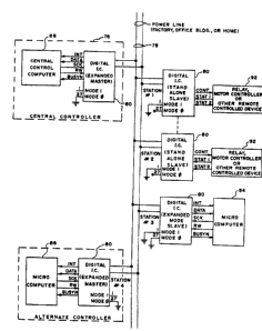
Referring now to FIG. l, there is shown a
general block diagram o~ the communication networ~
wherein a central controller indicated generally at
76 can transmit messages to and receive messages from
a large number of remote stations over a conventional
power line indicated generally at t8. The basic
building ~lock of the communication network is a
small, low cost digital IC, indicated generally at 80,
which is arranged to be connected to the power line
~ so that it can receive messages from the central
controller at 76 and transmit messages to the central
controller over tbis line.
~ he digital IC 80 is extremely versatile
and can be readily adapted to different modes of
operation by simply establishing different connec-
tion~ to two of the external pins of this device.
More particularly, as shown at remote stations ~l and
~2 in FIG. l, the digital IC 80 may be pin configured
to operate in a stand alone slave mode in which it is
arranged to control an associated relay, motor con-
troller or other remote control devlce, indicated
generally at 82, by sending a control output signal
14 ~30317~ s 1930
(COUT), to the controllea device 82. In the stand
alone slave mode, the digital IC 80 can also respond
to an appropriate command from the central controller
76 by transmittinq a message back to the controller
76 over the power line 7~ in which the status of 2
terminals associated with the controlled device 82,
identified as STAT l and STAT 2, are given. Each of
the digital IC's 80 is provided with a 12 bit address
field so that as many as 4,095 of the devices 80 may
Oe individually associated witb different relays,
motor controller~, load management terml~als, or
other controlled devices at locations remote from the
central controller 76 and can re3pond to shed load or
restore load commands transmitted over the power line
7~ by appropriately changing the potential on its
COUT line to the controlled device 82.
The digital IC ~0 is also arranged -~o that
it can be pin conigured to operate in an expanded
slave mode as shown at station ~3 in FIG. l. In the
expanded slave mode the digital IC is arranged to
respond to a particular command from the central con-
troller 76 ~y establishing an interface with an as-
sociated microcomputer indicated generally at 84.
More particularly, the expanded slave device 80 re-
sponds to an enable interface instruction in a mes-
sage received from the central controller 76 ~y pro-
ducing an interrupt signal on the INT line to the
microcomputer 84 and permitting the microcomputer 84
to read ~erial data out of a buffer shift register in
th~ digital IC 80 over the bi-directional DATA line
in response to qerial clock pulses transmitted over
the SCK line from the microcomputer 84 to the digital
IC 80. The digital IC 80 is al50 capable of respond-
ing to a signal on the read write line (RW) from the
microcompueer ~4 ~y loading serial data into the buf-
fer 3hift register in the device 80 from the DATA
line in coordination with serial clock pul es suppli-
15 ~3~31~8 51930
ed over the SCX line from the microcomputer 84. Thedigital IC 80 is then arranged to respond to a change
in potential on the RW line by th~ microcomputer ~4
by incorporating the data supplied to it from tne
microcomputer 84 in a 33 ~it message which is format-
ted to include all of the protocol of a standard mes-
~age transmitted ~y the central controller 76, This
33 bit message in the correct format i5 then trans-
mitted by the IC ~0 over the power line 7~ to the
central controller. As a result, the expanded slave
device 80 enables bi-directional communication and
transfer of data between the central controller 76
and the microcomputer 84 over the power line 78 in
response to a specific enable interface instruction
initially transmitted to the expanded slave device ~0
from the central controller 76. Since the interface
has ~een established between the devices 80 and 84
this interface remain~ in effect until the digital IC
receives a message transmitted from the central con-
troller 76 which includes a disa~le interface in-
struction or the expanded slave device 80 receives a
message from the central controller which includes a
command addressed to a different remote station. In
either case the interface between the network and the
microcomputer 84 is then disabled until another mes-
sage is transmitted from the central controller to
the expanded slave device 80 which includes an ena~le
interface instruction. The expanded slave device 80
al~o ~ends a busy signal over the BUSYN line to the
mi~rocomputer 84 whenever the device 80 is receiving
a message ~rom the network 78 or transmitting a mes-
sage to the network 78. The BUSYN signal tells the
microcomputer 84 that a message is being placed on
the network 78 ~y the central controller 76 even
though control of the buffer shift register in the ex-
panded slave device 80 has been chifted to the micro-
computer 84.
~303178
16 51930
The digital IC ~0 may also be pin configur-
ed to operate in an expanded master mode as indicated
at ~tation ~4 in FIG. l. In the expanded master mode
the device 80 is permanently interfaced with a micro-
computer 86 so that the microcomputer 86 can operateas an alternate controller and can send shed and re-
store load messages to any of the stand alone slaves
80 of the communication network. The microcomputer
86 can also establish communication over the power
line 78 with ehe micrcomputer 84 through the expanded
slave IC device 80 at station ~3. To establish such
two way communication, the microcomputer 86 merely
transmits data to the expanded master device 80 over
the bidirectional DATA line which data include~ the
address of the expanded slave device 80 at sta,tion ~3
and an enable inter~ace instruction. The expanded
master 80 includes this data in a 33 ~it message for-
matted in accordance with the protocol required by
the communication network and transmits this message
over the power line 7~ to the expanded slave 80 at
station #3. The expanded slave 80 at this station re-
spondq to the ena~le inter~ace instruction by esta~-
lishing the above descri~ed interface with the micro-
computer 84 after which the bidirectional exchange of
data ~etween the micrcomputers ~4 and 86 is made pos-
sible in the manner described in detail heretofore.
A digital IC 80 which is pin configured to
oper~te in the expanded master mode may also be used
a~ an interface between a central control computer
B8, wh~ch may comprise any microcomputer or main
frame computer, which is employed to control the re-
mote stations connected to the central controller 76
over the power line 78. Since each of the digital
IC's 80 puts out a BUSYN signal to the associated
computer when it is ei~her receiving or transmitting a
mes~age the pre~ent communication and control ~ystem
permits the u~e of multiple ma~ters on the same
1~03~78
17 51930
network. Tbus. considering the central controller 76
and the alternate controller at tation ~4 which is
operating in the expanded master mode, each of these
ma-qter~ will ~now when the other is transmitting a
message by monitoring his BUSYN line.
It will thus ~e seen that the digital IC 80
is an extremely versatile device which can be used as
either an addressable load controller with status
reply capability in the stand alone slave mode or can
~e used as either an addressable or non addres~a~le
interface ~etween the network and a microcomputer so
as to ena~le the bidirectional transmission of data
between any ~wo microcomputer control unit~ such as
the central controller 76 and the remote statlons t 3
and ~4.
Network Communications Format
All communications on the network 78 are
asynchronous in nature. The 33 bit message which the
digital IC ~0 is arranged to either transmit to the
network 7~ or receive from the networks 7~ is speci-
fically designed to provide maximum security and pro-
tection against high noise levels on the power line
78 while at the same time making possible the estab-
lishment of înterfaces between different microcompu-
ters as described heretofore in connection with FIG.1. The 33 bit mes~age has the format shown in FIG. 2
wherein the 33 bits ~0-B32 are shown in the manner in
which they are stored in the shift register in the
digital IC ao i.e. reading from right to left with
the least significant bit on the extreme right. Each
33 bit message begins with 2 start ~its B0 and Bl and
ends with 1 stop bit B32. The start bits are definPd
as logic ones "1" and the stop bit i5 defined as a
logic ~on. In the disclosed communication and con-
trol qy~tem a logic 1 is defined as carrier preqentand a loqic 0 is defined aq the absence of carrier
for any of the modulated carrier ~aud r~tes.
1l~303 1 7 8 51930
The next ~it B2 in the 33 ~it message is a
control bit which defines the meaning of the succeed-
ing ~e sage bits B3 theough B26, which are referred
to as buffer bits. A logic ~l~ control bit means
that the buffer bits contain an addre3s and an in-
struction for the digital IC 80 when it is configur-
ed to operate in either a stand alone slave moae or
an expanded slave mode. A logic ~0~ control bit B2
means that the bufer bits B3 through B26 contain
data intended for an interfaced microcomputer ~uch as
the microcomputer 84 in FIG. l.
The next four bit~ B3-B6 a~ter the control
bit 2 are instruction bits if and only if the pre-
ceeding control ~it is a ~l~. The instruction bits
~3 - B6 can ~e decoded to give a number of different
instructions to the digital IC 80 when operated in a
slave mode, either a stand alone slave mode or an
expanded slave mode. The relationship ~etween the
instruction bits B3 - B6 and the corresponding in-
struction is shown in FIG. 3. Referring to thisfigure, when instructions ~its B3, B4 and 85 are all
~0~ a shed load instruction is inaicated in which the
digital IC 80 resets its COUT pin, i.e. goes to logic
zero in the conventional sense so that the controlled
device 82 is turned off. An X in ~it position B6
means that the ~hed load instruction will ~e executed
independently of the value of the B6 ~it. However,
if B6 i3 a Ul~ the digital IC 80 will reply ~ac~ to
~he central controller 76 with information regarding
the ~tatus of the lines STAT l and STAT 2 which it
receives from the controlled device 82. The format
of the reply message is shown in FIG. 4, as will ~e
described in more detail hereinafter.
When instruct~on bits B3-B5 are lO0 a re-
store load instruction is decoded in re~ponse towhich the digital IC 80 ~cts its COUT pin and pro-
vides a logic one on the COUT line to the controlled
131)3~8
19 51930
device 82. Here again, a ~1~ in the B6 bit instructs
the device 80 to reply bac~ with status in~ormation
from the controlled device 82 to indicate that the
command has been carried out.
S When the instruction bits B3-B5 are 110 an
enable interface instruction is decoded which in-
structs an expanded slave device, such as the device
80 at station ~3, to e~tablish an interface with an
associated microcomputer such a the microcomputer
84. The d~gital IC 80 responds to the enable inter-
face ins~ruction by producing an interrupt signal on
the INT line after it has received a message from the
central controller 76 which contains the enabl~ in-
terface instruction. Further operation of the digi-
tal IC ~0 in esta~lishing this interface will be de-
scribed in more detail hereinafter. In a similar
manner, the instruction 010 instructs the digital IC
80 to disable the interface to the microcomputer 84
so that thic microcomputer cannot thereafter communi-
cate over the network 78 until the digital IC 80
again receives an enable interface instruction from
the central controller 76. In the disable interface
instruction a al~ in the B6 bit position indicates
that the expanded slave device ~0 should transmit a
reply bac~ to the central controller 76 which will
confirm to the central controller that the micro
interface h~s been disa~led by the remote device 80.
The B6 Dit for an enable interface instruction is
alway zero 50 that the digital IC ~0 will not trans-
mit b~ck to the central controller data intended for
the microcomputer 84.
If ~its B3-~5 are 001 a block shed instruc-
tion Ls decoded. The block shed instruction is in-
tended for stand alone slavec and when it is received
the stand alone slave ignores the four LSB's of
its addr~s~ and execute~ a ~hed load operation.
Accordingly, the block shed instruction per~its the
~3V3~78
20 51930
central controller to simultaneously control 16 stand
aione slaves with a single transmitted mes3age so
that these slaves simultaneously d.~le their asso-
ciated controlled devices. In a similar manner if
the instruction bits B3-BS are 101 a bloc~ restore
instruction is decoded which is ~imultaneously inter-
preted by 16 stand alone slaves to restore a load to
their respective controlled devices. It will be
noted that in the bloc~ shed and blocK restore in-
structions the B6 bit must ~e "0" in order for the
instruction to ~e executed. Thi~ is to prevent all
16 of the instructed stand alone slave~ to attempt to
reply at the same time.
If the 33-B5 bits are Qll a scram instruc-
lS tion is decoded. In response to the scram instruc-
tion all stand alone slaves connected to the networ~
78 disregard their entire address and execute a shed
load operation. Accordingly, by transmitting a scram
instruction, the central controller 76 can simultane-
ously control all 4,0Y6 stand alone slaves to shed
their loads in the event of an emergency. It will be
noted that the scram instruction can only be executed
when the B6 bit is a "on.
If the B3-BS bits are all "1" a status in-
struction is decoded in which the addressed stand
alone slave takes no action with respect to its con-
trolled device but merely transmits bac~ to the cen-
tral controller 76 status information regarding the
a~sociated controlled device 82.
Returning to the message ~it format shown
in FIG. 2, when the received message is intended for
a stand alone slave, i.e. the control ~it is "i",
bits B10-B21 constitute address bits of the address
as~igned to the stand alone slave. In this mode bits
B7-B9 and bits B22-B25 are not used. However, when
an enable interface instruction is given in the ex-
panded mode, bits B7-B9 and B22-B26 may contain data
1303178
21 51930
intended for the associated microcomputer 84 as will
be des~ri~ed in more detail hereinafter.
Bits B27-831 of the received message con-
tain a five bit ~CH error checking code. This BCH
code is developed from the first 27 bits o~ the 33
bit received message as these Eirst 27 bits are
stored in its serial shift register. The stand alone
slave device 80 then compares its computed BCH error
code with the error code contained in bits B27-B31 of
the received message. If any bits of the ~C~ error
code developed within the device 80 do not agree with
the corresponding bits in ~he error code conta$ned in
~its B27-B31 of the received message an error in
transmis~ion is indicated and the device 80 ignores
the message.
FIG. 4 shows the message format of the 33
bit message which is transmitted by the stand alone
slave 80 back to the central controller in response
to a reply request in the received message i.e. a ~l"
in the ~6 ~it position. The stand alone slave reply
message has the identical format of the received mes-
sage shown in FIG. 2 except that ~its B25 and B26
correspond to the status indication on STAT 1 and
STAT 2 line received from the control device 82.
~owever, since B25 and B26 were not used in the re-
ceived message whereas they are employed to transmit
information in the reply message, the old BCH error
checking code of the received message cannot be used
in transmitting a reply back to the central control-
ler. The stand alone slave device 80 recomputes afive bit BCH error code based on the first 27 bits of
the reply me-~sage shown in FIG. 4 as these bits are
being shipped out to the network 78. At the end of
the 27th bit of ~he reply message the new BCH error
code, which has been computed in the device 80 DaSed
on the condition of the status bits B25 and B26, is
then added on to the transmitted mescage after which
~303178
~2 51930
a stop bit of 0 is added to complete the reply mes-
s~ge bac~ to the central controller.
Fig. 5 shows the format of a second message
transmitted to a digital IC 80 operating in an exp-
anded mode, it ~eing assuming that the first messageincluded an enable interface as discussed previously.
In the format of Fig. 5 the control ~it is "0~ which
informs all o the devices 80 on the power line 78
that the message does not contain address and in-
struction. The next 24 ~its after the control ~itcomprise data to be read out o~ the ~ufer shift reg-
ister in the device ~0 ~y the assoclated microcompu-
ter 84.
In the illustrated embodiment the digital
IC 80 is housed in a 28 pin dual in line package.
Preferrably it is constructed from a five micron
silicon gate CMOS gate array. A detailed signal and
pin assign~ent of the device 80 is shown in FIG. 6.
It should ~e noted that some pins have a dual func-
tion. For example, a pin may have one function in
the stand alone slave configuration and another func-
tion in an expanded mode configuration. The follow-
ing is a ~rief deYCription of the terminology assign-
ed to each of the pins of the device ~0 in FIG. 6.
TX-the transmit output of the device ~0.
Transmits a 33 bit message through a suita~le coupl-
lng network to the common data line ~8.
~ X-the receive input o~ the device 80. All
33 bit network transmissions enter the device through
thi~ pin .
RESTN-the active low power on reset input.
Resetc the internal registers in the device 80.
Vdd~the power supply input of +5 volts.
Vss-the ground reference.
XTALl and XTAL2 - the cryst~l $nputs. A
3.6864 mH~ + 0.015~ crystal oscillator $s required.
1303178
23 51930
~aud 0 and Baud l-the baud rate select in-
puts.
A0-A8 - the least significant address ~it
pins.
A~/CLK - dual function pin. In all ~ut the
test mode~ this pin is the A9 address input pin. In
the test mode this pin is the cloc~ strobe output of
the digital demodula~or in the device 80.
A10/DEMOD - a dual function pin. In all
but the test mode thi~ pir 5,1~ ~e A10 address input pin.
In the test mode this i ~. iQ the demodulated output
(DEMOD) of the digital ~emodulator in the device 80.
All/CD - a dual function p$n. In all put
the test mode this pin is the All address input pin.
In the test mode this pin is the receive word detect
output (CD) of the digital demodulator in the device ~0.
BUSYN/COUT - a dual function output pin.
In the expanded slave or expanded master modes th~ 5
pin is the 8USYN output of the micro interface. In
the stand alone slave mode this pin is the switch
control output tCOUT).
INT/TOUT - a dual function output pin. In
the expanded master or expanded slave modes this pin
is the interrupt output tINT) of the micro interface.
In the stand alone slave mode this pin is a timer
control pin ~TOUT).
SC~/STATl - a dual functlon input pin. In
the expanded master and expanded slave modes this pin
is the ~erial cloc~ (SCK) of the micro interface. In
th~ s~and alone slave mode it is one of the two
status $nputs (STATl).
RW/STAT2 - a dual function input pin. In
the expanded ma ter or expanded slave mode this pin
i- the read-write control line of the micro inter-
face IRW). In the stand alone ~lave it is one of the
two 8tatu3 inputs ISTAT2).
i303178
24 51930
DATA/TIMR - a dual ~unction pin. In the
expanded ma~ter or expanded slave mode9 this pin is
the bidirectional data pin (DATA) of the micro inter-
face. In the stand alone slave ~ode this pin is a
timer control line (TIMR).
All input pins of the device 80 ar~ pulled
up to the +5 ~ive volt supply Vdd by internal 10~
pull-up resistors. Preferably these internal pull-up
resistor~ are provided by suitably biased transi~tors
within the device 80, a-~ will ~e readily under~tood
by those skilled in the art.
As discussed generally heretofore the digi-
tal IC 80 is capable of operation in ~everal differ-
ent operating modes ~y simply changing external con-
nections to the device. The pins which control themodes of operation o~ the device 80 are pin~ 1 and
27, identified as mode 1 and mode 2. The relation-
ship between these pins and the selected mode i~ a
follows:
MODE 1 MODE 0 SELECTED MODE
o o expanded slave
0 1 stand alone slave
1 0 expanded master
1 1 test
When only the MODE 1 pin is grounded the
MODE 0 pin assumes a logic ~1" due to its internal
puli up re~istor and the digital IC 80 is operated in
the stand alone slave mode. In this pin configura-
tion the digital IC ~0 acts as a switch control with
~tatu~ feed bac~. The device 80 contain~ a 12 ~it
addres~, a switch control output (COUT) and two
status inputs (STAT1) and (STAT2). The addressed
device 80 may be commanded to ~et or reset the switch
control pin COUT, reply with status information from
it~ two ~tatus pins, or both. The device~ 80 may be
addresRed in block~ of 16 for one way qwltch control
commands.
~303i78
25 51930
When both the MODE 1 and MODE 0 pins are
grounded the device 8 is operated in an expanded
slave mode. ~n this pin configura-ion the device 80
contains a 12 bit address and a microcomputer inter-
face. This interface allows the central controller
76 and a microcomputer 84 tied to the device 80 to
communicate with each other. The interface is dis-
a~led until the central controller 76 enables it by
sending an enable interface command to the addressed
digital IC 80. The central controller and microcom-
puter communicate by loading a serial shi~t cegister
in the digital device 80. The central controller
does this ~y sending a 33 bit mes~age to the device
~0. This causes the microcomputer interface to in-
terrupt the microcomputer 84 allowing it to read the
shift register. The microcomputer 84 communicates
with the central controller 76 by loading the same
shift register and commanding the device ~0 to trans-
mit it onto the networ~.
When only the mode 0 pin ic grounded the
MODE 1 pin assumes a logic ~1" due to its internal
pull up resistor and the device 80 is operated in the
expanded master mode. In this mode the device 80
operates exactly like the expanded slave mode except
that the micro interface is always ena~led. Any net
work trans~i~sions that the digital device 80 receives
produce interrupts to the attached microcomputer 84,
enabllng it to read the serial ~hift register of the
device 80. AlSo the microcomputec may place data in
3Q the shift register and force the device 80 to trans-
mit onto the network at any time.
When both the MODE 1 and MODE 0 pins are
ungrounded they assume ~logic" values of ~1~ and the
device 80 i~ configured in a test mode in which some
of the externa' signals in the digital demodulator
portion of the device 80 are Drought out to pins for
test purp~ses, as will be de3cribed in more detail.
1303178
26 51930
As discussed generally heretofore the digi-
tal IC 80 is adapted to transmit messages to and re-
celve ~essages from different types of communication
network lines such as a conventional power line, a
dedicated twisted pair, or over fiber optic cables. When
the digital IC 80 i5 to work with a conventional AC
power line 78, this device is pin configured qo that
it receives and transmits data at a baud rate of 300
~its per second. Thus, for power line applications
the ~inary ~its consist o~ a carrier of 115.2 ~Hz
which is modulated by on-off ~eying at a 300 ~aud
bit rate. This ~it rate is chos~n to minimlze bit
error rates in the relatively noi y environment of
the power line 7~. Thus, for power line applications
LS the digital IC ~0 is configured as shown in FIG. 7
wherein the baud 0 and baud 1 pins of the device 80
are ungrounded and assume logic values of ~1~ due to
their internal pull up resistors. The RX and TX pins
of the device 80 are coupled through a coupling net-
work and amplifier limiter 90 to the power line~ 78,this coupling network providing ~he desired isolation
~etween transmit and received messages so that two
way communication between the digital IC 80 and the
power line 78 is permitted, as will ~e described in
more detail hereinafter. When the device ~0 is pin
configured as shown in FIG. 7 it is internally ad-
justed so that it will receive modulated carrier mes-
sages ~t a 300 baud rate. It is also internally con-
trolled so that it will transmit messages at this
same 300 baud rate.
In Fig. ~ the digital IC ~0 is illustrat-
ed in connection with a communication networ~ in
which the common data l~ne is a dedicated twisted
pair 92. Under these conditions the baud 0 pin of
the dev$ce 80 is grounde~ whereas the baud 1 pin as-
sume a logic va~ue of ~1~ due to it~ lnternal pull
up resistor. When the device 80 is pin con~igured as
i3031 78
27 51930
~hown in FIG. 8 it is arranged to transmit and re-
celve modulated carrier mecsages at a 1200 baud cate.
The 1200 ~ud bit rate is pos~ible due to the less
nol~y environment on the twisted pair 92. In the
configuration of Fig. 8 the coupling network 90 is
al~o required to couple the device 80 to the twisted
pair 92.
For high speed data co~munication the digi-
tal IC 80 is also pin con~igurable to tranqmit and
receive unmodulated data at the relatively high ~it
rate of 38.4K ~aud. When so configured the device 80
is particularly suita~le for operation ~n a communi-
cations system which employs the fi~er optic ca~les
94 (Fig. 9) as the communication network medium.
More particularly, when the device 80 is to function
with the fi~er optic cables 94 the baud 1 terminal is
grounded and the ~aud 0 terminal assumes a logic
value of "1" due to its internal pull up resistor, as
shown in FIG. 9. In the fi~er op~ic cable system o~
FIG. 9 the couplin~ network 90 is not employed.
Instead, the receive pin RX of the device 80 is
directly connected to the output o~ a fiber optic
receiver 96 and the transmit pin TX is connected to a
fi~er optic tran~mitter 98. A digital IC ~0 in the
central controller 76 is also interconnected with
the fiber optic cables 94 ~y a suitable transmitter
receiver palr 100. The fiber optic receiver 96 and
transmitter 98 may comprise any suitable arrangement
in which the RX terminal is connected to a suitable
photodetector and amplifier arrangement and the TX
terminal is connected to a ~uita~le modulaeed light
~ource, such as a photodiode. For example, the
Hewlett Pac~ard HFBR-1501/2502 transmitter receiver
pair msy ~e employed to connect the digital IC 80 to
the fiber optic cables 94. Such a transmitter-
receiver pair operate~ at TTL compat~le logic levels
1303178
28 51930
whlch are satl~factory for direct application to the
RX and TX terminals of the device 80.
In Fig. 10 a typical configuration i shown
for the device 80 when operated in the ~tand alone
clave mode. Referring to this figure. pluq 5 volts
DC i~ applied to the Vdd terminal and the Vss termlnal
is grounded. A crystal 102 operating at 3.6864 -0.015~
mHz i~ connected to the OSCl and OSC2 pin~ of the de-
vice 80. Each side of the crystal i5 connected toground thro ~h a capacitor 104 and 106 and a re~i~tor
108 is connected across the crystal 102. Prefer-
rably, the capacitors 104, 106 have a value of 33
picofar~ds and the resistor 10~ has a value of 10
megohms. The ~aud rate at which the device 80 is to
operate can be selected by means of the baud rate
switches 110. In the em~odiment of FIG. 10 these
switche are open which means that the device 80 is
operating at a baud rate of 300 baud which is ~uit-
a~1e for power line network communication. The MODE1 terminal is grounded and the MODE 0 terminal is not
connected 50 that the device 80 is operating in a
stand alone slave mode. A 051 microfarad capacitor
112 is connected to the RESETN pin of the device 80.
When power i~ applied to the Vdd terminal o~ the device 80
the capacitor 112 cannot charge immediately and hence
provide3 ~ reset signal of n o" which is employed to
reset variou~ logic circuits in the digital IC B0.
Al~o, a power on reset signal forces the COUT output
o tbe device ~0 to a logic ~1~. As a result, the
controlled device, ~uch a~ the relay coil 114, i3 en-
ergized through the indicated transistor 116 whenever
power is applied to the digital IC 80. The condition
of the relay 114 is indicated ~y the status informa-
tion ~witches 118 which are opened or closed inaccordance with the sign~ supplied to the controlled
relay 114. $wo status information ~witche~ are pro
i303178
29 51930
vided for the two line9 STATl and STAT2 even though
only a~single device i5 controlled over the COUT con-
trol line. Accordingly. one status line can ~e
conn~cted to the COUT line to con~irm that the COUT
signal was actually developed and the other status
line can be connected to auxiliary contact~ on the
relay 114 to con~irm that the load in~truction has
actually been executed.
A series of twelve address ~witches 120 may
~e selectively connected to the address pins AO-A11
so as to provide a digital input signal to the
address comparison circuit in the digital IC 80. Any
address pin whicb i~ ungrounded by the switche~ 120
assumes a logic "1~ value inside the device ~0
through the use of internal pull up re3i~tor~ on each
address pin. In this connection it will be understood
that the device 80, and the external component~ as-
sociated with it, including the coupling netvor~ 90
may all ~e assem~led on a small PC ~oard or card
which can be associated directly with the controlled
device such as the relay 114. Fur~hermore, the digi-
tal IC 80 and its associated components can be of ex-
tremely small size so that it can be actually located
in the housing o~ the device which it controls.
Thus, if the device ~0 is employed to control a relay
~or a hot water heater or freezer in a residence, it
may be a~ociated directly with such relay and re-
ceive mes~age~ or controlling the relay over the
house wiring of the residence. If the controlled de-
vice doe~ not include a five volt source for poweringthe digital IC 80. the coupling networ~ 90 may pro-
vide such power directly from the power line 78, as
will be de~cribed in more detail hereinafter.
In some situations it 1~ desiraDle to pro-
vide a varia~ly timca shed load feature ~or particu-
lar ~tand alone ~lave application. For ~xa~ple. lf
the digital IC ~0 i9 employed to control a hot water
~3303178 51930
heater or reezer, it may be controlled from a cen-
tral controller 30 that the freezer or hot water
heater may be turned off (shed loa~ instruction) dur-
ing peak load periods in accordance with predetermin-
ed time schedules. Under these conditions it would
be desirable to provide a varia~ly timed facility for
cestoring power to the controlled freezer or hot
water heater in the event that the central controller
did not transmit a message instructing the digital IC
~0 to restore load. ~uch a varia~ly timed shed load
feature may be provided in a simple manner by
employing the arrangement shown in FIG. 11 wherein a
variable timer 130 is associated with the digital IC
80. The varia~le timer 130 may comprise a commercial
type MC14536 device which is manufactured by Motorola
Inc and others.
In the arrangement o~ FIG. 11 the COUT line
of the digital IC 80 is connected to the reset pin of
the variable timer 130 and is also connected to an
internal NOR gate U625 of the device 80 whose output
is inverted. The TOUT output line o~ the device 80
is connected to the cloc~ inhibit pin of the timer
130 and the decode output pin of this timer is
connected to the TIMR input pin of the device 80.
The device 80 in Fig. 11 is also conencted in the
stand alone slave mode of FIG. 10 in which ~ode the
TOUT and TIMR lines are enabled. In the embodiment
of FIG. 11 the controlled relay 114 is connected to
the TOUT line rather than to the COUT pin of the
device 80. The timer 130 has an internal cloc~ whose
frequency can be determined by the external resistors
132 and 134, and the capacitor 136 as will ~e readily
understood by those s~illed in the art. In addition,
t~e timer 130 has a num~er of timer input terminalq
A, B, C and D to which shed time select switches 138
may ~e selectively connected to estaDli~h a desiced
variable timer interval.
i303178
31 51930
When power is applied to the digital ~C 80
in FIG. 11 a power on re~et produces a logic ~1~ (re-
store load state) on the COUT pin. This signal is
applled to the reset terminal of the timer 130 forc-
S ing the timer to reset and its decode output pin low.
This decode output pin is connected to the TIMR line
of the device 80 which is internally connected to the
NOR gate U625. Since the TOUT pin is the logical OR
of COUT and the decode output of the timer 130, upon
power on reset TOUT is a logic 1 and the relay 114 i~
in a restore load state. When the COUT line is re-
set, in response to a shed load lnstruction to the
device 80, the timer 130 is allowed to start counting
and the TOUT pin is a logic ~0" cau~ing the load to
De shed. When the timer 130 counts up to a number
determined by the shed time select switches 138 its
decode out pin goes high forcing TOUT high l.e. back
to the restore load state and inhi~iting the timer
cloc~. Accordingly, if the central controller for-
get to restore load to the relay 114 by means of anetwork message transmitted to the device 80, the
timer 130 will restore load automatically after a
predetermined time interval.
In FIG. 12 the main component parts of the
digital IC 80 are shown in block diagrsm form when
the device 80 is operated in the stand alone slave
mode and is ~rranged to receive a message transmitted
over the network 7& which includes a shed load in-
struction. The incoming message is amplified and
limited in tbe coupling networ~ 90, as will ~e de-
scribed in more detail hereinafter, and is applied to
the RX terminal (pin 6) of the digital IC 80. It
will be understood that the incoming message is a 33
bit message ~ignal having the format described in de-
tail heretofore in connection with ~ig. 2. This in-
coming message is demodulated in a digit~l demodu-
lator 150 whicn also includes the start bit detection
321 3 03 ~ 7 8 51930
and framing logic nece~sary to estaDlish the bit in-
tervals of the incoming asynchronous message trans-
mitted to the device ~0 over the network 7~. The
digital demodulator and its accompanying framing
logic will be descri~ed in more detail hereinafter in
connection with a description of the detailed schema-
tic diagram of the device 80 shown in ~IGS. 18 to 33.
The output of the demodulator 150 i5 SUp-
plied to a serial shift register indicated generally
at 152. The serial shift registe~ 152 comprises a
serieY of 26 serially connected stages the fir3t 24 of
which are identified as a buffer and store bits B3-
926 (Fig. 2) of the received me~age. The next ~tage
is the control bit register U52Y wbich ~tores the
control bit B~ (Fig. 2) of the received message. The
final stage o~ the serial hift register 152 is a
start bits register U641 which ~tores bits B0 and Bl
(Fig. 2J of the received message. In this connection
it will ~e recalled that the two start bits B0 and Bl
of each message both have a logic value of ~1~ and
hence constitute a carrier signal which extends over
two bit intervals so that both bits may be registered
in the single regiRter U641. In this connection it
should be noted that all logic components having U
numbers refer to the corresponding logic element
shown in detail $n the overall schematic of the digi-
tal IC 80 ~hown in FIGS. 18 to 33. The serial shift
register 152 1~ loaded from the left by the demodu-
lated output of the demodulator 150 which is applied
to the data input of the register 152, this data ~e-
ing clocKed into the regi-~ter 150 by means of ~uffer
shift clock pulses (BSHFCLKJ developed by the demodu-
lator 150 at the end of each bit interval in a manner
described in more detail hereinafter. Accordingly,
the incoming message 15 shifted through the regi3ter
152 until tbe start bi~3 regi~ter U641 i5 get ~y the
two ~tart bitS B0 and Bl to a logic ~1~ value. In
1303~78
33 51930
this connection it will ~e noted that the bits of the
incoming mes~age are stored in the ~uf~er portion of
the register 152 in the manner shown in FIG. 2 with
the least signi~icant blt B3 stored in the register
next to the control bit register U528.
As the demodulated data bit~ are thus being
loaded into serial ~hift register 152 they ace also
simultaneously supplied to a BCH error code computer
indicated generally at 154. More partlcularly, the
DEMOD output of the demodulator 150 i5 ~upplied
through a switch 156 to the input of th~ BCH error
code computer 154 and the output of thi~ computer i3
connected to a recirculating input through the switch
158. The BCH error code computer 154 comprises a
series of 5 serially connected shift register stages
and when the ~witches 156 and 158 are in the position
shown in FIG. 12 the computer 154 computes a 5 ~it
error code ~ased on the first 27 message ~its which
it receives from the demodulator 150 as these ~it~
are being stored in the serial shift register 152.
The clock pulses on the ~SHFCLR line, which
are used to advance the serial shift register 152.
are also supplied to a message bit counter 160. The
counter 160 i5 a six stage counter which develops an
output on its end-of-word (EOW) output line when it
counts up to 32. In this connection it will ~e
-noted that by u-~ing two logic n ln S tart bi~s which
are counted as one, the total message length may be
counted by digital logic while providing lncreased
noi~e immunity by virtue of the longer start bit in-
terval.
The message bit counter 160 also sets a
latch at the end of the 26th mes~age ~it and devel
OpeB an enabling signal on it~ GT26 (greater than 26)
output line. The GT26 signal control~ the 3witches
156 and 158 ~o that a~ter ehe 26th mes~age ~ie the
DEMOD output of the demodulator 150 ~g suppl~ed to a
3 4~30~178 51930
BCH co~parator 162 to which comparator the output of
ehe 8C~ error code computer 154 is also supplied. At
the -~ame time the sw1tch 158 is opened by the GT 26
~ignal so that the ~CH error code computed in the com-
puter 154 remains fixed at a value corresponding tothe first 26 b~ts of the recelved message. Since the
demodulator 150 continues to supply BSHFCLK pulses to
the computer 154, the BCH error code developed in the
computer 154 is then shifted out and compared ~it by
bit with the ne~t 5 ~its of the received messase i.e.
B2~-B31 (Fig. 2~ which oonstitute the BCH error code
portion o~ the incoming received message and are 8Up-
plied ~o the other input of the BCH comparator 162.
If all five bits of the BCH error code computed in
lS the computer 154 correspond with the ive bit~ of the
BCH error code contained in bits B27-a31 of the re-
ceived message the comparator 162 develops an output
on its BCHOK output line.
The digital IC 80 also includes an address
decoder indicated generally at 164 which comprises a
series of 12 exclusive OR ga~es and associated logic.
It will ~e recalled from the previous description of
FIG. 2 that bits Bll-B22 of a received message con-
tain an addre~s corresponding to the particular stand
alone slave with which the central controller wishes
to communicate. Also, it will be recalled from the
preceeding description of FIG. 10 that the address
select switche~ 120 are connected to the address pins
A0-All of tbe digital IC 80 in accordance with the
addre3s a~signed to each particular stand alone
slave. The address decoder 164 compares the setting
of the address select switches 120 with the address
stored in bits Bll-B22 of the buffer portion of the
serial shift regi~ter 152. If the two addresses co-
incide the decoder 164 develope~ an output on its ad-
dre~ O~ (ADDOK) output line.
~303178
51930
The digital IC ~0 also includes an instruc-
tlon decoder 166 which decodes the outputs of the
buffer stages corresponding to bita B3-B6 ~Fig. 2)
which contain the instruction which the addressed
stand alone slave is to execute. Assuming that ~its
B3-B5 all have a logic value of ~0~, a shed load in-
struceion ls decoded, as ~hown in FIG. 3, and the in-
struction decoder 166 produces an output on its shed
load line ~SHEDN).
10As discussed generally heretofore, the con-
trol ~it 82 of a message intended for a stand alone
slave always has a logic value of ~lu indicating that
bits 33-B26 of this me3sage include address ~itq and
instruction bits which are to ~e compared and decoded
15in the decoders 164, 166 of the digital IC 80. When
the control bit register U528 in the serial shift
register 152 is set an enabling signal is supplied
over the CONTROL output line of the register U528 to
the execute logic circuits 170. The ~CHOK output
20line of the comparator 162, the EOW output line of
the message bit counter 160 and the ADDOK output line
of the address decoder 164 are also supplied ~o the
execute logic circuits 170. Accordingly, when the
message ~it counter 160 indicates that the end of the
25message has been reached, the comparator 162 indi-
cates that all bits of the received BCH error code
agreed with the error code computed by the computer
154, the addre~s decoder 164 indicates that the mes-
sage ~ intended for this particular stand alone
30~lave, ~nd the control bit register U52~ is set, the
logic circuits 170 develop an output signal on the
EXECUTE line which is anded with the SHEDN output of
the instruction decoder in the NAND gate U649 the
output of which is employed to reset a shed load
35latch U651 and U6Y2 so that the COUT output pin of
the d~tigal IC 80 goes to a logic value of ~0~ and
power is removed f rom the controlled device 82 (Fig~
36 1303178 s 19 30
1). The stand alone slave thus executes the instruc-
tion cpntained in the received me~sage to shed the
load o~ the controlled device 82. As discussed gen-
erally heretofore when power is applied to the digi-
tal IC 80 the shed load latch is initially reset ~ythe signal appearing on the PONN line so that the
COUT line goes high when +5v. power is applied to the
device 80.
When the message bit ~6 (Fig. 3) has a
logic value of ~1~ the stand alone slave not only
executes a shed load instruction in the manner de-
scribed in connection with FIG. 12 but also i5 ar-
ranged to transmit a reply me~sage bacK to the cen-
tral controller as shown in FIG. 4. In thls reply,
message ~its 825 and B26 contain the two status in-
puts ST~Tl and STAT2 which appear on p$ns 26 and 25,
respectively, of the digital IC ~0. Considered very
generally, this reply message is developed by shift-
ing out the data which has been stored in the serial
shift register 152 and employing this data to on-off
~ey a 115.2 kHz carrier which is then supplied to the
TX output pin of the device 80. However, in accord-
ance with an importan~ aspect of the disclosed
system, the status signals appearing on the STAT 1
and STAT 2 input pins of the device 80, which repre-
sent the condition of the controlled relay, are not
employed to set the status bits B25 and B26 of the
reply message until after 15 bits have been read out
of the ~erial shift regi~ter 152. This gives consid-
erable time for the relay contacts to settle down be-
fore their status is added to the reply message being
transmitted back to the central controller.
In Fig. 13 the operation of the stand alone
slave in formatting and transmitting such a reply
meqsage Dack to the central controller is shown in
block diagram form. Referring to this figure, ~t is
as~umed that a message haQ been received ~rom the
37 1303i78 51930
centr~l controller and has been Qtored in the ~erlal
s~ift regiQter 152 in the manner described in detail
her-tofore in connection with Fig. 12. It is further
assumed that the control ~it 32 of the received mes-
-~age has a logic value of "1~ and that the message
bit a6 stored in the ~uffer portion of the register
152 has a logic value ~1~ which instructs the stand
alone slave to transmit a reply message bac~ to the
central controller. When the ~6 bit has a ~1~ value
the instruction decoder 166 produces an output s~gnal
on its COM 3 output line. Also, at the end of the
received meSQage the execute logic circuits 170 (see
Fiq. 12) produce an EXECUTE signal when the condi-
tions descri~ed in detail heretofore in connection
with Fig. 12 occur. When an EXECUTE signal i~ pro-
duced a reply latch 172 provides an output which is
employed to set a status latch 174. The Qtatus latch
174 provides a control signal to ~he status eontrol
logic 176. However, the condition of the status pins
STAT 1 and STAT 2 is not employed to set correspond-
ing ~tages of the buffer portion of the seri~l shift
register 152 until after 15 ~its have ~een shifted
out of the register 152. At that time the message
bit counter 160 provide~ an output on its ~15~ output
line which is employed in the status control logic
176 to set the corresponding stages of the buffer
portion of the regi~ter 152, these stages correspond-
ing to the location of bits ~25 and B26 in the reply
me~age after 15 bits have been shifted out of the
regi~ter 152.
Considering now the manner in which the re-
ceived message which has been ~tored in the serial
shift register 152 i~ shifted out to form a reply
me~ ~ge, it will be recalled that a message ~hich is
tran~mitted over the network 78 requires two start
bit~ h~ving a logic value of ~ owever, when the
m~3age was received it was initially detected by de-
3 8~303178 51930
tecting the presence o~ carrier on the network 78 for
a dura~ion of 2 bit~ and, hence, the two start ~lts
of the received mes~age are stored as a single ~it in
the start bit3 register U641. When a reply message
i-~ to be tran~mitted over the networ~ it i5 neces~ary
to provide a modulated carrier of two ~its duration
in response to the single start ~it stored in the re-
gister U641. To accompli~h thi~, a transmit ~trobe
signal ~TXSTB) i~ derived ~rom the reply latch 172
and is coupled through the NO~ gate U601 to reset a
one bit delay flip-flop 178 which has its D input
connected to the five volt supply Vdd. As a result
the QN output of the flip-flop 178 i~ inverted to
provide a transmit stro~e A (TXSTBA) 3ignal which
sets a transmit control latch 180. When the latch
180 is set it provides a transmit on (TXONN) signal
which is employed to release the framing counters in
the demodulator 150 so that they ~egin to provide
~SHFCLK pulses at one bit intervals.
~or the first 26 ~it~ of the reply message
the output of the ~tart bits register U641 is con-
nected throuigb a switch 190 to a transmit ~lip-flop
182 which ls al~o set by the TXSTBA signal and is
held in a ~et condition so that it does not respond
to the fir t BSHFCLK pulse which is applied to its
clock inpùt. At the same time the QN output of the
one bit delay flip-flop 178 is com~ined with ~he
first ~SHFCL~ pulse ln the NAND gate U668 so as to
provide a ~ignal which -qets a transmit enable latch
18~. When the transmit enable latch 184 is set it
provideq an enabling ~ignal to the modulator 186 to
whlch is al~o ~upplied a carrier siqnal having a fre-
qu~ncy of 115.2 ~Hz. from the digital demodulator
150. Wben the tran~mit flip-flop 1~2 is initially
~et by the TXS~BA line going low, i~ provides a 1 on
~ts Q output to the modulator 186. Accordlngly, when
the transmit ena~le latch 184 provide~ an enabling
39 ~303178 51930
signal to the modulator 186 a carrier output is sup-
plied to the TX output pin of the device 80 and is
supplied to the network 78. During this initial
transmi~sion of carrier during the ~irst start bit
~nterval the data in the serial shift regi~ter 152 is
not ~hifted out because BSHFCLg pulQes to tbe cloc~
input of the register 152 are ~locked by the NAND
gate U697. The NAND gate U697 ha~ as its second 1nput
a signal from the GT26N output line of the message ~it
counter 160 which is high until 26 ~its have been
shifted out of the register 152. ~owever, a third
input to the NAND gate U697 î~ the TXSTBA line whlch
went low when the 1 bit delay flip-flop 178 wa~ re-
set. Accordingly, the first BSHFCL~ pulse is not ap-
plied to the cloc~ input of the regi~ter 152 although
this pulse does set the tran-~mit ENABLE latch 184 and
enable carrier output to be supplied to the TX outpu~
pin for the first bi t interval. However, a ~hort in-
terval after the first BSHFCLK pulse, a delayed shift
20 clocK pulse ~DSHFHCLK), which is also developed in
the framing logic of the demodulator 150, is supplied
to the clock input of the 1 ~it delay flip-flop 178
so that the TXSTBA line goes high shortly after the
first BSHFCLK pul~e occurs. When the TXSTBA line
goes higb the BSHFCLR pulses pass through the NAND
gate U697 and shift data out of the register 152 and
~he serially connec~ed transmit flip-flop 1~2 to the
dulator 186 so that the 3ingle start bit stored in
the register U641 and the remaining bit~ B2-B26 of
the received message control the modulation of the
carrier supplied to the TX output pin. In this
connection it will be noted that the BSHFCLK pul~es
are al~o supplled to the clock input of the transmit
flip-flop 182 so as to permit the ~erial shift of
da~a to the TX output pin. However, as discu~ed
above, when the TXSTBA line i~ low it hold~ the flip-
4a ~ 03 17 8 51930
~lop 182 set so that it does not respond to the firstBSHFCLR pulse.
Considering now the man..er in which the
STAT 1 and STAT 2 status signals from the controlled
devlce are added to the reply message, it will be re-
called that the ~uffer stages are not set ln accord-
ance with the signals on the STAT 1 and STAT 2 pins
until 15 ~its have ~een snifted out of the register
152 in order to allow time for the relay contacts of
the controlled device to assume a finAl position~ It
will also be recalled that the B25 and B26 bits of
the received message are reserved for status ~its to
be added in a reply message 50 that the last active
bit in the received message is B24. When the B24 bit
has been shifted 15 times it appears in the B9 stage
of the buffer portion of the serial shift register
152. Accordingly, the conditions of the ~tatus pins
STAT 1 and STAT 2 can be set into the B10 and Bll
stages of the buffer a~ter the 15th shift of data in
the register 152. To this end, the message bit
counter 160 develops a signal on the ~15" output line
which is sent to the status control logic 176. This
logic was enabled when the status latch 174 was set
in response to a COM 3 cignal indicating that the
reply was requested. Accordingly, tne status control
logic then responds to the "15~ signal by setting
the B10 and Bll stages in accordance with the poten-
tials on the STAT 1 and STAT 2 plns. In this connec-
t~on it will be understood that the B10 and Bll
stages of the buffer initially contained part of the
addre~s in the received message. However, after ~he
received message bas been shifted 15 bits during
transmission o~ the reply message the stages B10 and
Bll are free to be set in accordance with the status
pins STAT 1 and ST~T 2 and thi-Q st~tu3 will be trans-
mitted out as a part of the reply me~sage in the B25
and B26 bit positions.
41 ~0~78 51930
As dis~ussed 9enerally heretofore, it 1s
neces~ry to compute a new BCH ercor code for the re-
ply mes~age which is transmitted bac~ to the central
controller due to the fact that the ~tatus bits B25
and B26 may now contain status information where they
were not uqed in the received message. A~ ~oon as
the transmit control latch 1~0 is set the TXO W sig-
nal controls a switch U758 so that the DEMOD output
of the demodulator 50 ia removed from the data input
of the BCH error code computer 154 and the ouptut of
the serial shift register 152 is connected to this
input through the switch 156. However, during the
initial 1 bit delay of the flip flop 178 BS~FCLK
pulses are blocked from the cloc~ input of the com-
parator 154 by the NAND gate U672 the other input of
which is the TXSTBA line which is low for th~ first
start bit. After the first BS~FCLK pulse the $XSTBA
line goes high and succeeding BSHFCLg pulses are 8Up-
plied to the computer 154. The two start ~it~ of the
transmitted message are thus treated as one bit ~y
the computer 154 in the same manner as the two ~tart
bittiv~ of a received message are decoded as one bit for
the register U641.
As the data stored in the register 152 ~s
shifted out to the transmit flip-flop 182, this data
is also supplied to the data input of the BCH error
code computer 154 through the switch 156. Also, the
recirculating input of the computer 154 is connected
th~ough the switch 158, as described heretofore in
connection witb Fig. 12. Ac.cordingly, as the 26
bit~ stored in the register 152 are shifted out of
thi~ register, the computer 154 is computing a new
BCH error code which will take into account the
status information in bits B25 and B26 thereof.
After the 26th bit has been shifted out of the regi~-
ter 152 a new five bit error code is then pre~ent in
the computer 154. When the message ~1t counter 160
42 1303~78 51930
produces an output on the GT26 llne the switches 156
a~d l5a are opened while at the same time the output
of the computer 154 i5 connected through the switch
190 to the input of the transmit flip-~lop 182 in
place of the output from the ~erial shift register
152. Since BSHCL~ pul~es are ~till applied to both
~he BC~ error code computer 154 ~nd the transmit
fllp-flop 182 the five ~it error code developed in
the computer 1~4 i5 succe~sively cloc~ed through the
transmit flip-flop 182 to the modulator 186 so as to
constitute the BCH error code portion of the tran~-
mitted reply message.
When the switch 156 i~ opened after the
26th ~it, a zero is applied to the data input of the
BCH error code computer 154 so that as the fivc bit
error code i~ shifted out of the BCH error code
computer 154 the shift regi ter st~ges are bac~
filled with zeroes. After the five error code bits
have been shifted out, the next BSHFCLK pulse clocks a
zero out o~ the computer 154 and through the transmit
flip-flop 182 to the modulator 186 to con~titute the
~32 stop bit which has a logic value of ~0~. This
completes transmi~sion of the 33 bit message onto the
network 7
When the me~sage counter 160 has counted to
32 bit~ it~ EOW line i3 supplied to a transmit off
fl1p-flop 192 so that a transmit off signal (TXOFFN)
i~ developed by the flip-flop 192. The TXOFFN signal
i~ employed to re~et the statu~ latch 174 and tne
tr~ns~it control latch 180. When the transmi~
control lat~h 180 is reset it~ TXONN output line re-
sets the transmit ENABLE latch 184. The reply latch
172 i-~ reset by timing pulses STB~D developed ~n the
fra~1ng logic of the demodulator 150, as w$11 be
described in more detail hereinafter.
43 1 3 0~1 7 851930
ExDanded Slave Mode
In Flg. 14 there is shown a block diaqram
of the digital IC 80 when operated in an expanded
slave mode and showing the operation of the dev~ce 80
in re~pon~e to an enable lnterfa~e instruction. It
will be recalled from the previou8 description that
in the expanded mode, pin 24 (DATA) of the digital IC
is used as a bi-directional serial data line ~y means
of which data stored in the serial shift regi~ter 152
may ~e re-d out by an asaociated microcomputer, ~uch
as the microcomputer 84 (~ig. l), or data from the
microcomputer can be loaded into the regi~ter 152.
Also, pin 26 o~ the device 80 act~ ~ a ~erial clock
(SCR) input by means of which ~erlal cloc~ pulse~
supplied from the associatea microcomputer ~ may be
connected to the cloc~ input of the register 152 to
control the shift of data from this register onto the
data output pin 24 or the clocking of data p~aced on
the DA~ pin into the register 152. Also, pin 25 of
the device 80 (~W) is connected as a read-write
control l}ne which may be controlled by the
as~ociated microcomputer 84 to control either the
reading of data from the register 152 or the writing
of dat~ into thls register from the microcomputer ~4.
The RW line i~ also used ~y the microcomputer 84 to
force the digital IC 80 to transmit the data present
in ~ts regi~ter 152 onto the network 78 in the 33 bit
me~ age for~at of th1~ network. Pin 9 of the deYice
functions a~ an interrupt line (INT) to the
microcomputer 84 in the expanded moae and supplies an
interrupt ~ign~l in respon~e to an ena~le interface
instruction which informs the micro 84 that a message
intended for it h~s been ~tored in the regis~er 152.
An interrupt ~ignal is also produced on the INT line
aer the de~ice 80 ha~ tran~mitted data loaded into
the rcglster 152 on~o the network. Pin 8 of ~he de-
vice B0 ~upplleg a bu3y 9ignal ~BUSYN) to the a8~0~
4~30~178 51930
ciated micro ~4 whenever a message is being received
by the .device 80 or a me~sage is being transmitted ~y
thi~ device onto the network 78.
It will ~e under9tood that the bloc~ dia-
S gram o Fig. 14 include~ only the circuit components
and loqic gates which are involved in setting up an
interface with the a~sociated micro 84 and the bi-
directional tran~mi~sion of data and control ~ignals
between the micro 84 and the devic~ 80. In Fig. 14
it is as~umed tha~ a mes~age has been received from
the central controller which contain3 an in~truction
to establish an interface with the associated micro-
computer 84 in bits B3-~5 of the me~ge and th~t the
instruction decoder 166 ha~ decoded thls instructlon
~y producing an output on its enable interface output
line (EINTN). Also, when the device 80 i5 operating
in an expanded slave mode pins 1 and 27 are grounded
and the expanded mode line EMN i~ high.
In the expanded mode of operatlon of the
digital device 80, a serial ~tatus regi~ter 200 is
employed which includes a BCH error regi~ter U642 and
an ~X/TX register U644. The BCH error register U642
is serially connected to the output of the control
~it regi~ter U52~ in the serial snift reqister 152
over the CONTROL line. The RX/TX register U644 is
serially connected ~o the output of the BCH error re-
gister U642 and the output o~ the register 644 is
~upplied througb an inverting tri-state output circuit
U762 to the bi-directional serial DATA pin 24.
It will be recalled from the previous dis-
cussion of Fig. 12 that when the dlgital devlce 80
receives a me~sage from the central controller which
includes an instruction it will not execute that in-
~truction unless the ~CH co~parator 162 (Fig. 12)
provid~s a BCHOK output wh~ch indicates that each bit
of the BCH error code ~n the rcceived me8~age com-
pares equally with the BCH error code compueed in the
45 1303~78 51930
devlce 80. The BCH error register U642 is set or re-
set ln~accordance with the BCHOK output ~rom the 8CH
comparator 162. The BCH error regiJter U642 i8 reset
when the lnitial message i5 received requesting that
S the interface be esta~ hed ~ecauqe this inqtruction
would not have been executed if it wa~ not error-
free. However, once thi~ interface has ~een ~et up
the central controller may ~end additional messages
to the microcomputer 84. During receipt of each of
these additional messages the BCH comparator 162 com-
pares the BCH error code contained in the received
me~ age with the BCH error code computed ~y the com-
puter 154 and will indicate an error by holding the
BC~OK l$ne low if all ~it~ o the two codes are not
lS the same. If the BCHOK line is low the BCH erroe
register U642 is set. However, since the interface
has already ~een set up, this second mes~age stored
in the register 152, which contains an error, may ~e
read out by the microcomputer 84 by succes~ively
clocking the SC~ line and reading the DATA line. The
pre~ence of a logic ~l~ in the BCH error register
position (second bit) of the data read out ~y the
microcomputer 84 indicates to the microcomputer 84
that an error in transmission has occurred and that
the microcomputer may wish to as~ the central con-
troller to repeat the message.
The RX/TX regi~ter U644 is employed to in-
dicate to the ~icrocomputer 84 whether or not the
serial ~hift register 152 is loaded or empty when it
receiveJ an interrupt signal on ~he I~ line. If the
regi~t~r 152 ha~ been loaded with a received message
fcom the central controller the RX/TX register U644
i~ ~et. When the micro read~ out the data stored in
the regi~er 152, the seri~l shift regi~ter 152 and
the 3erial 4tatus regi~ter 200 are back filled with
zeroe~ so that when the readout iY completely a zero
will De ~tored in the RX/TX register U644. When data
46 5~930
1303~78
1~ then loaded into the register 152 and transmit~ea
out to the networ~ thls zero remains ~tored in the
RX/TX regi~ter since it is not used during transmis-
sion~ Accordingly, when an interrupt is produced on
the rNT line after the message is transmitted, the
RX/TX register U644 remains at zero 30 as to the in-
dicate to the microcomputer th~t the message has been
sent and the register 152 i~ empty.
When the digital IC 80 i~ arranged to re-
ceive a message ~rom the network 78, the switches
U759 and U760 have the po~ition sbown in Fiq. 14 so
that the output of the demodulator 150 i5 supplled to
the data input of the serial shift reglster 152 ~nd
the received message may ~e clocked into register 152
~y means of the BSHFCLK pulses applied to the cloc~
input of the register 152. However, as soon as an
ena~le interface command has been executed in the IC
~0 control of the register 152 switches to the as50-
ciated microcomputer 84 by actuating the switche~
U759 and U760 to the opposite position. This insures
that data which has been stored in the register 152
during the received message is preserved for tran3-
mission to the microcomputer 84. It is important to
switch control of the register 152 to the microcompu-
ter 84 immediately because the micro might not be
a~le to respond immediately to its interrupt on the
INT line and an incoming message might write over the
data in the register 152 before the micro re~ds out
thi 8 data.
- 30 While the inter~ace is esta~lished to the
microcomputer 84 no more network transmissions will
~e demodulated and placed in the serial shift regis-
ter 152 until the microcomputer 84 relinquishes con-
trol. However, after control is shifted to the
microcomputer ~4, the digital demodulator 150 conti-
nue~ to demodulate network mes~ageS and when a net-
work mes~age is received produces a signal on itQ
47 13~3178 51930
RXWDETN output line. This signal i5 transmitted
t~rough th- NAND gate U671. The output of the NAND
gate U671 is inverted to produce a BUSYN output
~ignal to the a~ociated microcomputer 84. The
m~crocomputer 84 i~ thus lnformed that the device 80
has detected activity on the networK 78. This
activity might be that the central controller i5 at-
tempting to communicate with the microcomputer
through the enabled slave mode dlgital IC 80. When
the digital IC ~0 i-q tran-qmitting a me~sage bac~ to
the central controller over the networ~, a~ de~cri~ed
heretofore, the TXONN signal developed by the tran~-
mit control latch 180 (Fig. 13) al~o ~upplie~ an ~c-
tive low signal to the BUSYN oueput pin to infsrm the
microcomputer 84 tnat a me~sage is being transmit~ed
by the digital IC 80 to the central controller over
the networ~ 78.
Considering now in more detail the manner
in which control of the register 152 is shifted from
the network to the microcomputer 84, when the ena~le
interface command i~ decoded by the instruction de
coder 166 it produces an EINTN output which sets an
ena~le interface latch 202. The low output of the
latch 202 i5 co~ined with the master slave signal
EMN, which i~ high in the expanded slave mode, in the
NAND gate U749 so a~ to provide an active high signal
on the ENABLE output of the NAND gate U749 which is
one input of the NAND gate U686. Assuming that the
other input of the NAND gate U686 is also a 1, the
output of U686 goes low which iY inverted in the in-
verter U736 30 that the UPSLN line goes high. The
UPSLN line is employed to control the swi~ches U75~
and U760 and when it is high switche~ the da~a input
of the .egister 152 to the ~i-directional serial DATA
line through inverter U547 and the cloc~ input o~ the
register 152 to the ~erial cloc~ SCR line. More par-
ticularly, the UPSLN line directly controls switch
48 1 3 O 3 17 8 51930
U760 ~o that the SCK ~erial clock line i5 connected
to the~clock input of the regiqter 152. Al~o, the
UPSLN line through the inverter U547 is one input of
the NOR gate U597 the other input of which i~ the RW
line which is normally high due to an internal pull
up re~istor in the digital IC ~0. Accordingly, a
high on the UPSLN line cau~es the switch U75Y to dis-
connect the demod output of the modul~tor 150 from
the data input of the register 152 only when the RW
line i~ low.
When the microcomputer 84 wishe~ to read
the data Ytored ln the serial shlft regi~ter 152 it
does so ~y providing serial cloc~ pulses to the SCK
line. At the same time the RW line i~ high which
controls the tri-state output circuit U762 to connect
the output of the RX/TX register U644 to the bi-
directional DATA lineO Accordingly the DATA pin will
contain the ~tate of the RX/TX register U644 wbich
can ~e read by the microcomputer 84. When the UPSLN
line is high and the RW line is also high the output
of the NAND gate u6a3 is low which is inverted by the
inverter U~00 and applied as one input to the NAND
qate U801 the otber input of which is the SCR line.
The output of the NAND gate UhOl is inverted ~y
inverter U802 and is supplied to the clock inputs of
the -BC~ error regi~ter U642 and the RX/TX register
U644 so that the~e registers are also shifted ~y
pul~e~ produced by the micro on the SCX line.
Accordingly, when the micro clocks the SCR pin once
~11 of the data in the serial s~ift register 152 and
thc serlally oonnected serial statu~ regi~ter 200 is
shi~ted to the right ~o that the state of the BCH er-
ror regi~ter U642 will be pre~ent at the DATA pin.
The ~icro can then read the DATA pin again to o~tain
the Qt~te of this register. This clocking and read-
ing proce~s continues until the micro ha~ read out of
the DATA pin all of the data in the 4erial hift
49 1 30 3~7 851930
reglster 152 and the serial status register 200, In
th~s connection it will be noted that the ~tart bit
regi~ter U641 is ~ypassed during the readout opera-
eion since its informatlon is used only in transmit-
ting a message to the network. As indicated a~ove,the ~tage~ o~ the ~er~al status register 200 are in-
cluded in the chain of data which may ~e shlfted out
to the microcomputer 84 becau~e these -~tages contain
information which is useful to the microcomputer ~4.
It will also ~e noted that when an ena~le
interface signal is produced and the UPSLN line is
high, ehe RW line is also high which produce~ a zero
on the output of U683. The fact that ~oth the UPSLN
line and the RW line are high forces ~wltch U75Y to
the DEMOD position. However, since the output of
U683 is low the data input to the serial shift regis-
ter 152 will always ~e logic zeros. Accordingly, as
data is ~eing read out of the register U644 on the
DATA pin 24 the register 152 and the serial status
register 200 are being bac~ filled with zeros. After
the entire contents of these registers has been read
out the RX/TX register U644 contains a zero so that a
zero appears on the DATA pin thereafter. As indicat-
ed a~ove, when the micro receives a second interrupt
on the INT line after a message has been transmitted
the micro can read the DATA pin and verify that the
message ha been sent.
Con~iderinq now the manner in which the
stages of the ~erial status register 200 are et a~
the end of either a received message or a transmitted
message to provide the a~ove-descri~ed information to
the micro, at the end of a received message the mes-
sage bit counter 160 (F~g. 12) produces an EOW ~ig-
nal which is com~ined with DSHFCLR pulse~ from the
digital demodulator 150 in the NAND gate U647 ~Fi9.
14) ~o proYide a s~atu~ st~obe signal S~STB. The
STS~B signal is oom~ined with the ~CHOK signal in the
1303178
50 51930
NAND gate U660 so that the ~CH error register U642 is
re~et if the received ~essage was error free. The
3CROR signal is inverted in the inverter U555 whose
output i~ also combined with the S~STB signal in the
NAND gate U65~ so that the ~CH error register U642 is
set if there wa~ an error $n the received mes~age.
The STSTB signal is al~o com~ined with the E~ABLE
signal in the NAND gate U658 the output of which is
supplied to one input of a NAND gate U756 the other
input o~ whicb is the TXONN line which ls high when
the device 80 is not transmitting a message. Accor-
dingly, the RX/TX register U644 i~ ~et at the end of
a received message~
When the device ~0 transmits a mes~age to
the network the TXONN line is low so that at the end
of such transmission the STSTB signal does not set
the register U644. However, as indicated a~ove, the
register U644 is back filled with a zeco as data i~
read out or the register 152. Accordingly, the micro
can read the DATA pin, to which the output of the
regi~ter U644 is connected, and determine that a mes-
sage has been transmitted to the network and the
register 152 is empty. The register U644 is reset
when power is applied to the device ~0 and when the
interface is disa~led and the ENABLE signal disap-
pears. This ~eset i8 accomplished through the NAND
gate U657 ~nd inverter U725 which together act as an
AND gate the inputs of which are the PONN signal
and the ENABLE signal.
After the micro has read out the data stor-
ed in the ~erial shift register 152 and the status
regi~ter 200 it can either switch control bac~ to the
network ~mmediately or it can load data into the ser-
ial ~hift cegister 152 and then command the device 80
to transmit the data loaded into the regi3ter 152 on-
to the network in a 33 bit me~ age having the aDove
descri~ed network format. The micro switche~ control
51 1 3 O 31 7 ~51930
back to the network immediately by pulling the RW
line low and then high. However, the low to high
transition on the RW line, which i9 performea ~y the
microcomputer 84, occurs a~ynchronously with respect
S to the fram~ng logic in the demodulator 150. Accor-
dingly, it is important to make sure that the device
80 sees the zero to one transition which the miczo-
computer 8~ places on the RW line. This transition
i5 detected by a digital one shot 204 the two stages
of which are clocked ~y the STBDD timing pulse from
the framing logic in the demodulator 150. The stages
of the one shot 204 are re~et by the RW line 90 that
during the period when the RW line i~ held low by the
microcomputer R4 the output line RWR of the one ~hot
204 remains high. However, upon the zero to one
transition on the RW line the digital one shot 204 is
permitted to respond to the STBDD pulses and produces
an output pulse on the RWR line of guaranteed minimum
pulse width due to the fact that it is deri~ed from
the framing logic timing pulses in the demodulator
lS0. The RWR line thus goes low for a fixed interval
of time in response to a zero to one transition on
the RW line.
When the RWR line goes low it se~s a buffer
control latch 206 the QUtpUt of which is conneceed to
one input of the NAND gate U753. The other input of
the NAND gate is the RW line. Accordingly, after the
zero to 1 transition on the RW line this line is high
~o ~hat the outpùt o~ the NAND gate U753 i5 no longer
a 1~ and the UPSLN line goes from high to low. When
thi3 occur~ the switches U759 and U760 are returned
to the positions shown in Fig~ 14 sc that ~uffer con-
trol i~ shifted from the micro back to the neework.
Considering now the situation where the
micro wishes to load data into the ~erial shift
regl~ter 152 and then command ~he device 80 to trans-
mit the data in the regi~ter 152 onto the networ~,
52 13~3178 51930
the micro fir9t pull~ the RW line low whlch ena~les
data to ~e transmitted from the DATA line through the
NOR gate U5Y8, the switch U75Y, ~he NAND gate U~2
and the inverter U730 to the data input of the regis-
S ter lS2. ~8 stated previo w ly, a high on the UPSLNline has al~o cau~ed the switch U760 to conneot the
SCX serial clock line to the cloc~ input of the
register 152. ~ata rom the micro may now be placed
on the DATA pin and cloc~ed into the register 152 by
the positive clock edges of the SC~ clock pul~es.
The data entering the reg$ster 152 begins with a
control bit having a logic value of ~0~ followed by
the least significant bit of the buffer bits B3-B26
and ends up with the most significant bit of the
lS buffer bits. It should ~e noted that the micro does
not load the start bits register U641.
After this data has ~een lo~ded into tbe
register 152 the micro pulls the RW pin high. The
low to high transition on the RW line after SCK
pulses have ~een supplied to the SCK line is inter-
preted ~y the device 80 as meaning that data ha~ been
loaded into the register 152 and that this data
should now be transmitted out to the network in the
33 bit message format of the netwoe~. To detect this
condition a transmit detect flip flop 20~ is employ-
ed. More particul~rly, the cloc~ pulses developed on
the SCR line ~y the microcomputer 84, identified as
BSERCR pulse~, are applied to the cloc~ input of the
flip-flop 208 and the RW line is connected to its D
input. When the RW line is low and a BSERCX pulse is
transmltted over the SCK line from the microcomputer
84 the Q output line of the flip-flop 208 goes low.
This output is suppl1ed to the NOR gate U62B the
other input of which is the RWR line. Acoordingly,
when the RW line is again pulled high at ehe end of
tran~mission of data into the reg~ster 152 ~he RWR
line goeC low so that the output of the NOR ga~e U628
53 1303~78 5~930
goes high. Thi~ output is upplied as one input to a
N~R ~ate U601 and pa~se~ through this gate so as to
provide a low on the TXSTB line. A low on the TXSTB
lin~ cauqe~ the device 80 to transmit the data stored
in the serial ~hift register 152 onto the networ~ in
the 33 bit network format in exactly the same manner
as de~cri~ed in detail hereto~ore in connection with
Flg. 13 wherein the device 80 transmitted a reply
message bac~ to the central controller. Howev~r,
since ths micro doe~ not load data ~nto the start
bits register U641, it i3 nece~ary to ~et tbis
reg$ster before a message is transmitted. Thi~ i8
accompllshed by the TXSTBA line which goes low ~t the
beginning of a transmitted message and sets the
register stage U641 as shown in Fig. 13.
Accordingly, when the TXSTBA line goe~ high at the
end of the 1 ~it delay provided by the flip-flop 178,
the start bits register U641 i5 set and itq logic ~1~
can be shifted out to form the second half of the two
~it start signal of the transmitted message as
descri~ed previously.
When the transmie ena~le latch 1~4 (Fig.
13) is 3et at the start of transmission of this mes-
sage, the output of the NAND gate U66~ (Fig. 13) is
employed to set the transmit detect flip flop 20~
through the NAND gate U664 the other inputs of which
are the power on 3ignal PONN and the ENABLE signal.
When an STSTB 3ignal is produced at the end of ~his
transmltt~d message in response to the delayed clock
pul~es DSHFCL~ the TXONN line is low so that the out-
put of a NAND gate U687, to which these two signal~
are inputted, remains high leaving the ~uffer control
latch 206 set. This meanQ that buffer con~rol, which
wa~ switched to the networ~ ae the ~eginning of trans-
mi~sion, remains that way.
In order to signal the a-Rsociated microcom-
putor 84 that an inter~ace iS being ~et up between
1303178
54 51930
the expanded slave mode device 80 and the micro so
ehat two-way data transmi~sion over the networ~ is
possible, the device 80 produces a high on the INT
pin 9 as soon as an ena~le inter~ace inQtrUction is
decoded by the decoder 166. More particularly, when
the RX/TX regi~ter U644 i~ set at the end of a re-
ceived message con~aining the ena~le interface in-
struction, as descri~ed previously, the output of the
N~ND gate U756 is supplied as one input to the NAND
gate U1000 the other input of which is the TXONN
line. Since the TXONN line is high except during
transmission a clock pulse is supplied to the inter-
rupt flip-flop 210, also identified a~ U643. The D
line of the flip-flop 210 is connected to the 5 volt
supply so that when this flip-flop receives a cloc~
pulse its QN output qoes low, wh~cb is inverted and
supplied to the INT pin 9 of the device 80. Thls
signals the associated microcomputer that an inter-
face has ~een establisbed ~etween it and the expanded
slave device 80 so that the micro may read tbe data
stored in the serial shift register 152 from the DATA
pin and load data into this register in the manner
described in detail heretofore. As soon aQ the micro
produces the firs~ pulse on the SCK line, either in
reading data from the register 152 or writing data
into the register 152, this SCK pulse resetR the
interrupt flip flop 210 and removes the interrupt
signal from the INT line. More particularly, this
SCR pulse is suppli~d to one input of a NOR qate
U1002 the other input of which is the output of a
NAND gate U657. The output of the NAND gate U657 is
high when the interface is ena~led and power i5 on
the device 80 so the first SCK pulse resets the in-
terrupt flip flop 210.
If the micro loads the serial shift regis-
ter 152 and instructs the expand~d Ylave device 80 to
transmi~ thi R message Dack to the network t~e TXONN
i303178 519~0
line goes low during such transmission, as described
in det~ll heretofore in connection with Fig. 13.
During such transmission the NAND gates U756 and
U1000 are blocked so that the RX/TX register U644 is
not set at the end of the transmitted message. How-
ever, when the ~XONN line goes high again after the
message has been transmitted the interrupt flip-flop
210 is again clocked so that a signal is produced on
the INT pin thus signalling the micro that transmis-
sion of a message back to the central controller hasbeen completed. The fact that transmi~ion has been
completed can be verified by the micro by reading the
DATA pin which is tied to the output of the R%/TX
~egister U644 and would show a ~0~ stored in this re-
gister. In this connection it will be noted that themicro can read the DATA pin any time that the RW line
is high to enable the tristate output U762, even
though control of the register 152 has been shifted
bac~ to the network. Cloc~ing of the interrupt flip-
flop 210 is timed to coincide with the trailing edgeof the BUSYN signal on pin 9 so that the INT line goes
high at the same time that the BUSYN line goes high.
While the microcomputer 84 may be program-
med in any suitable manner to receive data from and
transmi~ data to the expanded mode slave digital IC
80, in FIG. 15 there is shown a general or high level
flow chart for the microcomputer 84 ~y means oE which
it may respond to the interface and establish bi-
directional communication with and data transmission
~0 to the networ~ 7B through the digital IC 80. Refer-
ring to tnis figure, lt i~ assumed that the as~oci-
ated digital IC 80 has received a message which in-
cludeQ an enable interface command but has not yet
produced an interrupt on the INT line. Under these
35 condition~ the RW line is high and the SCR line is
low, as indicated by the main micro program block
212. As soon as an interrupt occurs on the INT line
56 1 3 3 ~7 ~51930
the ~icro reads the DATA llne, as indicated by the
~lock 213 ln the flow chart of Fig. 15. As described
generally heretofore, the RX/TX register U644 is set
at the end of a received me~sage which include~ an
enable interface command so that the DATA line, under
these conditions is hlgh. Accordingly, the output of
the decision ~lock 214 is YES and the micro then
ceads the contents of the register 152 in the digital
IC ~0, as indicated by the process ~loc~ 215. As de-
scribed generally heretofore, the micro performs this
read out by cloc~ing the SCX line 27 times and read-
ing the DATA line on the leading edge of each SCR
pulse. After the 27th SCK pul~e a zero will be
stored in the RX/TX regiater U644, as described
heretofore in connection with Fig. 14.
A~ter it has read the contents of the re-
gister 15Z the micro has to decide whether lt wishes
to reply back to the central controller or whether it
wishes to switch control of ~he register 152 ~ack to
the networ~ without a reply, as indicated by the de-
cision bloc~ 216 in Fig. 15. Assuming first that the
micro wishec to switch control back to the network
without a reply, as indicated ~y the process bloc~
217, the micro accomplishes this ~y holding the SCK
line low and pulling the RW line low and then ~ack
high. When control is switched ~ack to the network,
the progra~ returns to the main micro program to
await the occurrence of another interrupt on the INT
line in response to a message ~rom the central con-
troller. In this connection it will ~e recalled tha~
as soon as the micro sends one pulse over the SCR
llne to read out the contents o~ the register 152 the
interrupt FF U643 is reset and the INT pin goes low
again.
After reading the content3 of the regi~ter
152, the ~icrocomputer 84 may wi~h to reply to the
central controller ~y loading d~ta into the regi3ter
57 13~3178 51930
152 and co~manding the digital IC ~0 to transmit a 33
blt me~age signal to the networ~ including th1s
dat~. Under such conditions the c~tput of the deci-
sion blocK 216 is YES and the microcomputer a4 can
load d~ta into the register 152 as indicated by the
process bloCK 219. As descri~ed he~etofore, the
micro loads d~ta into the regi~ter 152 ~y pulling the
RW line low and then serially placing data bi ts on
the DATA line and clocking each bit into the register
152 by the positive clock edges of SCR pul~es it
places on the SCR line. The data entering the chip
begins with the control ~it, ~ollowed by the least
significant ~it of the ~uf fer ~its and ends up with
the most significant bit of the buffer bits. The SCR
line ic thus cloc~ed 25 times to load the regi~ter
152.
Af ter the register 152 is loaded the micro
reads the BUSYN line to determine whether it i~ high
or low, as indicated by the decision block 220. It
will ~e recalled that the BUSYN line qoes low if a
mes~age on the networ~ is demodulated by the digital
demodulator portion of the digital IC 80 even thougb
control of the register 152 has been shifted to the
micro computer 84. Also, a burst of noise may be in-
terpreted by the demodulator 150 as an incoming
signal. Under the~e conditions the microcomputer 84
~hould not co~mand tbe IC 80 to transmit a message
onto the network. If the BUSYN line is high the
micro then gives a transmit command to the digital IC
80, as indlcated by the process ~loc~ 221. As de-
~cri~ed heretofo~e, this command is performed by pul-
ling the RW line high after it has been held low dur-
ing the loadi~g of data into the digital IC 80. Con-
trol i8 then returned to the main micro program, as
indlc~ted in Fig. 15.
After the digital IC 80 has transmitted the
data which has been loaded into the res1~ter 152 onto
1303i" 8
58 51g30
the network 7~ it produces an interrupt high on the
INT line at the end of the transmitted message. In
response to this interrupt the data line i~ again
read by thc micco aq indicated by the bloc~ 213.
However, at the end o~ a trans~itted message the data
line i8 no longer high since the RX/TX regiqter U644
contains a zero at the end of a transmitted message,-as
described hereto~ore. Accordingly, the output of the
decision ~lock 214 is negative and the program ptO-
ceeds to the decision ~loc~ 222 to determine whether~urther transmiq~ion is required from the ~icrocompu-
ter ~4 to tne central controller. If such tran~ml~-
qion iq required, further data is loaded into the re-
gister 152, as indicated ~y the ~loc~ 219. On the
other hand, if ~o further transmi~sion i~ required
the INT line is reset as indicated by the process
~lork 222. As described generally hereto~ore, this
i5 accomplished by holding the RW line high while ap-
plying one SCK pulse to the SCK line. This single
SCK pulse resets the interrupt flip flop 210 (FIG.
14~ and removes the interrupt signal from the INT
line.
It will thus ~e seen that the present com-
munication sy~tem provides an extremely flexible ar-
rangement for bidirectional communication between thecentral controller and the microcomputer 84 through
the digltal IC ~0. After the interface is set up the
micro read~ the message transmitted from the central
controller to the IC ~0 and can either switch control
~ack to the central controller to receive another
mes3age or may transmit a mes~age of its own to the
central controller. Furthermore, the micro can send
a series of messages to the central controller by
successively loading data into the regi~ter 152 and
commanding the digital IC ~0 to transmit thiq da~a
b~ck to the central controller, a~ indicated by
blocks 219, 220 and 221 in Fig. 15. In this connec-
~303~8
59 51930
tion it will be understood that after the interfaceis initlally set up in the first message transmitted
by the central controller, subsequent messages from
thi3 central controller to the micro use all 24 buf-
fer bits as data ~its and the control bit is a ~on.
All other devices 80 on the ~ame network, whether in
the stand alone slave mode or the expanded mode, will
interpret such a message as not intended for them due
tO the fact that the control ~it is reset, even
though the data transmitted may have a pattern cor-
responding to the address of one of these other de-
vices ~0. The transmi3-~ion of data bac~ and forth
~etween the central controller and the microcomputer
8~ continues until the central controller disa~le~
lS the interface.
The.interface may be disacled by a direct
disable interface instruction to the device 80 asso-
ciated with the microcomputer, in which case the mes-
sage transmitted by the central controller will have
a control bit set (nl") and will have address bits
corresponding to the address of this device 80. The
device 80 will respond to the disa~le interface in-
struction by resetting the enable interface latch 202
~Fig. 14). In the alternative, the central control-
ler can disable the interface implicitly ~y simplytransmitting a messaqe over the network which is ad-
dressed to another a ~ital IC ~0 in which the control
bit is se~. The interfaced digital IC 80 will also
receive this message but will recognize the occur-
rence of a control bit of ~1~ together with anaddress which is not its own and will disable the in-
terface in response to t.l~ condition, as will ~e
described in more detail hereinafter. However, in
the expanded slave mode this implicit mode of disabl-
ing the interface will not be effective if a 8CHerror i9 detected in the received message. This is
done because the received message might have been in-
1303178
fi~ 51930
tended for the inte~faced microcomputer ~ut a noiseimpulse caused the control bit to be demodulated as a
~1~ instead of a zero. Under these conditions, the
BCHOK line will not go high at the end of the receiv-
ed message and this condition is used to maintain theinterface, as will be deqcri~ed in more detail here-
inafter.
ExPanded Master Mode
As discussed generally heretofore, the
digital IC ~0 may also be pin configured to operate
in an expanded master mode as indicated at station ~4
in FIG. 1. In the expanded master mode the device 80
is permanently inter~aced with a microcomputer 86 so
that the microcomputer ~6 can operate a~ an alternate
controller and can send she~ and restore load signals
to any of the stand alone slaves 80 vf the
communication networ~ if the central controller 76 i
inactive and does not place any messages on the
network. This intes~ace is permanently esta~lished
when the MODEl pin 1 of the device 80 at station ~4
is ungrounded, as shown in Fig. 1, so that the EMN
line in Fig. 14 is always low and the ENABLE line is
always held high through the NAND gate U749. The
expanded ma~ter device 80 at station #4 should have an
address which is different from the address of any of
the other devices 80 on the line 78 so as to permit
the centr~l controller to communicate with the
microcomputer 86.
The microcomputer 86 can also establish
co~un~cation over the power line 7~ with the
microcomp~ter 84 through the expanded slave IC device
-80 at station ~3. To establish such two way
communication, the microcomputes 86 merely transmits
data to the expanded master device 80 over the
bidirectional DATA line which data inclu~es the
address of the expanded ~lave device 80 at station ~3
and an enable inter~ace instruction. The expanded
61 i 30 3~ 8 51930
ma3ter 80 includes this data in a 33 bit message
formatted in accordance with the protocol required by
the communlcation netwOrK and transmits this message
over the power line 78 to the expanded slave 80 at
station ~3. The expanded slave 80 at this station
recponds to the enable interface instruction by
establishing the above descri~ed interface w~th the
microcomputer 84 after which the ~idirectional ex-
change of data ~etween the microcomputers ~4 and 86
is made possi~le in the manner descri~ed in detail
heretofore.
A digital IC 80 which is pin configured to
operate in the expanded ma-Qter mode i9 also used as
an interface between the central control computer 88,
which may comprise any microcomputer or main frame
computer, which is employed to control the remote
stations connected to the central controller 76 over
the power lines 78. The expanded master device 80
associated with the central controller 76 should also
have an address assigned to it which is different
from the address assigned to any of the other digital
IC's on the line 78, including the digital IC ~0 at
station ~4 associated with the microcomputer 86.
This is true even though the interface to the central
control computer 88 is always ena~led as discussed
previously in connection with the expanded master de-
vice ~0 at st~tion ~4.
SLnce the expanded master digital IC's 80
~3sociated with the central computer 88 and the
30 microcomputer 86 each produces a BUSYN signal when-
ever it i~ receiving a mes~age from the network, the
presently descri~ed communications and control system
permit~ the use o~ multiple masters on the same net-
work line. If, or example. the mlcrocomputer 86
wishes to cend a message to any other point in the
sy-~tem, including the central controller 76, the
microcomputer 86 can monitor its BUSYN line to see if
130317~
51930
any ~e5~age is on the networ~ at that time. In the
same manner, the central controller 76 can monitor
it~ aUSYN line before sending a message to be sure
tbe mlcrocomputer 86 is not sending or receiving a
message at that time.
~Li~ e~ g~
As will ~e recalled ~rom the preceeding
general discus~ion, the coupling network 90 provides
bidirectional coupling between the network 78 and the
digital IC ~0 which is tuned to the carrier frequency
of 115.2kHz. The coupling network 90 also provide~
amplification of the received signal and llmit~ thi~
signal in ~oth the positive and negative directions
to five volts peak to pea~ ~efore it is applied to
the RX input terminal of the device ~0. The coupling
network 90 also couples the transmitter output termi-
nal TX to the power line and drives it with suffi-
cient power to provide a signal of 1 volt run~ ampli-
tude on the power line 7~ when the device 80 ic
transmitting a message onto the networ~.
In FIG. 16 a coupling network 90 is shown
which is particularly suita~le for applications
wherein the device 80 is to be associated with a con-
trolled unit, such as a hot water heater or freezer,
in a re3idence. In such applications a +5V supply
for the device 80 i~ not usually available and the
coupling nctwork Y0 of FIG. 16 is arranged to func-
tion fro~ the conventional power line and develop a
~uitable pow~r supply for the device 80. ~eferring
to thi~ figure, the power lines 230 and 232, which
may ~e a 240 volt AC line, supply power to a load
234, which may comprise a hot water heater or freezer
ln a residence, through a power relay indicatea
generally at 236 wnich has the normally closed power
relay contacts 23~ and 240. A protective device 242
i3 connected ~etween the power 1 ine 232 and neutral,
this voltage ~ormally being 120 volts AC. A ~ull
1303178
63` 51930
wave rectifier 244 rectifies the AC voltage on the
llne 232 and the output of the rectifier 244 is
connected throuqh a diode 250, a resistor 2~a and a
filter capacitor 246 to ground so that a DC voltage of
5 approximately 150 volts is developed across the
capacitor 246.
In order to provtde a suitable voltage
level for energizing the device 80, the voltage ac-
ross the capacitor 246 is connected through a resis-
tor 252 to a Zener diode 254 across which a voltage
of + 10 V. is developed, a capacitor 256 being oon-
nected across the Zener diode 254 to provide addi-
tional filtering. A voltage regulator, indicated
generally at 258, is connected across the Zener diode
254 and is arranged to developed a regulated ~5 volts
at its output which is connected to the Vdd pin 28 of
the device 80. The voltage regulator 25~ may, for
example, comprise a type LM309 regulator manufactured
~y National Semiconductor Inc.
A transformer 260 is employed to provide
~idirectional coupling between the networ~ 78 and the
device 80. The transformer 260 includes a primary
winding 262 and a secondary winding 264, the primary
winding 262 being connected in series with a capaci-
tor 266 between the power line 232 and neutral. ~he
two winding~ 262 and 264 of the transformer 260 are
decoupled so as to permit the winding 262 to func-
tion as a part of a tuned resonant circuit which in-
clude~ the capacitor 266, this resonant circuit being
tuned to the carrier frequency of 115.2 kHz. More
particularly, as shown in FIG. 16A the core structure
of the transformer 260 is formed by two sets of op-
posed E shaped ferrite core -~ections 268 and 270
opposed E shaped ferrite core sections 268 and 27û
the opposed legs of whic~ are ~eparated by a small
air gap. Preferably, these core sec~ion~ are made of
type 814E250/3E2A ferrite materlal made by the Ferrox
1303178
64 51930
Cube Corp. The winding 262 is wound on the opposed
upper leg portion~ 272 of the sections 26B and 270
and the winding 264 is wound on the bottom leg sec-
tions 274. The windings 262 and 264 are thus de-
coupled by the magnetic shunt formed ~y the opposedcenter legs of the coce sections 268 and 270 ~o as to
provide substantial decoupling between these wind-
ings. The winding 262 has an inductance of 0.2 mil-
lihenrles and consists of 100 turns of AWG~36 wire.
The winding 264 has an inductance of 7.2 millihenries
and consists of 600 turns of AWG~40 wire. The turn~
ratio ~etween the primary win~ing 262 and the secon-
dary 264 is thu~ 1:6. The air gaps ~etween the
opposed legs of the core sections 26~, 270 are pre-
fera~ly 63 mils.
The upper end o~ the winding 264 is con-
nected to the 150 volt potential developed acros3 the
capacitor 246 and the bottom end of this winding i~
connected to the collector of a high voltage NPN
transistor 2~0 the emitter of which is connected to
ground through a cmall resistor 282. Prefera~ly, the
transistor 2~0 is a type MJE 13003 which is manufac-
tured by Motorola Ins. In the alternative, a high
voltage FET type IR720 manufactured by Internaeiona
Rectifier Co. may be employed as the transistor 2~0.
The bottom end of the winding 264 is al~o connected
through a capacitor 2~4 and a pair of reversely con-
nected diode~ 286, 288 to ground.
When a modulated carrier message is trans-
~itted over the power line 232 to the remote locationof the device 80, the on-off keyed carrier signal may
have an amplitude in the millivolt range if the mes-
sage has been transmitted a su~stantial distance over
the power line. The winding 262 and capacitor 266 of
the coupling network Y0 act as a first resonant cir-
cuit whish is tuned to the carrier frequency of 115.2
kHz and has a Q of approximately 40. The winding 264
1 3 O 31 7 8 65 51930
and the capacitor 2~4 also act as a regonant circuit
which is tuned to the carrier frequency. PreferaDly,
the capacitor 266 is a polypropylene 400 V. capacitor
having a capacitance of 0.01 microfarads. The capa-
citoc 284 preferably has a value of 270 picofarads.
If the signal on the 11ne 232 has an amplitude of 10
millivolts, or example, approximately Q times the
input voltage will be developed across the winding
262 i.e. a signal of 400 millivolts a~plitude. The
signal developed actoss the winding 264 i increased
~y a factor of 6 du~ to the turn~ ratio of tbe trans-
former 260, and is coupled through the cap~citor 2~4
to a filter network which include~ the serie3 resl~-
tors 2~0, 292, and 2~4. A shunt re~istor 296 is con-
nected between the resistors 2~0 and 2Y2 and ground
and a small capacitor 298, which prefera~ly has a
value of 100 picofarads, is connected between the
junction of the resistors 292 and 294 and ground.
The output of this filter circuit is sup-
plied to one input of a comparator 300 the other in-
put of which is connected to ground. The comparator
300 may, for example, comprise one section of a quad
comparator commercial type LM239 manufactured by
National Se~iconductor, Inc. The comparator is
energized from the + 10 V. supply developed across
the Zener diode 254 and it~ output is supplied to the
RX pin 6 of the device 80. This output is also con-
nected through the resistor 302 to the five volt out-
put of the regulator 25~. A small amount of positive
feedback is provided for the comparator 300 by means
of the resistor 304 which i~ connected between the
output of the comparator 300 and the plus input ter-
~inal thereof, the resi~tor 304 preerrably having a
value of 10 megohms. The slight positive feed~ack
provided ~y the resi~tor 304 creates a small dead
band at the input of the comparator 300 ~o that a
signal of approximately 5 mill~volts is required to
1 3 0 3~ 7 8 fi6 51930
develop a signal in the output and noise voltages
~elow thls level will not ~e reproduced in the output
of the comparator 300. However, when the incoming
-~ignal exceeds a five millivolt level it is greatly
amplifled, due to the extremely high gain of the com-
parator 300 80 that an amplified carrier signal of
five volts amplitude is developed across the resistor
302 and is applied to the RX input terminal of the
device 80.
Considering now the operation of the coupl-
ing network 90 during the transmi~sion of a message
from the device ao to the network, the modulated car-
rier signal which i9 developed on the TX pin 10 o~
the device 80 i5 coupled through a capacitor 306 to
the ~ase of the t;ansistor 2dO. This DaSe is also
connected through a diode 308 to ground and through a
resistor 310 to ground. The tranRistor 280 iq a high
voltage NPN ~ransistor so that the collector of this
transi~tor can be connected through the transformer
winding 264 to the 150 volt supply appearing across
the capacitor 246. The capacitor 306 is provided to
couple the TX output o~ the device 80 to the base of
the transistor 280 because when power is applied to
the device 80 the TX output pin 10 assumes a five
volt potential which would destroy the transistor 280
if the capacitor 306 were not provided.
The transistor 280 is turned on and off ~y
the ~odulated carrier signal which is coupled to the
~a~e of this transistor through the capacitor 306 and
hence develops a voltage o~ approximately 150 volts
across the winding 264 during the carrier on portions
of the transmitted message. When the transistor 280
1s turned off there is a substantial current being
draw~ through the winding 264, which cannot change
instantaneously, so that a large bac~ EMF pul~e is
also developed across the winding 264. ~he reversely
connected diode~ 2~6 and 2~ protect the receiver in-
~303178 67 51930
put circuitry in both polarities from the high vol-
tage pulses which are developed across the winding
264 during the transmit mode. He~ever. it will be
under3tood that the diode~ 286 and 2a8 do not conduct
for small amplitude signals and hence the received
carrier signal may be coupled through the capacitor
284 to the comparator 300 without interference from
the diodes 286 and 288.
The large carrier voltage developed across
the winding 264 is ctepped down in the transformer
260 and drives the power line 232 so that the 33 bit
message developed by the device 80 may be tran~mltted
over a substantial distance to the central control-
ler. At the carrier frequency the power llne 232
will have a very low impedance cf approximately 10
ohms whereas the reactance of the capacitor 266 is
about 300 ohms at the carrier frequency. According-
ly, the power line is essentially driven in a current
mode.
Considering now the manner in which the de-
vice 80 controls the relay 236 and its associated
load 234 in response to a shed load instruction, the
relay 236 is provided with a high current coil 320
which controls the high current relay contacts 23R,
240, the coil 320 ~eing connected in series witb the
norm211y closed contacts 322 and an SCR 324 to
ground. The other side of the relay coil 320 is con-
nected to the unfiltered full wave rectified output
of th~ rectifier 244. A relatively low current hold-
ing coll 326 i~ also connected from this point to the
drain electrode o~ an FET 328 the source of wbich ~s
connected through the resistor 330 to ground. The
COUT pin 8 of the device 80 is connected to the gate
electrode of an FET 332 the drain electrode of which
is connected to the ~5 V. ~upply through the resi~tor
334 and the source is connected to ground. The drain
130317~ 8 51930
o~ the FET soUrCe i5 connectea to the gate of the FET
328.
When power is applied to the device 80 the
COUT pin goes high which causes the FET 332 to con-
S duct and the voltage developed across the resi~tor
334 holds the FET 328 nonconductive. Accordingly,
there is no current flow through the resistor 330 and
the SCR 324 is held o~f. When a shed load instruc-
tion is received by the device 80 the COUT line goes
low which turns off the FET 332 and cause~ the FET
32~ to conduct. The voltage produced acros~ tbe re-
sistor 330 turns on the SCR 324 90 that the relay
coil 320 is energized and opens the main relay con-
tacts 238 and 240. At the same time, the normally
closed contacts 322 in series with the coil 320 are
opened. However, since the FET 328 is conducting the
celay coil 326 is energi2ed and holds the contacts
238, 240 and 322 open. However, the coil 326 has an
impedance su~stantially greater than the coil 320 so
that only a small current is required to hold the
contacts of the relay 236 open. When a restore load
instruction i5 received by the device 80, the COUT
line again goes high and the FET is rendered noncon-
ductive 50 that the coil 326 is no longer energized
and the normally closed contacts of the relay 236 are
again closed. Since the relay 236 has no auxiliary
contact to provide status feedbac~, the STATl and
STAT2 p~ns 26 and 25 are connected back to the COUT
pin 8 of the device 80.
If it is desired to have a varia~le time
out feature, as discus~ed in detail heretofore in
connection with Fig. 11, the TOUT pin g and the TIMR
pin 24 of the device 80 in Fig. 16 may b~ connected
in the manner shown in Fig. 11 to provide a varia~le
time out feature in association with tbe relay 236.
It will be under~tood that the coupling
network ~0 can be of very small phy~ical si2e due to
i303178
69 51930
the fact that the coupling trans~ormer 260 is rela-
t-~vely small. The coupling networ~ 90, the device 30
and the control devices 332, 32~ and 324 may all be
located on a small circuit ~oard which can ~e mounted
within the housing of the relay 236 so as to provide
an addre-~a~le relay in a simple and economical man-
ner. Furthermore, existing relays can be converted
into addressable relays ~y simply installing ~uch a
~oard and maxing apprspriate connections to the power
line.
It will ~e appreciated that in many in-
stances the controlled device associated with the
digital IC 80 will have a low voltage D.C. power sup-
ply which is provided for other logic circuit3 in the
controlled device. In such instance, the coupling
network of Fig. 16 can be modified a~ shown in Fig.
17 to operate directly from a low voltage D.C. power
source. Referrinq to thi~ figure, only the portionQ
of the networ~ of Fig. 16 are shown which are chang-
ed from the arrangement of Fig. 16. Specifically,
the upper end of the winding 264 is connected to a
+24 volt supply (assumed to be available from the
controlled device) and the bottom end of the winding
264 is connected through a resistor 340 to the drain
electrode of an FET 342 the source o~ which is con-
nected to ground. Preferably the FET is a power FET
commercial type 2N6660. The gate of the FET 342 is
connected to ground through the diode 308 and through
the capacitor 306 to the ~X terminal of the device
80. The drain of the FET 342 is also coupled through
a diode 344 and a resi~tor 346 to a light emitting
diode 34~. In the circuit of Fig. 1~ the voltage
regulator 253 and comparator 300 are of a suitable
commercial type to be energized directly from the +24
V. supply. Since a lower D.C. voltage is availa~le
in the cir~uit of Fig. 17 both of the winding~ 262
and 264 of the transformer 260 of Fig. 17 have the
1303178
70 51930
3ame number of turns, i.e. 100 turnC of AWG ~36 wire,
and the capacitors 266 and 284 are both O.Ol ufd.
capacitors.
In operation, the circuit of Fig. 17 re-
ceive~ an on-of modulat~d carrier signal from the
power line 78 which is coupled through the transform-
er 260 without step up becau~e both windings 262 and
264 have t~e same num~er of turns. The signal deve-
loped across the winding 264 i~ coupled through the
capacitor 2~4 and the input filter and comparator
300, as described in connection with Fig. 16, to the
RX terminal of the device 80. In the transmit mode
the modulated carrier signal on the TX ter~inal is
supplied through the capacitor 306 to the gate of the
FET 342 so as to turn this device on and off which
produces a modulated carrier current in the
transformer winding 264 which iq tran~mitted to the
power line 78. Since the windings 262 and 264 have
the same num~er of turns in the embodiment of Fig. 17
there is no step down of the transmitted signal in
passing through the transformer and hence the level
of the transmitted message in the power line 7~ is
a~out the same as the em~odiment of Fig. 17 even
though the 24 V. supply is approximately one sixSh of
the +150 V. sup~ly in the embodiment of Fig. 16.
The LED 348 will indicate the periods during whicn
the dev$co 80 is transmitting a message to the
network 78.
F$gs. l8 to 33, inclusive, when arranged in
the manner shown in Fig. 34, comprise a detailed
schematic diagram of the digital IC 80 described
generally heretofore. Generally speaking, in this
schematlc d$agram the logic s$gnals which are deve-
loped at the outputs of various portions of the
schematic are given a letter ab~reviat~on which ends
with ~N~ whenever that particular qignal is an active
13~3178 71 51930
low output. Otherwise the signal is active high.
DiqitaL Demodulator 150
Considering now in more detail the digital
rece~ver-demodulator 150 and its associated start ~it
S dctection and framing logic, it should first ~e
pointed out that while this demodulator i~ particu-
larly quitable for demodulating power line carrier
information in high noise environments and lends it-
self to implementation in digital large-scale inte-
gration circuitry, such as the device 80, this de-
modul~tor iq o~ broad general application and can be
used wherever it is required to demodulate ASK
modulated binary data. The demodulator may ~e u~ed
~y itself since it is readily implemented in digital
logic or may be used as a part of a larger system as
in the digital IC ~0.
As discussed generally heretofore, the re-
ceiver-demodulator 150 is arranged to demodulate daea
transmitted over a power line. Power line carrier
signals are affected Dy three types of noise:
Gaus~ian noise, coherent signals, and impulsive
noise. The carrier signal plus noise is fed into tne
digital demodulator 150 through the coupling networ~
~0 which includes an input filter which couples the
device 80 to the power line 7~, as descri~ed in de-
tail heretofore in connection with Fig. 16. This in-
put filter produces oscillations (ringing) in re-
Rpon~e to the impulsive noise input~. On the one
hand it i5 desirable to reduce the noise power ~and-
width of the input filter, i.e. high Q, while at thesame tl~e there i~ a need for a relative low Q inpue
filter to reduce the ring down time as~ociated with
inpulsive noise. The filtering action of the digital
demodulator 150 attempts to reconcile these two con-
fl1cting requirements.
A~ discussed generally heretofore, the car-
rier modulation system employed ln the digit21 IC 80
~30317872 51930
1~ on-off keying o a carrier frequency of 115.2kHz
at ~00 3aud. This modulation syste~ was chosen in
pre~erence to phase shit modula~ion at the data
rates required because of the ~ignificant phase dis-
S turbances associated with the power line 7~. Thecarrier frequency of 115.2~Hz is chosen based upon
spectural analyRes of typical power line systems and
the 300 baud bit rate is chosen to provide maximum
thcoughput with acceptable error rates.
The general appro~ch in the digital demodu-
lator lS0 is to require phase coherence in the short
term i.e. over one and a half carrier cycles, for
frequency detection, and to sen~e continued phase
coherence in the longer term i.e., l/6th of a bit, or
lS 64 carrier cycles at 300 ~aud, to di~criminate
against impulsive noise. Impulsive noise also pro-
duces frequency information that is coherent in the
short term but is not perfectly coherent in the
longer term. The reason that the longer term is not
extended to an entire bit or a longer fraction of a
bit is that the power line produces phase discontinu-
ities that are significant over the time interval in-
volved. An example of a phase discontinuity being
produced on the power line is a line impedance dis-
turbance caused by rectifiers beginning to conduct orending conduction in association with a capacitative
input filtcr. These phase discontinuities are de-
tected and lead to bit errors. 8y choosing the in-
tegration time of l/6th of a ~it, each pha e distur-
b~nce G~n lead only to a degradation of 1/6th of abit.
The digital demodulator 150 thus censes
both frequency and phase of an incoming 3ignal over a
1/6th-of a bit interval (approximately 556 micro-
secondc at 300 baud). If the input fre~uency i3 COr-
rect and maintains pha3e coherence for at least three
fourths of the 1/6th bit interval, a counter is
1303178
73 51930
incre~ented. After six of these 1-6th bit intervals
are pracessed, the counter content~ are examined. If
the counter counts up to four or more (assuming that
it started out at 0), the demodulator outputs a
demodulated logic 1. If the counter contents are
less than 4, the demodulator outputs a demodulated
loglc 0.
Referring first to the ~loc~ diagram of the
digital demodulator 150 shown in FIG. 35, an oscil-
lator and timing subsystem 400 is employed to pro-
vide all of the timing signals and strobes for the
other portions of the demodulator 150. A 3.6864 MHz
_0.015~ oscillator is employed to drive these timlng
circuit~. The carrier input ~ignal which i~ ampli-
fiad and limited in the coupling network Y0 and i5
applied to the RX input terminal of the device 80, is
inputted to a pair of carrier confirmation circuits
402 and 404, these circuits wor~ing Y0 out of pha~e
with respect to each other. Each of the carrier con-
firmation circuits 402 and 404 examines the input
signal and determines if it i5 within an acceptable
band of frequencies centerea a~out the carrier. This
is done on a cycle by cycle basis. Each carrier con-
firmation circuit has two outputs. One output pro-
duces a pul e if the signal is within the pass band
and the sampled pha~e of the input signal is a logic
1. The other produces a pulse i~ the signal is with-
in the pa~d band and the sampled phase of the input
~ignal is a logic 0. The four outputs of the carrier
confirm~tion circuits 402 and 404 are used as cloc~
inputs to a series of four pha e counters 406, 408,
410, 412 which are reset every 1-6th of a bit. At
300 baud each cit contain~ 3~4 cycles of the 115.2kHz
c~rrier. ~ Therefoce, a ~ixth of a bit cont~in~ 64
carrier cycles. Should any one of the phase counters
406-412 count up to 4~ or more, there~y indicating
phase conerence over three fourths of the sixth bit
7~ 3 0 3~ 7 8 51930
lnterval, a logic 1 is produced at the output of a
four input OR gate U166, the four inputg of which are
thc outputs of the phase counter 406-412.
The output of the OR gate U166 is connected
to the ~tart bit detection and framing logic indicat-
ed generally at 414. Considered generally, the first
logic 1 input to the circuit 414 triggers the start
~it detector. The start bit detector then releases
the reset on a counter and incrementR it at intervals
of one sixth of a ~it. This counter then counts 11
more sixth bit intervals. At the end of each sixth
~it interval the output of the OR gate U166 i~
stro~ed and causes this same counter to increment if
it is a logic 1. At the end of the 12tn interval,
lS the counter is examined. If the counter content3 are
8 or more, two valid start b1t~ are assumed. The
counter then resets and six one-sixth bit intervals
are coun~ed off. At the end of each interval again
the output of the OR gate U166 ls strobed and incre-
ments the counter if it is a logic 1. The counter isex-amined at the end of each six one-sixth bit inter-
vals. If the counter indicates 4 or more a demodu-
lated logic 1 i provided on the demod output line.
If the counter indicates less than 4 a logic zero is
demodulated. This process is repeated 30 more times
to yield a complete word of 32 bits (including the
two start ~its). If in the ~eginning the counter
docs not count up to eight over a two bit interval,
the ~tart bit logic 414 resets itself and loo~s for
the next logic 1 out of the OR gate U166.
Considering now in more detail the carrier
confirmation circuits 402 and 404, each of these cir-
cuit samples the carrier input at twice the carrier
frequency of 115.2k~z. The only difference between
the two ciscuits is in the phase of ~he ~ampling, the
circuit 402 sampling 90 out of phase with respect to
circuit 404. ~eferring to Fig. 36, the 0 8tro~e
1303~78
51930
samples of the carrier confirmation circuit 402 are
indlcated by the downwardly directed arrows relative
to thc incoming carrier and the 90 stro~e samples of
the carrier confirmation circuit 402 are indicated ~y
the upwardly directed arrows. It can be seen from
Fig. 36 that ~ecause of the quadrature sampling of
the circuits 402 and 404 the uncertainty of sampling
the carrier input signal around its edges is elimi-
nated ~ecause if one of the circuits 402 or 404 is
sampling the carrier sïqnal in the area of transition
from high to low the other ciccuit is sampling the
carrier signal in the middle of the square wave car-
rier input. Accordingly, ~y ~imultaneously counting
the outputq of both of the carrier confirmation cir-
cuits 402 and 404 one can be sure that one of them is
sampling the incoming carrier square wave signal away
from its edges.
Each of the circuits 402 and 404 stores itsthree most recent samples, each sample repre~enting a
half cycle strobe of the incomin~ carrier. Afeer
every other sample the circuit will produce a pul~e
on one of two outputs provided the three storec sam-
_ples form a one-zero-one or a zero-one-~ero pattern.
The pulqe will appear at one output if the most re-
cent sample is a logic 1 and will appear at the otherif the most recent sample is a logic 0. It can thus
be -~een that an output pulse will occur on one output
on each of the circuits 402 or 404 every 8.68 micro-
second~ sbould the alternating pattern of half cycle
samples continue. By requiring 3 consecutive samples
of the input to be opposite in phase, the demodulator
150 places a more strict criterion on acceptance of
an input as the valid carrier signal than would a
circuit which looks only at the two most recent half
cycle ~amples. This technique of requiring three
con~ecutive ~amples of the input to be opposite in
phase has been found to ~e very effective in reject-
1303178
76 51930
ing noise in the intervals with no siqnal present and
~he carrier confirmation circuits 402 and 404 are ef-
fective in rejecting all frequencies except the odd
harmonic multiples of the carrier frequency.
Considering now the details of the carrier
confirmation circuits 402 and 404, and referring to
Figs. 18 and 19 wherein these circuits are shown in
the detailed schematic diagram of the device 80, the
3.6864MHz oscillator signal which is developed ~y the
crystal oscillator connected to pins 3 and 4 of the
device 80 is divided down in the divider stages U102
and Ul03 so as ~o provide a 921.6~Hz signal which is
used to clock a two stage Johnson counter comprising
the stages U104 U105. The Q and QN outputs of the
lS stage U105 comprise oppositely phased square waves of
a frequency twice the carrier freguency of 115.2kHz.
These outputs are supplied through the inverters Ul~
and U40 to act as cloc~ signals ~or the carrier con-
firmation circuits 402 and 404. However, the circuit
402 is cloc~ed when U18 goes positive and U40 goes
negative whereas the circuit 404 is cloc~ed when U18
goes negative and U40 goes positive so that the cir-
cuits 402 and 404 stro~e the incoming carrier 90
apart on the carrier wave.
In order to provide a circuit which stores
the 3 most recent samples of the incoming carrier a
two stage shife register is clocked at twice carrier
frequency. Thus, considering the carrier confirma-
tion circuit 402, the shift register stages U113 and
U114 are cloc~ed at twice the carrier frequency, as
described heretofore, the output of each s~age being
exclusively ORd with it-R input ~y means of the ex-
clu-~ive OR gates U133 and U134, respectively. The
exclusive-OR outputs of the gates 133 and 134 are
anded in the NAND gate U137 the output of which is
inverted in ~he inver~er U35 and applied to the D
input of a register stage U115. The incoming carrier
77 1303178 Sl9 30
on tbe RX pin 6 is applied through the inverter U2$,
the NAND gate U139, and the inverters U16 and U39 to
the D input o~ the first register stage U113. The
other input of the NAND gate U139 i5 controlled by
S the TXONN signal so that no carrier input is supplied
to the carrier confirmation circuits 402 and 404
while the device 80 i~ transmieting.
Assuming that a one-zero-one pattern exists
on the D input to shift regis~er stage 113, the Q
output of thi-~ stag2 and the Q output of register
stage U114, tnis mean3 that the past sampl~, which is
zero, is stored in U113 and the ~ample cefore that,
which i~ a one, i~ stored in U114. Hcwever, the pre-
sent sample on the D input of U113 has not yet been
storea. Under these conditions, the outputs of the
exclusive OR gates U133 and U134 will be one, the
output of the NAND gate U137 will ~e a zero which is
inverted and applied to the D input of the regi~ter
stage UllS. On the next cloc~ pulse the ~ output of
UllS will ~e a one. If, at the time of this cloc~
pulQe the D lnput to U113 remain~ a one, this one is
clocked into U113 so that its Q output is a one which
represents tbe ~ored present sample at the time of
this clock pulse. The Q output of the stage U115 is
supplied a~ one input to the NAND gates U15~ and U15Y
and the Q output of the stage U113 is supplied
dlrectly as another input to the NAND gate U15~ and
through the inverter U36 as another input of the NAND
g~te ~159.
A 3trobe ~ignal occurring at carrier fre-
quency is ~pplied a~ a thlrd input to the NAND gates
U158 and U159. ~ore particularly, the stages of the
John~on counter U104 and U105 are combined in the NOR
gate~ U66 and U65 to provide twice carrier frequency
signals which are applied to a ripple counter com-
pri~ing the stage~ U106-U110. The input and output
of the fir~t s~age U106 is combined in NOR gate U130
i303178
78 51930
to provide a strobe at carrier frequency ~or the
NAND gates U158 and U159. I~ this connection it will
be noted that the Q output o~ tne stage 115 is always
a 1 irreqpeceive of the 101 or 010 patternq set up at
S the input-q and outputs of the stages U113 and U114.
However, the Q output of the stage U113 ls supplied
direc~ly to the NAND gate U15~ and through the in-
verter 136 to the NAND gate U159. Accordingly, only
one of these N~ND gates will ~e enabled depending
upon the condition of the Q output of the stage U113.
When this output is a 0 the NAND gate UlS9 will pro-
duce a pulse on the 2EROA output line whereas when
the Q output of the stage U113 i~ a one the NAND gate
U158 will produce a pulse on the ONEA output line.
lS It will thus be seen that the pulse on
either the ONEA output or the ZEROA output of the
carrier confirmation circuit 402 ~eans that over the
relatively short term of one and a half carrier
cycles the input carrier is generally in phase w$th
the timing signals estaDlished in the device 80
through the crystal oscillator 102. The term gener-
ally is used because a given pattern may continue to
be produced even though the incoming carrier shifts
in phase ~y a substantial amount, as shown by the
dotted line in Fig. 36. If the same pattern con-
tinues, thus indicating that the incoming signal con-
tinues to be in phase with the timing circuits of the
device 80, an output will continue to be produced on
eithcr the ONEA output or the ZEROA ou~put of the
clrcuit 402 each carrier cycle.
The carrier confirmation circuit 404 oper-
ates substantially identically to the circuit 402 ex-
cept that it is cloc~ea opposite to 402 ~o that the
incoming carrier signal is strobed at a 90 point
relative to the carrier confirmation circuit 402.
Thus, if the circuit 402 i~ qtro~ing th~ lncoming
carrier near the edges of the carrie~, ~nd hencc may
1303~78
79 51930
not give a relia~le 101 or 010 pattern, the carrier
confirmatlon circuit 404 will ~e strobing the incom-
ing carrier midway between its edges so tnat a reli-
a~le pattern is obtained by t~e circuit 404.
S As deqcri~ed generally heretofore, the
pha~e counters 406-412 are employed Qeparately to
count the num~er of pulses developed on the four out-
puts of the confirmation circuit~ 402 and 404 during
a time interval equal to l/6tn o~ a ~it. If any of
these counters reaches a count of 48 during the 64
carrler cycles which occur during a l/Sth b~t inter-
val at 300 ~aud, or 12 out of 16 at 1200 baud, it is
assumed that a valid carrier cignal existed for that
1/6th bit interval and an output i~ supplied to the
lS OR qate U166. More particularly, referring to Figs.
19 and 20 wherein the counters 406-412 are shswn in
detail, and considerin~ the phase counter 406, the
ONEA output of the carrier confirmation circuit 402
is supplied through the NAND gate U140 as the clocK
and notclock input to a ripple counter comprising the
stages U71-U76. At 300 baud, when the counter 406
reaches a count o 48 the Q outputs of the ~16~ stage
U75 and the ~32~ stage U76 are com~ined in the NAND
gate U141 the zero output of which is supplied to the
NAND gate U166 which ORs the zeroes outputted by the
counters 406-412 and corresponds to the OR gate U166
of F~g. 26. When the counter 406 reaches a count of
48 the output of the NAND gate U141 is supplied bac~
to the other input of the NAND gate U140 to disa~le
the input of the counter 406 during the remainder of
th~ l/6th bit interval. In a similar manner, the
pha3e counter 40~ counts the pul3es developed on the
ZEROA output of the carrier confirmation circuit 402,
tbe phase counter 410 counts the pulse~ on the ONEB
output of the carrier confirmation circuit 404 and
the pha~e counter 412 count~ the pulse~ on the ZEROB
output of the circuit 404.
~303178
51930
The digital demodulator 1;0 is thus capa~le
of recelving a transmitted message even thouqh the
recelved carrier signal drifts continuously by a
sub~tantial amount throughout a received message
transmitted at 300 ~aud. This is achieved by
providing ~he pha~e countinq channel~ 406-.412 all of
which only counts over an interval of one sixth bit.
The received message may drift ufficiently relative
to one of these channels during one sixth of a bit to
alter the 101 or 010 pattern of one of the carrier
confirmation circuits 402 or 404 but the other will
not have the pattern altered over this interval.
Thus, referring to Fi9. 36, if the received carrier
drifts to the left ~y a substantial amount as
lS indicated by the dotted line in Fig. 36, the 101
pattern of the 0 samples will not change ~ut the 90
sample pattern cnanges from 101 to 010 ~y virtue of
this carrier drift. The 0 samples will thus give a
valid one sixth ~it count with this amount of carrier
drift even though the ~0 samples will not. By ORing
the outputs of all of the phase connectors 406-412
several one sixth bit intervals may be successively
counted througb different phase counters and there~y
accommodate substantial drift in either direction
Detween the received carrier and the sampling strobes
developed in the demodulator 150. As a result, the
33 bit received message may be demodulated without
the use of a phase lock loop or other synchronizing
circult and even though the crystal oscillators at the
central controller and the remote station are
operating asynchronously and at ~lightly-different
frequencies.
As di~cussed generally heretofore the phase
coûnters ~06-412 also count the pha~e coherence~ of the
carrler confiemation circuits 402 and 404 over only a
l/Sth ~it interval so as to avoid any phase d1stur-
Dances which may be produced on the power line used
130317~3
81 51930
as the network transmission medium. Accocdingly,
the pha-~e counters 406-412 are reset after each 1/6th
bit lnterval. More particularly, the output o~ tne
ripple counter U106-110, the input of which is cloc~ed
S at twice carrier frequency, is supplied through the
switch U122, the inverters U873 and 874, the switch
U128 snd the invereers U867 and U17 to a two stage
Johnson counter comprising the ctage~ Ulll and U112.
The output of this counter is ~ signal at 1/64th car-
rier frequency which is equal to a 1/6th ~it interval
at a 300 ~aud rate. Accordingly, the output of the
inverter U15, which is connected to the Q output of
the staqe U112, is employ~d to reset the phase
counters 406-412. More particularly, the output of
the inverte~ U15 is supplied as a cloc~ input to the
flip flop U172 the n input of which is connected to
the +SV supply. The Q output of the stage U172 is
coupled through the inverters U20 and U50 to the
RSTPEIAS line (reset phase counters) ana resets all of
the phase counters 4~)6-412. The stage U172 is reset
by the output of the NOR gate U65 which is delayed
with respect to the output of the NOR gate U66 which
controls the ripple counter U106-U110.
Considering now in more detail the start
Dit detection and framing logic portion of the demod-
ulator 150, the Johnson counter comprising the stages
Ulll and U112 is employed to develop a num~er of tim-
$ng ~ignal~ which are employed in the start ~it de-
tection and frasning logic c$rcuits. More particular-
ly, the inputq and outputs of the stages Ulll and
U112 are comDined in a series o~ NOR gates U67-U70,
U132 and U200 to provide a num~er of stro~e signals.
The nomenclature and timing of these strobe signals
is shown in Fig. 37 wherein the waveform 37(a~ is the
out~ut of the ~witch U128 which occurs at 24 times
bit rate at 300 ~aud. The output of the NOR gate U67
is id~ntifie~ as STBAD and i9 shown in Fig. 37(b~.
l303~7a
82 51930
T~e output of the NOR gate U13~, identified as STB~,
is ~hown ln Fig. 37(c). The output of the NOR gate
U68, ldentified as STBBD, is showr in Fig. ~7~d).
The output of the NOR gate U69, identified as STBCD
i~ shown in Fig. 37(e). The output of tne NOR gate
U200, identified as STBD, ~s shown in Fig. 37~f) and
the output of the NOR gate U70, identified as STBDD,
is shown in Fig. 37(9).
Should one of the pha~e counters 406-
412 counts to 48 during a 1/6th bit interval and the
OR gate U166 produces an output~ a bit framing
counter 420 ~Fig. 22~ has it~ reset releaqed and is
incremented by one. The bit fra~ing counter 420 is
initially set to count 12 1/6eh bit intervals to pro-
vide a frame of reference to determine whether the
incoming signal comprises two start bits ~oth having
logic nl~ values. At the same time a demodulator
counter 422 (Fig. 21) is employed to count the numDer
of outputs produced ~y the OR gate U166 from any of
the phase counters 406-412 during the two ~it inter-
val established by the bit framing counter 420. If
the demoaulator counter 422 counts to 8 or more dur-
ing this ~wo bit interval a valid start bit is assum-
ed. On the otber hand, if the counter 422 has a
count of les~ than ~ when the counter 420 has counted
to 12 the fr~ming logic is reset and waits Eor the
next loglc 1 out of the OR gate U166. More particu-
larly, when the OR gate U166 produces an output it is
supplicd through the switch U12~ to the D input of
the flip flop U95 ~Fig. 22) which is cloc~ed by the
output of the Johnson counter stage U112 near the end
of each l/6th bit interval. When the flip flop U~5
goes high it clocks a flip flop Ull9 the D input of
which i~ connected to the ~5V supply so tha~ the QN
output of UllY goes low. This output, through the
NAND gate U1~2, the inverter U53, the NOR gate U176
and the invercer U54, controls the bit reset line
83 ~303178 51930
(BITRST) so thàt the re~et on both of the counters
420 and 422 is released. Also, the ~it framing
counter 420 is incremented ~y 1 ~y means of the STBAD
pul~e (Fig. 37(bJ) which is supplied through the in-
verter U~65 to cloc~ the first ctage U98 of the coun-
ter 420. Al~o, when U95 goea high it is anded with
the STBA~ pulse in the NAND gate U155 which incre-
ments the demodulator counter 422 by 1.
When the ~i~ framing counter 420 has count-
ed to 12, which occurs two bit intervals later, the
~4~ and "8~ output stages U100 and U101 thereof are
supplied to the NOR qate U131 the output of which
sets a frame latch compri4ing the NOR gate~ U169 and
U170. rhis latch produce~ an output on the FRAME
line which is anded with tne STBB pulses (Fig. 37~c))
in the NAND gate U153 the output of which is inverted
in the inverter U58 and supplied as an input to the
NAND gate U152. The other input of the NAND gate
U152 is the Q output of the last ~tage U121 of the
demodulator counter 422. Accordingly, if during the
first two ~it interval the demodulator counter 422
has received 8 or more cloc~ pulses from the flip
flop U95, which indicates that the phase counters
406-412 have collectively produced an output for ~ of
the 12 1/6th ~it intervals corresponding to the two
start bit~ of a received message, the Q output of the
last stage U121 will be high and the output of the
NAND gate U152 is employed to set a received word
detect latch U151 and U165. When this latch is set
the RXWDETN line, which is the inverted output of
thi~ latch, goes low for the remainder of a received
message. This RXWDE~N signal passes through the NAND
gate Ul~l to one input of a three input NAND gate
U163 the o~her two inputs of which are the frame out-
put of the latch U169, U170 and the STBBD stro~e
pulse~ (Fig. 37 (d) ) . Accordingly, when the RXWDETN
line goes low after the frame latch has been set the
1303~78
84 51930
NAND gate U163 produces an output which is inverted
in the inverter U567 to produce shift register clock
pulses on the BS~FCL~ line. The output of the democ-
ulator counter 422 passes through the NOR gate U29
and the inverter U63 to the DEMOD output line as soon
as the counter 422 counts 8 1/6th ~it interval~.
However, the demodulated data is not clocked into the
ser$~1 shi~t register 152 until BSHFCLK pulses are
produced at the end of the two start bit framing in-
terval when the output of the NAND gate U163 goeslow. After the BSHFCLK pulses are produced the STBDD
pulses are com~ined with the FRAME signal in the ~AND
gate U164 so as to produce delayed shift regi~ter
clock ~DSHFCLK~ pulseY which occur after the ~SHFCLR
pulses and are used at various points in the device
80, as descri~ed heretoSore. The DEMOD output line
of the demodulator 150 is supplied through the switch
U758 (Fig. 31) to the input of the BCH error code
computer 154 so as to ena~le this computer to compute
a BCH error code based on the first 27 bits of the
received message. The DEMOD output is also ~upplied
through the switch U75Y (Fig. 27) to the input of the
serial shift register 152, as will be descri~ed in
more detail hereinafter. The DEMOD output is also
supplied to the dual function pin 22 of the device ~0
when thi~ device is operated in a test mode, as will
be descri~ed in more detail hereinafter.
Tbe RXWDETN line also controls resetting of
the counters 420 and 422 since when this line goe~
low lt indicatec that a valid start ~it of two bit
intervals length has ~een received. More particular-
ly, the RXWDETN line is supplied through the NAND
gate U162 and the 1nverter U53 to one input of a
three input NOR gate U176. The STBCD strobe pulses
are anded with the frame signal in tne N~ND gate U150
and inverted in the inverter U55 to supply another
input to the NOR gate U176~ The third inpùt of this
13~3178
85 51930
NOR gate is the internal reset line INTRES which is
normally low. Accordingly, an output is supplied
from the NOR gate U176 in response to the low output
produced by U150 which is inverted in the inverter U54
and supplied to the bit reset line BITRST to reset
the ~it framinq counter 420 and the demodulator
counter 422.
After a valid start bit has been received,
which lasted for two ~it intervals, it i~ ne~essary
to adjust the ~it ~raminq counter 420 so that it will
count up to only 6 to set the frame latch Ul69, Ul70.
This is accompli~hed by combining the RX~DETN signal,
which passes through the NAND gate U201 and the inver-
ters U202 and U~61, with the STBAD pulses which are
lS supplied as the other input to a NAND gate U~62
through the inverter U866. As a result, the NAND
gate U~62 supplies a clock signal through the NAND
gate U864 to the second stage U99 of the bit framing
counter 420 while the output of the first staye U~
is bloc~ed ~y the NAND gate U860. Accordingly, ~he
stages Ul00 and Ul01 of the counter 420 are combined
in the NOR gate Ul31 to set ehe frame latch Ul6~,
Ul70 at a count of 6 for the remaining bits of the
received message.
With regard to the demodulator counter 422,
it will be recalled that if this counter counts to
four dur$ng the next ~it interval, i.e. the phase
counter 406-~12 have collelctively produced an output
fo~ four l/6th bit intervals during the next full bit
interval, it is assumed that a logic 1 has been
received. Accordingly, the Q output of the 3tage
Ul20 is al~o connected through the NOR gate U29 to
the DEMOD line. In this connection it will be
understood that while the ~tage ~120 produces an
output during tbe 3tart bit framing interval before a
count of 8 i~ reached in the counter 422, this output
appearing on the D~MOD line i~ not used to load the
86 1 3~ 3~ 851930
shift register 152 because no BSHFCLK pulses have
~een produced at that time. The STBDD strobe pulses
tFig. 37(9)~, which occur at the end of a 1/6th ~it
interval, are used to reset the frame latch U169,
U170 at the end of either the initial two start bit
framing cycle or at the end of each succeeding ~it
interval.
If the ~it framing counter 420 counts to 12
during the initial two start bits interval and the
demodulator counter 422 does not count up to 8 or
more dur$ng this period it is assumed that two valid
start ~its have not ~een received and the flip flop
Ull9 is resee as well as the counterQ 420 ~nd 422.
. More particularly, if the counter 422 doe~ not count
to 8 or more the RXWDETN line is hiqh which appears
as one input to the ~AND gate U149. The oth~r input
of this NAND gate is a one when the STBCD stro~e
pulse is nanded with FRAME so that the output of the
NAND gate U164, identified as RSTWORD goes high ana
resets the flip flops UY5 and UllY. When tnis
occurs the Q not output of Ull9 goes high and the
output of NAND gate U162 goes low which passes
through the NOR gate U176 and causes the 3IT~S~ line
to go high whlch resets the counters 420 and 422.
At the end of a 33 bit message the EOW
line from the me sage bit coun-er 160 goes high and
sets the latch U167, U16~ so that the output of this
latch, which i5 one input of the NAND gate U148 goes
high. Upon the occurrence of the STBD pulse to the
other input of the NAND gate U14~ the RXWDETN latch
U151, U165 is reset so that the ~XWDET~ line goes
high indicating the end of a message. Also, a low on
the output of the NAND gate U14~ produces a high on
the output of the NAND gate U164 which resets the
flip flops UY5 and UllY.
From the a~ove detailed description of the
digital demodulator 150, it will ~e evident that tbis
8~ ~303i78 51930
demodulator is particlarly suita~le ~or recei~ing and
demodulating on-o~f ~eyed carrier messages transmit-
ted over a powec line which may have phase distur-
~ances which produce large holes in the received mes-
sage. This is because the pnase counters 406-412 can
detect a valid l/6th ~lt when 16 out of the 64 car-
rier cycles are missing from the received signal.
Also, the demodulator counter 422 can indlcate a
valid "logic l" when 2 out of the six l/6tn ~it in-
tervals are missing in the received message. In Fig.
38 there is shown the test result~ of the digital de-
modulator 150 when used in different noi~e environ-
ments. Referring to this figure, the abci~Qa is a
linear scale of signal to noise ratio in Da an~ the
lS ordinate is a linear scale of the bit error r~te.
~or example, a bit error rate of 10-3 i~ 1 ~it error
in the detection of l,000 ~its. The curve 424 in
FIG. 33 shows the bit error rate of the digital de-
modulator 150 when an input signal amplitude of lO0
milivolts pea~ to pea~ is mixed with different ampli-
tudes of white noise to provide different signal to
noise ratios. This lO0 milivolt input signal plus
noise was applied to the input of the coupling net-
work 90 (in place of the power line 232 ~FIG. 16)J
and the signal to noise ratio was measured at the
junctions of capacitor 284 and the diodes 286 and 2~8
in the coupling network of Fig. 16 with a spectrum
analyzer having a bandwidth of 300 Hz. The curve 424
showa that at a signal to noise ratio of l~ DB a bit
error rate of l in lQ0,000 is achieved. At a signal
to nol~e ratio of 9 a bit error rate of l in l,000 is
achieved. For comparison, the curve 426 shows the
theoretical ~it error rate curve for a differentially
coherent phase shift ~eyed signal with white noise.
Curve 42~ in Fig. 3~ shows the bit error rate of tne
demodulator 150 when used on a power line in~eead of
' with a white noise generator. Since it wa~ not
1303178
88 51930
possible to vary the noise level of tne power line,
different values of signal input were employed, point
~ on the curve 428 being obtained with a signal input
of 30 milivolts pea~ to peak and point ~ on the curve
S 42B being obtained with a signal input of 60 mili-
volts pea~ to pea~.
By comparing curves 424 and 4~, it will ~e
seen that the digital demodulator 150 provides su~-
stantially ~etter perfor~ance i.e. lower ~it error
rates when used with the power line than when the
input signal is mixed with white noise. Thi i3
because the power line noise is primarily impulsive
whereas the white noise sign~l is of uniform
distribution throughout all frequencies. T~e digital
lS demodulator lS0 is particularly designed to provide
error free bit detec~ion in the presence of impulsive
noise, as discussed in detail heretofore.
The bandwidth of the digital demodu$ator
lS0 has also been measured ~y applying a sweep
senerator to the RX input pin of the device 80 and
sweeping through a band of frequencies centered on the
carrier frequency of 115.2 kHz. It was founa that
the demodulator 150 totally rejects all frequencies
greater than 1.2 kHz away from the carrier frequency
(115.~ kHz~ except for odd harmonies of the carrier
the lowest of which i9 3 times the carrier frequency.
A~ discussed generally heretofore, the di-
gital IC 80 can be pin configured to operate at a
1200 ~aud rate when the device 80 is to be used in
le~s noisy environments such as the dedicated twi~ted
pair 92 ~hown in Fig. 8. In accordance with a fur-
ther aspect of the disclosed system this modification
i5 accomplished in the digital demodulator lS0 by
simply resetting the phase counters 406-412 every 16
cycles of carrier rather than every 64 cycles of car-
rier. Also, the input to the Johnson counter Ulll,
U112 is stepped up by a factor of 4 so that all of
1303178
89 51930
the stro~e signals ~Fig. 37J developed in the output
of thi~ counter, which repeat at a l/6th bit rate,
are increased ~y a factor of 4. More particularly,
when the BAUD0 pin 2 of the device 80 is grounded a
low signal is coupled through the inverters U24 and
U4g to control the switch U122 ~o ~hat the output o~
the stage U10~ in the ripple counter U106-UllO i9
supplied to the Johnson counter Ulll, U112 through
the switch U12~. At the same time this signal con-
trols the switches U123, U124, U125 and U126 IFig.
19) to delete the first two stages of each o the
phase counters ~06-412 from their cespective counting
chains so that these counter~ now have only to count
up to 12 during a 16 carrier cycle bit interval in
order to indicate a valld 1/6th bit pulse on the out-
put line thereof. However, all of the digltal
circuitry, descri~ed in detail heretofore in connec-
tion with the operation of the demodulator 150 at
300 ~aud rate, continues to function in the same man-
ner for input data received at a 1200 baud rate when
the ~aud zero terminal i~ grounded. Also, all of the
other circuitry of the digital IC ~0, which has been
described qenerally heretofore, functions properly to
receive messageC from the networ~ and transmi~ mes-
sages to the networ~ at the increased ~aud rate o1200 baud by simply grounding the BAUD0 pin 2 of the
device 80.
As discussed generally heretofore, tne
d~gltal IC 8Q may also be pin configured to accept
unmodulated ~ase band aata at the extremely high ~aud
rate of 38.4K baud. To accomplish this the ~aud 1
pin 7 of the device ~0 is grounded so that the output
of the inverter U12 (Fig. 18), which is identified as
TEST in the detailed schematic, goes high. When this
occurs the 3witch U12~ i3 switched to its A inpu~ so
that the 921.6kHz signal fro~ the John~on counter
U102, U103 is applied directly to the input of the
1303i78
90 51930
Johnson counter Ulll, U112. This later Johnson coun-
tér tbu~ operates to produce the above descri~ed
strobe pulses at a frequency of 6 times the baud rate
of 38.4kHz. At the same time the carrier confirma-
tion circuits 402, 404 and the phase counters 406-412
are bypas-~ed by supplying the Baud 1 ignal to the
switch U12~ so that this switch i9 thrown to the B
position in which the RX input is supplied directly
to the D input of the flip flop UY5. All of the
start bit detection and framing logic descriDed in
detail heretofore in connection with tbe operation of
the demodulator 150 at a 300 ~aud rate, will now
function at the 38.4~ ~aud rate.
~hen the device dO i~ operated at a 3~.4~
~aud rate the Baud 1 signal line is also used to con-
trol the switch U761 (Fig. 25) 30 that the QN ouepu~
of the transmit flip ~lop U640 i5 supplied to tne TX
output pin 10 of the device 80 through the inverters
U733, U740 and U745. Accordingly, all of the digital
circuitry in the device ~0 is capa~le of receiving
messageC from a low noise environment, such as a
fiber optic cd~le, executing all of the instructions
heretofore described including interfacing with an
associated microcomputer, and transmitting messages
~ac~ to the networ~ all at the elevated ~aud rate of
38.4k baud.
Serial Shift Reqister-152
Considering now in more detail the serial
~hlft register 152, this regis~er comprises the seri-
ally connected stages U536, U537, U535, U515-51~,
U533, U534, U52g-532, U521, U500, U501, U538, U522,
U523, U526, U524, U525, U527, U52~ and U641 (Figs.
26-29). As discussed generally heretofore the stage
U528 3tores the control ~it of the received message
and the stage U641 stores a logic nl~ for the two
start bit- of the rcceived meY3~ge. ~he demodulated
data of ~he received message i~ transmitted through
1303~'78
91 51930
~he switch U75~. the NAND gate U6d2 and the inverter
U730 to the D lnput o~ the firQt stage U536 of the
regl~te~ 152, this input ~eing identified as BUFDATA.
The BS~FCLR pul~es developed in the demodulator 150
are supplied a~ one input to a NAND gate U6Y7 (Fig.
29). The other two input~ of the NAND gate U697 are
the TXSTBA l$ne and the GT26N line ~oth of which are
high at the beginning of a ceceived message. Accor-
dingly, the B~HFCLK pulses are inverted in the inver-
ter U727 and appear on the ENSHF line which i~ ~up-
plied through the ~witch U750 (Fig. 26) and tho in-
verters U540. U543, U544 and U545 to the BUFCK cloc~
line of the register 152 and through the inverter
U546 to the BUFCKN line, these line~ forming the main
clocK lines of the register 152. The regiQter lS2 is
reset from the internal reset line INT~ES through the
inverters 734 and 575 (Fig. 27). The manner in which
data may be read out of the register 152 ~y an a~50-
ciated microcomputer or loaded in~o this register ~y
a microcompueer has been descri~ed heretofore in con-
nection witb Fig. 14.
Address Decoder-164
e
Referring now to the detailed circuitry of
the addres~ decoder 164, this decoder comprises the
exclusive OR gate U5~-U5~ (Figs~ 27 and 2~) which
comp~re the output~ of 12 stages of the regiRter 152
with the 12 addreQs pins A0-All, the A0 pin ~eing
compa~ed w~th the output of the 16th stage U500 and
the output of address pin All ~elng compared with the
output of the fifth stage U516 of the register 152.
The exclu~ive OR gate output~ are combined in the NOR
gates U5g6, U5~3, U5~5 and U5~2. the outputs ~ which
are further com~ined in the ou~ input NAND gate U636
(Fig. 29). If bit~ B11-~22 of the rece$ved message,
wbich` are stored in the indicated ~t~ges of the re-
gi3ter 152 all compare equally with the 8etting~ of
the addreqs ~elect switche3 120 (Flg. 10) which are
~3~3178
92 51930
connected to the address pin~ A0-~11, the output of
the NAND gate U636 goeq low, as indicated ~y the
ADDECN output line of this gate.
In~tructlon Decoder-166
Considering now in more detail the instruc-
tion decoder 16fi, the Q and QN outputs of the regi~-
ter stage~ U527, U525 and U524 ~Fig. 2~), are coupled
through inverters to a series of NAND gate-~ U691,
U6~0, U6~Y, U6~8, U639, U63~ and U637 ~Fig. 30~ the
outputs of which provide the decoded in~tructions de-
scribed in detail heretofore in connection with Fig.
3.
The manner in which a ~hed load instruction
is carried out has been descr~bed in detall hereto-
fore in connection with Fig. 12. However, it i8
pointed out that the SHEDN output of the instruc~ion
decoder 166 is supplied as one input to a 3 input
NAND gate U698. The other two inputs of this NAND
gate are the SCRAMN instruction and the bloc~ ~hed
instruction BLSHEDN. Accordingly, when either of
these other two instruction~ are developed they are
combined with the execute function in the NAND gate
U649 and set the ~hed load latch U651 and U692.
A~ discu~sed generally heretofore, ~he
central controller can issue ~lock shed or ~loc~
re~tore in tructlons in response to which a group of
~xteen st~nd alone slaves will simultaneously shed or
re~tore thelr loads. More particularly, when a bloc~
shed in~truction is decoded the BLSHEDN line goes low
and when ~ block restore instruction is decoded the
BL~ESN llne goes low. These line are inputted to a
NAND gate U?52 whose output is bigh when either of
these instructions is decoded. The output of U752 is
3upplied as one input to the NOR gate U634 the other
input of which is the output of U5~2 corresponding to
the four LS8' 5 of the address decoder 164. The NOR
g~te U634 thus produce a zero even though the four
93 1303178 51930
LSB'~ of the decoded addres~ do not correspond to the
addreaa asslgned to the~e stand alone slaves. The
output of U634 is inverted in U566 and provides a one
to U636 so that the ADDOK goes high and a shed load
or restore load operation is performed in all sixteen
stand alone ~laves.
With reg~rd to the ena~le interface in-
struction EINTN, this signal is inverted in the in-
verter U699 and com~ined with the execute function $n
the NAND gate U652 so as to set the enaDle interface
latch U654 and U693. A~ di~cussed generally hereto-
fore, when t~e device 80 i in the expanded ~lave
mode and an enable interace instruction 15 received
this device esta~lishes the a~ove descri~ed interface
with the microcomputer 84 which is maintained un~il a
disable interface instruction is ~upplied from the
master which resets the ena~le interface latch U654,
U693. More particularly, a di~a21e interface in-
struction DINTN is inverted in the inverter U700
~Fig. 2~) and supplied through the NAND gates U633
and U680 to re~et the latch 654, 693.
It is also possible for the master to dis-
able the interface indirectly and without ~equiring
the master to send a disable interface instruction to
the device 80 which has already esta~lished an intee-
face. More particularly, the master can accomplish
the disabll~g of the interface implicitly ~y trans-
~ltting a me~age on the network which is addressed
to a diqital IC at a different remote station, this
me~age including a control ~it which is ~et. When
thi3 ocGurs, ~oth device~ will receive the mecsage
transmitted ~y the master. However, the device ~0
which has already establi~hed an interface, will
recognize that the address of the received message is
not hi~ own, in which case the ADDOR llne (Fig. 2~)
will ~e low. Thi~ signal i~ 1nverted ln the inverter
U564 ~o as to provide a high on one input of the NAND
94 13 ~ 3 ~7 851930
gate U681. When the execute stro~e signal EXSTB goes
high the other input of the NAND gate U681 will be
high so that a low is supplied to the other input of
the NAND qate U680 which reset~ the latch U654, U693
in the s~me manner as would a disa~le interface in-
struction. When the ADDOR line i~ low, the NAND gate
U812 is not enabled so that no EXECU~E instruetion is
pcoduced in response to the me~sage addressed to a
~ifferent digi~al IC ~0. The enaDle in~erface latch
is also reset when power is applied to the device ~0
over the PONN line.
Considering now the logic circuit~ 170
(Fig. 12) employed to provide the EXECUTE signal,
wnen the ADDECN line goes low it pas~e3 through the
NAND gate U~10 to one input of the NAND gate U~12.
It will ~e recalled from the previous general de-
scription that if the control ~it register 52~ is
set, the BCH comparator indicate~ no error in tran~-
mission ~y producing a higb on the BC~OK line, and the
end of a word is reached, all three lines EOW,
CONTROL, and 8CHOR are high. These three signals are
inputted to a NAND gate U748 (Fig. 32~ and pass
through the NOR gate U604 so as to provide a high on
the execute stro~e line EXST8. This line is s~pplied
through the inverter U1005 ~Fig. 29) and the NOR gate
U1006 to the other input of the NAND gate U812 the
output of which is inverted in the inverter U735 to
provide a high on the EXECUTE line.
A~ discussed generally neretofore, the
exp~nded mode slave device ~0 will not ~i a~le the
interfac~ to the associated microcomputer 84 in
re~ponse to a received message with a different
addres~, if a ~CH error i4 indicated in the received
mes~age. This restriction is established because the
recelved mescage might have ~een intended for ehe
expanded mode slave but the cont~ol ~it wa~ garbled
into a ~1~ by a noise impulse. More particularly, if a
95 ~303~78 51930
BCH error is noted in the received message the BCHOK
Ilne will not go high and no high will be produced on
the EXSTa line. Accordingly, even though the ADDOK
line is low the NAND gate U681 will not produce an
output and the ena~le interface latch U6S4 and U693
remains se~ so that the interface is not di~a~led.
Messaqe 3~t Counter - 160
Considering now in more detail the message
bit counter 160, this counter comprise~ the 5iX
ripple counter stages U503 and U510-U514 tFig. 31)
which are cloc~ed ~y the BSHFCLK pulses developed ~y
the demodulator 150. As descri~ed g~nerally hereto-
fore, the message ~it counter 160 counts the-~e pulnes
from the demodulator lS0 and when a ~ount of 32 i
reached provides an output on the EOW linc which is
the Q output of the last ~tage U514. The counter 160
also provides a strobe p~lse for the ~ta~us latch at
a count of 15 and provides both positive and negative
GT26 and GT26N signals upon a count of 26.
Considering first the manner in wh~ch the
~15~ stro~e is produced, the Q outputs of the first
and third stages 50l and 511 are com~ined in the NAND
gate U869 and the Q QUtpUtS of the second and ~ourth
stages are com~ined in the NAND gate U~70. the out-
puts of the~e two gates ~eing ANDED in the NOR gate
U8~1 to psovide an output on the FIFTEEN line when
the indicated ~tage~ of the counter 160 are all high.
Considering how the GT26 signals are devel-
oped, the Q outputs of the second stage U510, the
fourth ~tage U512, and the fiftn stage U513 are com-
bined in th~ NAND gate U696 ~o that on a count of 26
this gate produces an output which goes to the NOR
gate U747~ The second input to the NOR gate U747 is
a com~ination of the Q output~ of stages U593 and
35 . U511, which mu~t ~oth ~e zero for a valid count of
26, in the NOR gate U630. The third input to the NOR
gate U742 i~ the ~SHFCLK pul~e which, after a count
1303178
96 51930
of 26 in the counter 660 sets a latch comprising the
NOR gates U631 and U632. When this latch i3 set the
GT26 line goes high and the GT26N lines goes low.
It will ~e recalled from the previous gen-
S eral description that the message bit counter 160 ise~ployed during both the reception of a me3sage and
the transmission of a message to count the bit inter-
vals to determine the end of a word. However, when
the device ~0 is neither receiv$ng a ~essage or
transmitting a message th$s counter should be reset.
Also, it will ~e recalled from the previous general
escription that the BUSYN output pin 8 of the device
80 goes low when the device 80 is either receiving a
message or transmitting a message to inform the ~n-
terfaced microcomputer of this condition. Con~ider-
ing first the manner in which ~he BUSYN output is
produced, when tne device ~0 is receiving a word the
RXWDETN line is low and when the device ~0 transmit-
ting a message the TXONN line is low. These lines
are ORed in the NAND gate U671 the output of which is
supplied over the ~USYN line and through the 3 termi-
nal o the switch U~53 ~Fig. 32), and the inverters
U70~, U741 and U746 (Fig. 33) to the BUSYN pin 8 of
the device 80. Accordingly, a negative signal is
produced on pin 8 when the device 80 is either re-
ceiving or transmitting a mes~age.
Considering now the manner in which t.le
message bit counter 160 is reset, it will ~e recalled
fra~ tne previous general description of FIG. 13 that
during a transmit message a TXSTBA signal is produced
by the one bit delay fl$p flop U646 so as to provide
a two Dit interval wide start pulse at the beginning
of the message wh$ le providing only a count of 1 for
~oth ~tart bits. Accordingly, it is neces ary to
hol~ the message ~it counter 160 reset during the
time period of the ~irst ~tart ~it. Thi~ is accom-
plished ~y the TXSTBA signa~ which i~ ~uppliea as one
97 1 3 O 317 8 51930
input to a NAND gate U6~5 ana is low auring the first
start ~lt. The other two inputs of the NAND gate
U695 are the power PONN signal which resets the mes-
sage bit counter 160 when power is applied to the
device 80 but is otherwi~e normally high, and the
BUSYN line which is high whenever a message is ~eing
either received or transmitted i.e. a period when the
counter 160 should count the bit3 of the message.
Accordingly, after the first tcansmitted start bit
the TXST3A line goes nigh and the reset is released
on the counter 160.
~CH Error Code ComPuter-154
Considering now the BCH computer 154 in
more detail, tbis computer i~ in3tructed based on the
polynomial x5+x2+1 ana hence comprises the five stage
shift register U505-U509 ~Fig. 32), as will be readi-
ly understood by those s~illed in the art. In thi~
connection, reference may ~e had to the book Error
Correcting Codes by Peterson and Weldon, MIT Press
2nd. ~d. lY~2, for a detailed description of the func-
tioning and instruction of a 3CH error correcting
code. The shift register stages U505-U50~ are cloc~-
ed by the BSHFCLK pulses developed by the demodulator
150 which are applied to one input o~ the NAND gate
U6?2 the other input of which is the TXSTBA signal
which $s high except during the first start ~it of a
transmitted message. The output of the NAND gate
U672 is inverted in the inverter U711 to provide
clock pulse~ for the BCH shift register U5~5-U509.
The demo~ulated data of the received message is sup-
plied through the switch U75 ~Fig. 31) and the NAND
gate U673 ~Fig. 32) ana the inverter U712 to one in-
put of an exclusive OR gate U577 the output of whic~
iq connecte~ to the ~ input of tbe fir t stage U505.
The other input of the exclusive OR gate U577 is the
output of a NOR gate U603 having the GT26 line as one
input and the yN ou~put of ~he last ~tage U50~ a~ tne
13031'7B
98 51930
ot~er input. During the first 26 message Dit the NOR
gate U603 and exclusive OR gate U577 act as a recir-
culatinq input from tne output to the input of the
computer 154. Also the D input of the irst stage
505 and the Q output of tne second stage U506 provide
inputq to an exclusive OR gate U590 the output of
which is connected to the D input of the third stage
U507. Accordingly, during the reception of the first
26 message ~its the computer 154 computes a five ~it
8CH error code which is stored in the stages U505-
U509. The stages U505-509 of the BCH error code com-
puter are reset concurrently with the mes~age Dit
counter 160 by the output of the inverter U731.
BCH ComParator - 162
It will ~e recalled from the previous gen-
eral description that following reception of the 26
message bits the BC~ error code computed in computer
154 is compared with the error code appearing as the
message bits B27-B31 of the received message in the
BCH comparator 152. More particularly, the Q output
of the last stage U509 is one input of an exclusive
OR gate U5Yl (Fig. 32~ the other input of which is
the DEMOD data from the output of the switch U758.
As soon as the GT26 line goes hiah at the end of 26
message ~its the NOR gate U603 ~loc~s tne recircula-
tion connection from the QN output of stage 509 to
the exclusive OR gate U577. The gate U603 thus func-
tions as the switch 158 in Fig. 12. At the same time
the GT26 line is inverted in the inverter U713 and
supplied as the second input to the NAND gate U673 so
as to remove DEMOD data from the input to the compu-
ter 154. The gate U673 thus performs the function of
the switch 156 in Fig. 12. Accordingly, subsequent
BSHFCLK pulses will act to shift the BCH error code
stored in the register U505-509 out of thi register
for a bit by ~it comparison in the exclusive NOR gate
U591. The output of this NOR gate is supplied as one
130~78
99 51930
input to a NAND gate U755 (Fig. 33) the other input
of which i~ the QN outp~t of a BCHOK ~lip flop U520.
Thc flip 1Op U520 is held reset during transmission
by the TXONN line WhiCh is one input to a NAND gate
U750 the output of which is connecte~ to the reset
terminal of U520. U520 is also reset through the
other input of U750 when the counters 160 and 154 are
reset. The ~lip-flop US20 is cloc~ed ~y 3SHFCLK
pulses through the NAND gate U676 (Fig. 32) only
after the GT26 line qoes high at the end o~ tne 26th
message bit. When the flip flop U520 is reset its QN
output is a one which is supplied to the NAND gate
U755. When the two inputs to the exclusive NOR gate
U5~1 agree this gate produces a one so that the
output of U75~ is a zero to the D input of U5Z0 so
that its QN output remains high. If all five ~it~ of
the two BCH error codes agree the QN output of U520
remains high to provide a high on the BCHOK line.
If the two inputs to U5~1 do not agree, say
on a comparison of the secona bit in each code, the
output of U591 will be a zero and the output of U755
will ~e a one which is clocked into the flip flop U520
on the next BSCHFCLK pulse. This causes the QN
output of U520 to go low which is fed bac~ to U755 to
cause U755 to produce a one at its output regardless
of the other input from the exclusive NOR gate U5~1.
Accordingly, even though the third, four~h and fi~th
bits compare equally and the gate U591 produces a one
for the~e comp~risons, the flip 1Op U520 will remain
with a one on its D input so tnat the QN input of U520
will bc low ~t the end of the five bit comparison and
indicate an error in the receivea message.
Status Control 176
-- . . ..
Considering now in more detail the manner
in which the status signals on pins 26 and 23 (STATl
and S~AT2) are added to a reply message transmitted
Dac~ to the central controller as ~its 25 and 26, it
13~)3178
100 51930
will be rec~lled from the preceding general descrip-
tion that a period of time equal to fifteen ~its is
allowed for the controlled relay contacts to settle
~efore the status o~ these contacts is set into the
register 152. More particularly, when fifteen ~its
of data have ~een shifted out of the register 152
during a transmitted reply message, the data pre-
viously stored in stage U535 has ~een shifted ~eyond
the stages U500 and U501 and hence the~e stages may
be ~et in accordance with the signal on STATl ~nd
STAT2. The STATl signal is supplied to one input of
a NAND gate U820 tFig~ 2B~ the output of which ~et~
s~age U500 and through the inverter U825 to one input
of a NAND gate U~21 the output of which reset~ the
s~age U500. Also, the STAT2 signal i~ applied to one
input of a NAND gate U822 the output of whicb sets
the stage U501 and through the inverter U~26 to one
input of a NAND gate U823 the oueput of which reset~
the 5 tage U501.
It will ~e recalled from the previous des-
cription of the me~sage ~it counter 160 that after
tbis counter has counted to 15 the output of the NOR
gate U871 goe~ high. ~hls signal is supplied as one
input to a NAND gate U6~5 (Fig~ 23J the other input
of which is the DSHFCLR pulses so that the output of the
NAND gate U635 goe3 low near the end of the bit in-
terval after a count of 15 is reached in the counter
160. A~sumlng that the sta~us latch U662 and U663
ha~ been set in re-~ponse to a reply instruction, as
described previou~ly in connection with FIG. 13, the
two inputs to the NOR gate U599 will be zero 80 that
a 1 is produced on tne ou~put of thi~ gate which i3
supplied a~ one input to the ~OR gate`U678 (Fig. 29)
the other input of which i~ the INTRES line. The
output of the NOR gate U67~ i~ inverted in the inver-
ter U570, which i~ supplied to the other inpue of all
four of the NAND gates U~20-UB23. Accordingly, in
101 13O3l785l930
response to the FIFTEEN signal the stages U500 and
U~01 are set or reset in accordance with the signals
on the STATl and STAT2 lines.
Te-Qt Mode
As discussed generally heretofore, a
digital IC 80 may be pin configured to operate in a
test mode in which the outputs of the digital demodu-
lator 150 are brought out to dual purpose pins of the
device 80 so that test equipment can ~e connected
thereto. More particularly, the digital IC 80 is pin
configured to operate in a te~t mode by leaving ~oth
the mode 1 and mode 0 pins ungrounded 50 that they
both have a ~1~ input due to the internal pull up re-
sistors within the device 80. The ~1~ on the mode 1
line is supplied as one input ~o the NAND gate U838
(Fig. 18) and the 1 on the mode 0 pin 27 is inverted
in the inverters U~27 and U~2~ and applied as the
other input of the NAND gate U83~ the output of which
goes low and is inverted in tne inverter U~46 so that
the OIN line is high in the test mode. The OIN line
control~ a series of 3 tristate output circuits U~55,
U~56 and U~57 (Fig. 26) connectea respectively to the
address pin~ All, A10, and A~. The RXWDETN output
line of the demodulator 150 is spuplied through tne
inverter U831 to the input of the tristate output
circuit U855. The DEMOD output of the demodulator
150 i~ ~uppliea through the inverter 830 to the input
of the tristate U856 and the BSHFCLK pulse line from
the demodulator 150 is supplied through the inverter
U829 to the input of the tristate U857. The OIN line
also controls the All, A10 and A9 addres3 lines so
that these lines are set at "1" during the test oper-
ation and hence the signals supplied to the dual pur-
pose address pins P21 22, and 23 during test will not
interfere in the address decoder portion of the
device 80.
102 ~3031785 1930
The portion of the digital IC 80 beyond the
de~odulatoc 150 can be tested at the 38.4~ baud rate
~y applying a test message to the RX pin 6 at 38.4~
~aud. This message may, for example, test the re-
sponse of the device dO to a message including a shed
load command and the COUT output line can ~e checked
eO see if the proper response occurs. This portion
of the digital IC 80 may thus ~e tested in less than
1 millisecond due to the fact that the 38.4 k ~aud
rate is utilized. In this connection it will ~e
noted that the ~aud 1 pin 7 of the device 80 is
grounded for the test mode so that the ~witch U12Y
(Fig. 20J bypasses the digital demcdulator 150.
Also, this TEST signal controls the 3witch U761 (Fig.
25) so that the TX out pin 10 is connected directly
to the QN output of the transmLt flip flop U640, as
in the 3~.4k ~aud rate transmit and receive mode.
The digital demodulator 150 of the device
80 may ~e tested ~y configuring the ~aud O and ~aud 1
pins for the desired ~aud rate of either 300 or 1200
and supplying a test message at that ~aud rate to the
RX input pin 6 of the device 80. The DEMOD, RXWDETN
signal and the BSCHFCLK pulses which are produced ~y
the demodulator 150 may ~e chec~ed ~y examining the
dual function pins 21, 22 and 23 of ~he device 80.
~c-l O-el~ide Cl~c~it
A~ discussed generally heretofore, the di-
gital IC 80 is designed so that whenever +5V is ap-
plied to the Vdd pin 28 of tne device 80 the COUT
line is pulled high even though no message is ~ent to
the device to restore load. Thi4 feature can be em-
ployed to provide local override capa~ility as shown
in FIG. 39. Referring to this figure, a wall switch
440 is shown connected in series with a lamp 442 and
a set of normally closed relay contacts 44~ across
the 115 AC lin~ 446. A digital IC 80 wbich is oper-
ated in the s:and alone slave mode i~ arranged to
103 1 3O 3 ~7 ~1930
contcol the relay contacts 444 in response to mes-
sagc~ received over the power line 446 from a central
controller. More particularly, the COUT line of the
diqltal IC 80 is connected to the gate electrode o~
an FET 448, the drain of whicn is connected to ground
and the source of which is connected through a resis-
tor 45~ to the +SvO supply outpue of the coupling
networ~ 90. 1 The source o~ the FET 448 i9 also con-
nected to the gate electrode of a second FET 452 the
drain of which is connected to ground and the ~ource
of Which is connected to a relay coil 454 which
controls the relay contactc 444, the upper end of the
relay winding 454 being also connected to the ~Sv.
s upply .
lS The coupling network 90 shown in FIG. 39 is
substantially identical to the coupling network ~hown
in detail in FIGS. 16 except for the
fact that AC power for the coupling network 90,
and specifically the rectifier 244 thereof, is con-
nected to the bottom contact of the wall switch 440 so
that when the wall switch 440 is open no AC power is
supplied to tne coupling networ~ ~0 and hence no plus
five volts i~ developed by the regulated five volt
supply 25Y (Fig. 16) in the coupling networ~ Y0.
In this connection it will be understood that the
portions of the coupling network ~0 not shown in Fig.
39 are identical to the corresponding portion of this
networ~ in Fig. 16.
In operdtion, the relay contacts
444 are normally closed wnen the relay coil 454 is
noe energized and the wall switch 440 contcols the
lamp 442 in a conventional manner. During periods
when the wall switch is clo3ed and the lamp 442 is
energized AC power is cupplied to the coupling net-
work 90 30 that it is capable of ceceiving a message
over the power line 446 and supplying eni3 me~sa9e to
the RX input terminal o~ ~he digital IC 80. Accord-
104 1 3 3 ~7 ~ 1930
ingly, i~ the central controller wishes to turn off
ehe lamp 442 in accordance with a predetermined load
~chedule, it transmits a shed loaa message over the
power llne 446 which is received ~y the digital IC ~0
and tnis device responds to the shed loaa instruction
by pulling the COUT line low. The FET 44~ i9 thus
cut off 90 that the gate electrode of the FET 452
goes h,igh and the FET 452 is rendered conductive so
that the relay coil 454 is energized and the contacts
4q4 are opened in accordance with the shed load
instruction. However, a local override function may
~e performed ~y a person in the vicinlty of the wall
switch 440 by simply opening this wall switch and
then closing it again. When the wall switch 440 is
lS opened AC power is removed from the coupling networ~
and the +5v. power supply in this network
ceases to provide 5 volt power to the digital IC ~0.
Also, power is removed ~rom the FET's 448 and 452 so
that the relay coil 454 is deenergized so that the
normally closed relay contacts 444 are cloqed. When
the wall switch 440 is again closed five volts is
developed by the supply in the coupling networ~ Y0
and supplied to pin 2H of the digital IC 80 which
responds 3y powering up with the COUT line high.
~hen this occurs the FET 44~ is rendered conductive
and current through the resistor 450 holds the FET
452 off ~o that the relay 454 remains deenergized and
the contact~ ~44 remain closed. If the digital IC 80
powered up with the COUT line low then the relay coil
454 would be energized on power up and would open the
contact~ 444, thus preventing the local override
feature. It will thus be seen that when power is re-
moved from a particular area which includes the lamp
442, in accordance with a preprogrammed lighting
schedule, the shed load instruction from the central
controller can ~e overriden by a person in the coom
in which the lamp 442 i5 located by simply opening
]05 ~3 O 31 7 81930
the wall switch 440 and then closing it aga1n. This
10CA1 override ~unction is accomplished substantially
immediately and without requicing tne digital IC ~0
to transmit a message back to the central contro1-
ler and hav~ng the centtal controller send ~ack a
message to the digital IC 80 to restore load. In
prior art systems such as shown in the a~ove mention-
ed prior art patents Nos. 4,367,414 and 4,3Y6,844,
local override is accomplished only ~y having the re-
mote device send a request ~or load to the central
controller which reque~t is detected ~y polling all
of the remote devices, the central controller then
sending bac~ a message to that particular remote
station to restore loaa. Such a proces~ takes many
second~ during which time the per~onnel located in
the room in which the lamp 442 has been turned off
are in the dar k .
The coupling network 90, the digital IC ~0.
the FET's 4g8, 452 and the relay 454 may all be
mounted on a small card which can be directly associ-
ated with the wall switch 440 so as to provide an ex-
tremely simple and low CQst addressa~le relay station
with local override capa~ility.
ThrouqhDut Timin~ Diaarams
In Fig~. 40 and 4~ tnere is shown
a series of timing diagrams which illustrate the time
required to accomplish various functions within tne
d$git~1 IC 80. In the accompanying Figs. 41 and
43, the time required to accomplish these functions
at each o the baud rates at which the digital IC 80
is arranged to operate are also given. All time
intervals given in Figs. 41 and 43 are maximum values
unle~s otherwise indicated. Referring to
Fig. 40, the timing diagram~ in this Fig. relate
to ~che operation of the digital IC ~0 when in a stand
alone slave mode. Thus, Fig. 40(a) shows the length
of a received network message (TM) and also shows the
106 1 3 O 3 ~7 81930
delay between the end of the received message and a
change in potential on the COUT output line of the
dlgital IC 80 (Fig. 40b) . Fig. 40(c) illustrates
the add1tional delay TR which is experienced between
the time the COUT line is changed and the start of a
transmitted message when a reply is requested by the
central controller. This Fig. also snows the
length of time TST from the start of the transmitted
reply message to the time at which the signals on the
STATl and STAT2 lines are strobed into the serial
shift register of the digital IC 80. Figure 40(d)
shows the reset pulse which is either developed in-
ternally within the device 80 by the Scbmidt trigger
V180 (Fig. 18) or may be sent to the device 80 from
an external controlling device, this pulse having a
minimum width o~ 50 nanoseconds for all three baud
rates. A comparison of Figs. 40(~) and 401d) also
shows the time (TCR) required to ceset the COUT out-
put line in response to the reset pulse shown in Fig.
40(d).
Referring now to FIG. 42, this figure shows
the various timing diagrams in connec~ion with the
digital IC 80 when operated in an expanded moae in
setting up the interface with an associatea microcom-
puter and in reading data from the serial shift reg-
ister of the device 80 and loading data into this
register. In FIG. 42~a) the time delay between the
receipt of a message from the central controller and
the time the BUSYN line goes low ~Fig. 42(b)), which
is identified as the delay T~D, is shown. The time
from the end of a received message to the time the
BUSYN line is brought high again is shown by the in-
terval TIBD, when comparing Figs. 42(a) and ~bJ.
Also, this same delay is produced in developing an
interrupt pulse on the INT line, as shown in FIG.
42(c).
1303~78
107 51930
A comparison of FIGS. 42(a) and 42(~) shows
the time TDM between the end of a received message
and the time data is available on the DATA pin o~ the
digital IC 80. A compari~on of Figs. 42(c) and (e)
s -qhows the time delay TIRST between the leading edge
of the fir~t serial cloc~ pulse produced on the SCK
line ~y the microcomputer and the time at whlch the
device 80 causes the INT line to go low.
Figure 42(e) show~ the width TSCK of the
serial clock pulses supplied to the SCK line by the
microcomputer, these pulse~ having a minimu~ width of
100 nanosecond-q for all baud rates. A comparison of
Figs. 42(e1 and 42(f) show3 the ~aximum time TSD
available to the microcomputer to apply an SCR pulse
to the SCK line in reading data out of the serial
shift register of the digital IC 80. A comparison of
these Figs. also shows the se~ up time TWSU required
~etween the time the microcomputer puts data on the
DATA line and the time when the microcomputer can
thereafter ClocK the SCX line reliably. As shown in
Fig. 43 this time is a minimum of 50 nanoseconds for
all three baud rates. ~ comparison of Figs. 42~d)
and (g) showq the time TT required after the RW line
is pulled high after it has ~een low for the digital
IC 80 to start tran~mitting a message onto the net-
wor~. A comparison of Figs. 42(bt and (d) shows the
time TBT required between the time the RW line i~
pulled high z~nd the time the digital IC 80 responds
by pulling the BUSYN line low.
Obviously, many modifications and varia-
tions of the present invention are po~ci~le in light
of the above teachings. Thu it is to ~e understood
that, with~n the scope of the appended claims, the
invention may be practiced otherwise than as speci-
fically described hereina~ove.