Note: Descriptions are shown in the official language in which they were submitted.
~3~t3~3~7
APPARATUS FOR TESTING CIRCUIT BOARDS
This invention relates to apparatus for testing
circuit boards, and more particularly, to test
fixtures for use in systems for testing cirauit
boards.
The term "circuit board" as used herein refers to
electrical circuits and subcircuits mounted on printed
circuit boards, and includes but is not iimited to
complex computer-based operating systems, component
mounted printed circuit boards, and the like.
Test fixtures ara most commonly used in the
manufacturing of circuit boards as a quality control
device, and function to electrically connect test
points on a circuit board under test to an evaluation
system such as a digital computer typified by a
diagnostic microprocessor. ~he test system responds
to the computer's evaluation by indicating visually,
audibly or in any other conventional way that the
circuit board either is functionally de~ective or not,
as the case may be, and may also provide a ~ualitative
analysis of deficiencies suffered by the board being
tested.
Test fixtures typically comprise an array of test
probes (sometimes called a "bed-of-nails"), the tips
of the test probes being intended to contact selected
t~st points on the circuit boar~. The individual test
probes are mounted on a platform in alignment with a
corresponding test point on the surface of a circuit
board so that the array of *est points is mirrored by
the array o~ test probes. Each test probe is directly
DMS - l
~l
.
13~3237
-2~
wired to a corresponding connector leading to the
computer in the test system. Since it is not uncommon
for thousands of such test probes to be required for a
fixture u~ed to test one type of circuit board,
rewiring of a test fixture for testing a di~ferent
type of circuit board is a major undertaking.
Consequently, manufacturers who need to test many
different types of boards typically own many different
test ~ixtures, each with a bed-of-nails assembly
dedicated to the configuration of a different circuit
board.
The test probes used in the bed-of-nails assembly
may be one of several different types Xnown in the
art. Spring-loaded test probes with retractable tips
that may withdraw to compensate for irregularities in
levels among contact test points have been found
particularly useful. Typically about four to about
eight ounces of pressure can be placed on each of the
spring-loaded contact probes before the plunger is
fully depressed.
The test probes are relatively expensive because
they are preferably spring~loaded, must be very hard,
corrosion resistant and typically have partially gold-
plated tips. These features are desirable to assure
that each probe will be durable and will provide low
electrioal contact resistance. In addition, these
plunger-type test probes typically require a high
degree of manu~acturing precision to assure the proper
electrical contact between a) the contact tip and the
test poin~ and b) the sliding plunger mechanism and
the surrounding tube. -
DNS-l
.
~3~3~37
-3-
Efforts have been made to reduce the expenss
associated with designing and ~abricating test
fixtures with custom-wired platforms for each circuit
board. Examples of such efforts are found in the
following patents and the references cited therein.
U~S. Patent 4,017,793 (issued to Haines) discloses
a printed circuit board tester. The test fixture is a
multiple unit device for testing any of a plurality of
circuit board configurations. The ~ixture includes
foam sheets that have a pattern cut out of their
central portion. The configuration o~ the cut-out
portion is determined by the printed circuit board to
; be tested. The foam sheets mask out all but the
necessary testing units and also serve to assure
minimum distortion of the board during testing.
U.S. Patent 4,164,704 (issued to Kato et al)
discloses a plural probe circuit card fixture using a
vacuum collapsed membrane to hold the card against the
probes. The test probes are ~tabili2ed against the
vacuum force by mounting them in a rigid module for
simultaneous insertion into the lower surface of a
testing chamber.
U.S. Patent 4,321,533 (issued to Matrone)
discloses a printed circuit board test fixture having
interchangeable card personalizers. The card
personaliæers are flat plates which act ko mask
selected test probes. The masks have holes drilled
completely therethrouyh at selected locations
corresponding to the locations of the selected probes
which will contact test points on the associated
printed oircuit board. The mask prevents the
; DMS-l
~3~?3Z37
-4--
remaining probes from making contact with the printed
circuit board and thus allows a single test fixture to
be used for a "family" of similar circuit boards.
U.S. Patent 4,344,033 (issued to Stowers et al)
discloses a vacuum-activated test fixture for printed
circuit boards. The test ~ixture utilizes a yielding
diaphragm assembly with rigid frame and spring-loaded
diaphragm base plate for distributing downward
atmospheric pressure evenly over the entire area of
the circuit board without localized stress
concentrations.
U.S. Patent 4,357,062 (issued to Everett)
discloses a universal circuit board test fixture. Each
test fixture contains a set of interahangeable
standardized removably mountable displacement modules
for mounting on a back plate. The displacement
modules have engagement pads which are configured in a
pattern corresponding to the arrangement o~ the test
points on the circuit board to be tested. The
engagement pads then cause selected double action test
probes on a platform to extend so that the selected
test probes will make contact with the printed circuit
board during testing.
Accordingly, the principal object of the invention
is to provide novel apparatus for establishing
electrical connections to ~est points on a circuit
board, which apparatus does not su~fer from the
drawbacks of the prior art.
A ~urther object of the present invention is to
provide novel appara~us that can be modified quickly
and conveniently to es~ablish electrical connection to
DMS-1
~3~323~
-5-
tests points on any of a plurality of different
circuit boards without the need for rewiring the test
fixture for each new circuit board to be tested.
Still another object of the invention is to
provide apparatus for establishing electrical
connections to a circuit board without damaging the
circuit board or the electronic components thereon.
Yet other objects of the present invention are to
provide a test fixture that provides dual access, i.e~
permits one to test both sides of a circuit board
contemporaneously; to provide such a test fixture that
is designed to mate with conventional automatic test
equipment or can be configured as a standalone unit:
to provide such a fixture that can be used with bare
boards or with loaded boards with surface mounted
devices of mixed technology; to provide such a fixture
that is constructed so that none of the wiring is
flexed during operation; and to provide such a fixture
in which rapid changeover to test different types of
boards is aacomplished wlth easily removable,
self-aligning test-heads and product carrier plates.
Thess and other objects of the present invention
are achieved by an improvement in apparatus for
establishing electrical connection to test points on a
circuit board, which apparatus comprises a frame and
means for mounting a circuit board under test in a
fixed position relative to the frame, means including
a first multiplicity of test probes being disposed in
a first array determined by the location of the test
points on at leas~ a ~irst surface of the circuit
board under test. Seating means are provided for
.
DMS-l
~3~3;:37
--6--
releasably moving the probes and test points into
contact with one another to thereby establish said
electrical connection.
The improvement provided by the present invention
permits use of the apparatus with any of a number of
different types of circuit boards and~ in one
embodiment, with both sides of such board. Such
improvement comprises a removable probe module
releasably mountable on the apparatus frame in a fixed
location with respect to the fixed position of the
circuit board under test, a multiplicity of test
probes being mounted on the module in an array
determined by the location o~ the test points on the
circuit board, so as to face the surface of that board
when the latter is in its fixed position. The module
includes a first predetermined plurality of electrical
conneators in a ~ixed standard array, and electrical
conductor means electrically connecting each probe of
the first multiplicity of test probes to a
corresponding one o~ the first plurality o~ electrical
connectors.
The apparatus ~urther comprises a second plurality
of connectors of like number as the first plurality of
connectors, arranged in the Rame fixed standard array
as the said first array, and disposed for releasably
electrically contacting the first plurality of
connectors.
The seating means of the present invention
comprises means for moving said multiplicity of test
probe~ and circuit board relative to one another so as
- to establish electrical contact between the test
DMS-l
~3~3237
probes and the test points on the board, and
contemporaneously for moving the first and second
pluralities of electrical connectors relative to one another
so as to establish electrical contact between such
connectors.
Other objects of the present invention will in part
be obvious and will in part appear hereinafter The
invention accordingly comprises the apparatus possessing the
construction, combination of elements and arrangement of
parts, all of which are exemplified in the following
detailed disclosure and the scope of the application of
which will be detailed in the claims.
For a fuller understanding of the nature and objects
of the present invention, reference should be had to the
following detailed description considered together with the
accompanying drawings wherein:
Figure 1 is a front elevational view, partly in
cross section, of the embodiment of Figure 3, showing the
probe modules of the fixture in their open position
preparatory to testing or after testing;
Figure ~ shows the embodiment o~ Figure 1 with the
probe modules in their closed or test position with the
probes in test contact with the board under test;
Figure 3 shows the embodiment of Figure 4 with the
product carrier in its closed or operative position; and
Figure 4 is a side-elevational view, partly in cross
section of a test fixture embodying the present invention,
showing the carrier for the board under test in an extended
position for loading or unloading.
Referring now to the drawings, there is illustrated
rn/
~3~33237
--8--
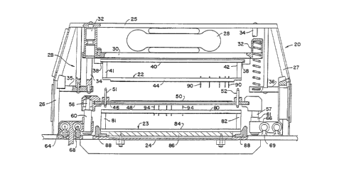
a test fixture of the present invention comprising
fxame assembly 20 with removable top or upper probe
module 22 and removable bottom or lower probe module
23 mountad thereon. Frame assembly 20 is provided
typically as a rectangular Prame having bottom wall
24, top wall 25 and side walls 26 and 27 to form
chamber 28 in which probe modules 22 and 23 are
releasably mountable~
As seating means for applying pressure to a
: lo circuit board under test, the embodiment shown
includes pneumatic bag 28 captured between top wall 25
and substantially planar, rigid pressure plate 30.
Plate 30 is secured at its edges to a plurality of
bushings 32 (preferably four, but only three being
shown) mounted on a plurality of vertical guide posts
34 (only three being shown) for linear motion along
the latter. Guide posts 33 and 34 are coupled between
top plate 25 and respeative ~upport arms 35 and 36,
each of the latter being connected to an intermediate
position along the interior o~ corresponding side
walls 26 and 27. Bushings 32 are spring loaded
between plate 30 and top wall 25 so that plate 30 is
resiliently biase~ toward top wall 25. Thus plate 30
is movable along a path constrained or defined by
posts 34 from an upper position at which plate 30 is
spaced from but is most closely adjacent top wall 25,
to a lower or extended position at which the travel o~
plate 30 brings bushings 32 into adjacency with
support arms 35 and 36.
As means ~or releasably mounting probe module 22
in normally spaced-apart relation to the circuit board
DMS-l
~3~3Z37
under test, the bottom surface of pressure plate 30 is
provided with a pair of horizontal channels or grooves
38 positioned respectively adjacent the side edges of
plate 30 so as to support the upper wall of top probe
module 22~ Probe module 22 is shown in the form of a
hollow hox having an upper wall 40, side walls 41 and
42, and bottom wall 44, upper wall 40 being
dimensioned to extend beyond the top edges of side
walls 41 and 42 so as to ~orm a pair of tongues 50
lo that in turn are dimensioned to fit slidingly but
snugly into grooves 38 located on the underside of
plate 30.
The embodiment o~ the invention shown in the
drawing also includes substantially planar,
board-support plate 46 ~or supporting boards to be
tested. Plate 46 includes a centrally disposed
aperture 48 therein, so that when a circuit board such
as board 50 is ~isposed on plate 46, access is freely
available to both sides of the board. Product support
plate 46 is preferably provided with guide means, for
example pins or the like pre-located in suitable
locations corresponding to pre-located holes in
cirauit board 50, so that when the circuit board is
properly mounted by engagement of such pins with the
corresponding holes, the locations o~ the test points
on the board will precisely correspond to or register
with the locations of the test probes in the probe
modules .
Mounted in fixed positions a~ the side edges of
plate 46 are at least two guide pins 50 and 51 that
extend perpendicularly both upwardly and downw.ardly
DMS-1
~3~)3Z3~7
--10--
from the plane of plate 46. Plate 46 is mounted
adjacent the corners thereof on four spring-loaded
plungers, only three of which, 56, 57 and 58, are
shown The plungers in turn are disposed for vertical
sliding movement within four respective cylinders 60,
51 and 62, the last not being shown.
In order to permit plate 46 to be moved in its own
plane from a first position wherein it is parallel to
and directly faces pressure plate 30 (and therefore
cannot be readily loaded with a circuit board~ to an
extended position in which it no longer faces plate 30
(and thus can readily ba loaded with a circuit board),
cylinders 60 and 62 are mounted upon glide 64, and
similarly, cylinder 61 and the fourth cylinder are
mounted upon glide 66. Glides 64 and 66 in turn are
mounted for linear, parallel sliding motion on
parallel rails 68 and 69 that are supported on bottom
wall 24. At least one of glides 64 and 66 is
connected through arm 70 to transmission belt 72. The
latter constitutes an endless belt extending between
idler whesl 74 and sheava 76 driven by reversible
motor 77.
Bottom probe module 23 is shown in the form of a
hollow box having an upper wall 80, side walls 81 and
82, and bottom wall 84, the module being dimensioned
to ~it between the undersurface of plate 46 and
support plate 86. The latter is resiliently mounted
on bottom wall 24. Frame 88 is also disposed on
bottom wall 24 to surround plate 86 and provide a snug
peripheral fit for modul~ 23.
Mounted on and extending perpendicularly
DMS-1
~3~3z3~
downwardly through bottom wall 44 of module 22 is an
array of a plurality of elongated, electrically
conductive test probes 90, all substantially parallel
to one another. The tips of probes 90 lie preferably
in a plane parallel to the plane of support plate 46.
The side edges of module 22 are provided with
respective bushings 91 and 92 disposed and dimensioned
to register with the upwardly projecting portions of
pins 50 and 52.
Mounted on and extending perpendicularly upwardly
through top wall 80 of module 23 is another array of a
plurality of elongated, electrically conductive test
probes 94, all substantially parallel to one another.
The tips o~ probes 9~ also lie preferably in a plane
parallel to the plane of plate 46. The side edges of
module 23 are provided with respective bushings 96 and
98 disposed and dimensioned to ragis~er with the
downwardly projecting portions of pins 50 and 52.
It will be appreaiated that the number o~ probes
extending from a particular probe module and the
pattern in which such probes may be arranged, are
dictated by the number and disposition of test points
on the circuit board to be contacted by the probes. In
this respect, it will also be appreciate~ that while
probe module 22 is intended to provide a probe array
for contacting the upper surface of a circuit board
under test and probe module -23 is intended to provide
probes for contacting test points on the underside of
the same board, the pattern and number of the arrays
o~ probes on the two module is not necessarily the
same and probably in most instances will differ
DMS-l
~L3~3237
-12-
markedly. The plurality of test probes 90 is thus
disposed in a ~ixed array determined by the location
of the test point.s on the upper sur~ace o~ the
specific type of circuit board 50 under test, and
similarly, the disposition in tha array of probes 94
is determined by the location of the test points on
the underneath surface o~ that particular type of
circuit ~oard 50.
Test probes 90 and 94 may be any of several
different types known in the art. The probes are
preferably of the spring-loaded type and should be
very hard, corrosion resistant and have partially
gold-plated tips. These features are desirable to
assure that each probe will be durable and will
provide low contact resistance. Spring-loaded test
probes with retractable tips are preferred because the
length is thus adjustable automatically to compensate
for irregularities in lavels among contact test
points. It is not uncommon ~or thousands of such test
probes to be required to te~t a circuit board.
Typically about four to about eight ounces of pressure
can be placed on each o~ the contact probes be~ore the
plunger is fully engaged.
Probes 90 and 94 are typically plugged into
receptacles having wire wrap posts at their bases in
the interior of respective probe modules. Each of
probes 90 is directly connected by a corresponding
conductor or wire 100 to a corresponding one of a
predetermined ~ixed number of connection points 102 in
the form of a plurality of electrical contacts such as
rivet heads or the like disposed in a ~ixed standard
DMS-l
~3~?3~:37
-13-
array. The array of connection points is mounted, for
example in bottom wall 44 of module 22 adjacent one
edge of the latter and are intended to interconnect
releasably with a corresponding plurality of probes
104 mounted on pedestal 106 fixed to wall 24 at the
bottom of chamber 28 in frame assembly 20. Probes 104
are the same in number as the number of connectio~
points 102 and are in an array matched to or mirroring
the array of connection points 104 so that every one
lo of pro~es 104 can simultaneously contact a
corresponding one of the connection points 102 in the
fixed standard array. Of course, the number of
connection points must at least equal and preferably
exceed the number of test points on the circuit board
under test, the excess number of connection points
simply being unused or blanked in each case.
For example, assume that the number of probes 90
in two ~ifferent modules 22 are respectively, as
dictated by the nature of the corresponding types of
circuit board~., 400 and 800. The number of connection
points 102 in each standard array on each of the two
different modules however is necessarily the same, and
one can further assume that each such array would
comprise 1024 suah connection points for example in a
rectangular 32x32 array. The replacement of one
module 22 ~or the other would provide exactly the same
number of connection points 102 although the number of
probes 90 required in the probe module would differ
markedly.
Similarly, each of probes 94 is directly connected
by a corresponding conductor or wire 108 to a.
DMS 1
~3~13;~7
-14-
corresponding one of a pred~etermined fixed number of
connection points llo disposed in a fixed standard
array in the foxm of a plurality of electrical
contacts such as rivet heads or the like. The latter
are mounted, for example in bottom wall 84 of module
23 adjacent one edge of the latter and are intended to
interconnect releasably with a corresponding plurality
of probes 112 mounted on bottom wall 24 of chamber 28
in frame assembly 20. Probes 112 are the same in
number as the number of connection points llo and are
in an array matched to the array o~ connection points
110 so that every one of probes 112 can simultaneously
: cont~ct a corresponding one of the connection points
110 in the fixed standard array.
It will be appreciated that the term "standard
array" as used herein is intended to indicate that the
number and physical location of connection points 102
and 110 and the corre~ponding array of probes 104 and
112 in a standard array with respect to each other are
established according to the wishes o~ the
manufacturer of the equipment and thus are arbitrary
and remain unchanged regardless of which particular
probe module is mounted in the frame assembly, whereas
the number and location of the array of probes 90 and
~4 of the probe modules are uniquely determined, not
by the manufacturer o~ the equipment, ~ut by the
configuration of contact or test points on the
speci~ic type o~ circuit board tv be tested This
identicality of connection point arrays permits the
substitution of an unlimited number of probe modules
in the system of the present invention, each for use
DMS-l
~3~3Z37
-15-
in testing circuit boards having different
configurations~
The standard arrays of probes 104 and 112 are
designed and intended to provide means for connecting
the probes in the probe modules through intermediate
connectors to a diagnostic device such as a computer
through output cables 114 and 116 respectively coupled
to probes 104 and 112. The use of such intermediate
connectors insures that the wiring between the probes
and the connection points is not flexed or otherwise
disturbed during operation of the system, and also
permits one to use the system with a huge variety of
probc arrays on different probe modules to test an
equally large number of circuit board configurations.
To test any particular circuit board 50 in the
~est fixture o~ the invention, one need only select
appropriate probe modules 22 and 23 which contain
respective probe array con~igurations mirroring the
test point configurat.ion on the opposite sides for the
specific type of circuit board 50 to be tested. The
probe modules aontain internally all the wiring needed
to conductively connect each o~ the probes in the
specific array patterns to the respective standardized
arrays of connection points 102 and 110. The
particular removable probe module 22 selected is then
inserted into the frame assembly chamber so as to
position module 22 within grooves 380 Similarly,
module 23 is positioned within frame 28.
Motor 78 is energized to drive belt 72 so as to
draw glides 6~ and 66 along rails 68 and 69 to an
extended position wherein support plate 46 is free of
DMS-l
~3~3;~:37
-16-
top probe module 22. Board SO is then emplaced on
plate 46 across aperture 48 so that the location of
test points on board 50 will exactly correspond to the
arrays of test probes 90 and 94. Motor 78 is then
reversed to move plate 46 and associated board 50 to
its proper position between the two probe modules. It
will be appreciated that the operation of motor 78 and
the loading of boards 50 on plake 46 can readily be
automated or computer controlled. Board 50 can be a
"loaded" board that supports electronic components
interconnected and mounted thereon in the
configuration intended for the ultimate use of the
board~ Of course, the invention is equally useful in
testing unloaded or so called "bare" boards. The
configuration o~ the components on the board is not
critical to the practice of the present inven~ion and
the invention is not intended to be limited to a
'^family" or single type of test board having a
particular number o~ test points arranged in a pattern
si.milar to one another.
Air under a positive pressure above atmospheric is
then introduaed into bag 28 to expand the latter and
apply pressure to plate 30. This serves to drive the
latter and top probe module downwardly along posts 34
against the spring loading of bushings 32 and causing
pins 50 and 52 to respectively engage bushings 91 and
92 to precisely align the top probe module with
product support plate 46. The continued downward
motion of module 22 ~rings the array of test points on
the upper surface of board 50 into physical and
electrical contact with the tips of the mirror-image
DMS 1
~3~3;~7
-17-
array of spring-loaded test probes 90,
aontemporaneously also bringiny contact points 102
into physical and electrical contact with the standard
array of intermediate connecting probes 104. These
two contacts thus eætablish and maintain a conductive
connection between those test points on the upper
surface of the board under test and the diagnostic
computer.
. Continued downward motion of the top probe module
; 10 drives probes so into the test points on board 50
against the resilient bias provided by the spring
loading in the array of probes so, ~orcing product
support plate 46 downwardly along plungers 56 against
the spring-loadin~ o~ cylinders 60. This downward
motion o~ plate 46 forces the lower portions of pins
50 and 52 into bushings 96 and 98, thereby precisely
aligning the bottom probe module with product support
plate 46. Continued downward motion of plate 46 under
the pressure exerted by the top probe module, brings
the test points on the lower surface of board 50,
exposed by aperture 48, into physical and electrical
contact with the mirror array of probes 94 and also
brings the standard array of connection points 110
into physical and electrical contact with intermediate
connection probes 112. These two con~acts thus
establish and maintain an electrically conductive
connection between`those test points on the lower
surface of the board under test and the diagnostic
computer.
Release o~ air pressure ~rom bag 2~ permits the
top and bottom probe modules to separate, under the
DMS-1
.
.
~l3~3~7
-18-
biases imposed by the resilient mounting of plate 86,
the spring-loadings in cylinders 60 and 61, and the
spring-lvading in bushing 32, from the board under
test and breaks all electrical connections in the
system between probes and connection points and probes
and test points. Plate 46 can then be extended again
by motor 78 and board 50 replace by a new board for
testing.
The variety of circuit boards which may be tested
in the test fixture of the invention is limited only
to circuit boards having a number of test points equal
to or less than the number of individual wires or
leads coupled between the standard arrays of probes
and the diagnostic computer.
Those skilled in the art will appreciate the
advantages of the arrangement just described. By
providing pre-wired modular units each having an array
of test probes which corresponds to the array of test
points in the type of circuit board being tested,
which modular units are readily detachable ~rom the
test fixture, a wide variety of circuit board layouts
can be quickly tested in a single test fixture without
the need for rewiring the test ~ixture for each type
of circuit board to be tested~
A cost savings over prior art circuit board test
equipment will result from implementation of the
present invention. This savings derives, in part,
from a savings in the cost of materials which must be
scrapped to adapt a new test fixture to a new circuit
board. Additional savings are derived from reduction
of down-time of the testing system, the lower ~apital
DMS-1
: ~L3~3;~37
-19-
outlay required for replaceable modules in lieu of
complete new test fixtures, and smaller storage
requirements for modules as compared to storage space
for many test fixtures.
It is to be understood that other changes may be
~`~ made without departing from the scope of the present
invention. Thus for instance, the assembly of the
present invention may be modified to accommodate only
one releasable probe module, so that only one side of
the board is tested at a time. It should be noted
that the frame may be directly wired to a diagnostic
computer, sr can be connected to a broadcast unit if
desired. The removable probe modules of the present
invention should not be considered limited to a box
form as described above, and indeed may assume a large
number of other configurations.
It is also contemplated that the seating means may
be any of the different types of means which have been
used for engaging the contact test probes with
different test points on a circuit board. These
include: (a) vacuum ~ixtures, in which the circuit
board is placed in a vacuum chamber which contains the
array of t.est probes so that the circuit board can be
forced under a vacuum against the array o~ test
probes; (b) mechanical pressure fixtures, in which a
mechanism is provided to engage an aligned circuit
board to be tested against the array of test probes
with sufficient force to establish and maintain a
positive electrical contact: and (c) other pneumatic
fixtures which are typically activated by pneumatic
bellows which create a pressure differential and cause
~,
DMS-1
~3~3;~
-20-
the circuit board to press against the array of
probes.
The test fixture of the present invention is
characterized by simplicity of construction,
flexibility, ease of assembly and disassembly and
overall convenience of use. It promotes precision
high speed testing of a wide variety of circuit
boards, regardless of the configurations of the
components mounted thereon. Its many improvement
features should now be apparent.
Even though the advantages have been set forth in
the foregoing description, together with the details
of the structure and function of ~he invention, it is
to be understood that the disclosure is illustrative
only. Various changes in shape, size and arrangement
of parts may be resorted to without departing from the
scope of the invention which is indicated by the broad
general meaning o~ the terms in which the appended
claims are expressed.
DMS-1