Note: Descriptions are shown in the official language in which they were submitted.
~303253
- 1 -
PROCESSES DEPENDING ON PLASMA GENERATION
Back~round of the Invention
1. Field oP the Invention
This invention, relates to plasma processing and in particular to plasma
5 processing of devices.
2. Description o~ the Pr or Art
Plasma discharges are extensively utilized in the fabrication of devices
such as semiconductor devices and, in particular, silicon semiconductor devices. For
example, plasma discharges in appropriate precursor gases are utilized tO induce10 formation of a solid on a deposition substrate. (One important embodiment of such a
procedure is called plasma assisted chemical vapor deposition.) In a second plasma
dependent procedure, species generated in a plasma are utilized to etch a substrate,
e.g. a device substrate being processed which generally includes dielectric material,
semiconductor material andlor material with metallic conductivity.
In plasma-assisted deposition procedures the desired solid is comrnonly
formed by the reaction of a gas composition in a discharge. In one variation,
reactive radical(s) formed in the plasma region either alone, or as rnixed outside of
the discharge region with a second gas, are flowed over a deposition substrate remote
from the discharge to form the desired solid film. In another variation, the substrate
20 is surrolmded by a plasma which supplies charged species for energetic ion
bombardment. The plasma tends to aid in rearranging and stabilizing the film
provided the bombardment is not sufficiently energetic to damage the underlying
substrate or the growing film.
In etching procedures, a pattern is typically etched into the substrate by
25 utilizing a mask having openings corresponding to this pattern. This mask is usually
formed by deposi~ng a polymeric photosensitive layer, exposing the layer with
suitable radiation to change the solubility of the exposed regions, and then utilizing
the induced change in solubility to form the desired pattern through a solvationprocess.
For most present day device applications, it is desirable to produce
anisotropic etching at an acceptable etch rate. (Acceptable etch rates depend upon
the material to be removed and are generally those that remove at least 2% of ~elayer thickness in a minute. Anisotropic etching for the purpose of this descripdon is
an etch which undercuts the etch mask a distance less than one ~quarter the layer
35 thickness.) The production of relatively vertical sidewalls duling anisotropic etching
allows higher packing densi~ies for device structures. Additionally, the producdon
~3~3253
- 2 -
of a relatively high etching rate leads to shorter processing times.
In one method of anisotropic etching, appropriate charged species
generated in the plasma produce energetic ion bombardment that induces aniso~ropic
etching. Various sources for producing the desired plasma discharge have been
S employed. For example, parallel plate reactors as described in C. J. Mogab, VLSI
Technolo~y, ed Sze at McGraw-Hill, NY 1983, lpgs. 303-345, and reactors having
hexagonal electrodes as described in U.S. Patent 4,298,443 dated November 3, 1981
have been employed to induce aniso~opic etching. Radio frequency resonators suchas helical resonators have been used at pressures above 0.1 Torr as a source of
10 etching species solely for isotropic etching. The species generated in the resonator
are chemically reactive but have not demonstrated d~e momentum required for
anisotropic etching.
As an alternative, a technique based on electron-cyclotron resonance
(commonly referred to as ECR) discharges that generate high energy species for
15 anisotropic etching has been described for the generadon of ions at low pressure.
(See Suzuki, et al. Journal of the Elec~ochemical Societx 126, 1024 (1979).)
However, the relatively high cost of an ECR is not entirely desirable. Additionally
the etching of device structures suitable for 0.25 ~Lm devices has not been reported.
Summary of the Invention
It has been found that not only is electron-cyclotron resonant etching
extremely expensive but also that this etching procedure under many circumstances
produces rapid heating of the substrate being etched and degrades ex~emely fine
etching pattems. It has fur~her been found that the use of a helical resonator
operating at pressures below 10 mTorr produces sufficiently energetic species to25 result in downstream anisotropic etching without any substantial heating of the
substrate being etched. Additionally the low pressure yields etch rates faster than
500 A/min.
Indeed, a helical resonator operating at low pressure is, in general, an
excellent source of charged species for procedures such as ion implantation, surface
30 modificadon, and downstream reaction to induce deposition. A helical resonator is
also an excellent source of reactive radicals for inducing deposition, etching, surface
cleaning, and surface modification such as a hydrogen atom source, e.g. for
molecular or chemical beam epitaxy.
~3~3~53
In aceordance with one aspect of the invention there is provided a process
for fabrieating a device eomprising the steps of subjecting a substrate to a composition
entities that induce anisotropic removal of material from said substrate and employing the
resulting substrate for eompletion of said deviee, characterized in that said entity
S emanates from a species generated in a helical resonator wherein said species is from a
discharge in a gas at a pressure less than about 10 mTorr.
In aeeordance with another aspect of the invention there is provided a
proeess for fabricating a device comprising the steps of subjecting a substrate to a
composition comprising entities that induce deposition on said substrate and employ the
10 resulting substrate for completion of said device, eharaeterized in that said entity
emanates ~rom a speeies generated in a helical resonator wherein said substrate is within
said resonator.
.. ..
~'~'. .
13032~3
- 3 -
Brief Description of the Drawin~
FIGS 1-S are illustrative of apparatuses suitable for practicing the
invention.
Detailed Descripti
As discussed, the invention relies on the use of a helical resonator to
produce a plasma in a gas at low pressure, i.e. a gas at a pressure of less than 10
mTorr for processes such as etching procedures or implantatdon procedures.
Alternatively, a helical resonator is used to maintam a plasma in a precursor gas
typically having a pressure in the range 10-5 to 100 torr for generation of species to
10 be employed in procedures such as deposition. For pedagogic purposes, use of the
helical resonator will be described in terms of the etching procedure. Condi~ons that
differ for other uses of the generated species will subsequently be discussed.
Design of helical resonators are generally discussed in W. W.
MacAlpine et al, Proc. of IRE, page 2099 (l9S9) and generation of a plasma w-th
15 these resonators is described in C. W. Haldeman et al, Air Force Research LabTechnical Research Report, 69-0148 accession No. TL501.M41, A25 No. 1~6.
(Although optimum resonance conditions are described by MacAlpine, for the
procedures of this invendon conditions substantially deviating from optimal are
useful and, in fact, allow use of larger resonators. For example, a radius of the spiral
~0 coil more than 0.6 times the radius of the shield is quite useful.) The helical
resonator includes an outside enclosure of an electrically conductive material, e.g. a
cylinder, an internal helical coil of an electrically conductive material, if desired, an
applied magnetic field in an axial direction in the region enclosed by the coil to
enhance electron confinement, and means for applying an rf field to the coil.
25 Typically, the outside enclosure and helical coil is of an electrically conductive
material such as copper.
It is possible to operate the helical resonator either in a half wave rnode
or a quarter wave mode. It is possible in the half wave mode to connect both ends of
ehe helical coil to the outer shield so that the resonator coil is grounded at bo~ ends
30 to allow the electrical matching tap or coupling to be located toward either end. In
the quarter wave mode it is possible to connect one end of the coil to the outer shield
and to insulate and separate the opposite end from the shield to reduce capacitance
coupling. Useful processing is perfolmed by positioning the floaeing end of the coil
in a quarter wavelengeh configuration at ei~her end.
~3(:1 3253
The plasma discharge is contained within a low loss dielectric,
- insulating enclosure (e.g., a quartz tube) that passes through and is preferably
concentric with the inner coil of the resonator. It is possible to use gas enclosure
materials with higher loss or with both higher loss and higher dielectric constant.
S However, the former lowers the resonant "Q" of the circuit and the latta leads to not
only lower "Q", but also lower resonant frequency. The enclosure dimensions
should be consistent with the diameter of the helical coil and are sized tO provide a
relatively uniform plasma flux at the substrate that, in ~n, provides a concomitantly
uniform deposition or etching. (A control sample is easily employed to determinelû suitable dimensions for a desired flux.) Precursor gases are flowed into the
enclosure, pass through the discharge and exit.
The magnetic field utilized in the region of the coil, if desired, in
conjunction with the helical resonator should generally be greater than 50 Gauss as
measured at the axis of the helical coil. Fields weaker than 50 Gauss do not produce
15 substantial plasma enhancement. The frequency of the appliecl rf power is notcritical but does affect the resulting etching. Generally, frequencies above 80 MHz
lead to impractically small resonator sizes and frequencies below 3 MHz lead to
plasma instabilities and excessive physical dimensions. (It is also possible to use a
combination of frequenc;es during etching if they are resonant harrnonics of each
20 other. Resonant harmonics, however, are generally not exact multiples and a
suitable frequency is obtained by tuning until a plasrna together with a low standing
wave ratio at the electrical transmission line are obtained.) Typically a power
density generally in the range 0.05 Watts/cm3 to 1 Watts/cm3 of discharge volume is
employed. Power densities below 0.05 Watts/cm3 yield low specific ion fluxes and25 power densities above 1 Watts/cm3 lead to excessive heating of the discharge
enclosure. (Discharge volurne is defined here as the volume of dielectric discharge
tube enclosed by the resonator coil.)
Generally the larger the outer enclosure, the internal coil and ~e
dielectric discharge tube, the greater the integral flux of the species pr~duced.
30 Typically, resonator cavities having coil diameters in the range 2.5 cm to 60 cm are
utilized. Cavities smaller than 2.5 cm in diarneter are less desirable because of the
relatively low integral flux of ions and cavities larger tha n 60 cm, although not
precluded, are inconvenient because of the mechanical size, the lowered resonantfr~uency, and the increased power required. The cavity is brought to a resonant
35 condition by adding capacitance to the coil, adjusting the length of the coil or
adjusting the rf frequency to resonance. (It is possible to extend the resonance length
~3~3; :~.3
of a coil by increments of approximately the wavelength divided by two, e.g.
2 ~ l, 3, 2 of the wavelength, etc. for halfwave resonators and 4, 4, 4 of the
wavelength, etc. for quarter wave resonators, while maintaining the same discharge
mode. This relationship is not precise because in practice, plasma loading effects
5 and fringe capacitance influence the resonant frequency. Nevertheless, the
relationship allows deterrnination of a suitable range with precise values for adesired set of conditions determined with a control sample.) Cooling means such as
circulating fluid through the coil or passing cooling gases through the resonator
assembly are possible.
As discussed, it is advantageous to ground one end of the helical coil,
and pre~erably when used in a half wave or multiple mode device both ends are
advantageously grounded. (Grounding, although not essential to its operation, tends
to s~abilize the plasma operating characteristics. Additionally, grounding on both
ends reduces the possibility of coupling stray current to nearby metallic objects.)
15 Standard means are employed to couple rf power to the resonator. For example, a
tap on the coil is made at a point where the voltage to current ratio is approximately
equal to the characteristic impedance of the rf source at operation. Alternatively, it
is possible to use a coupling loop.
It is possible to position longitudinally conducting elements along the
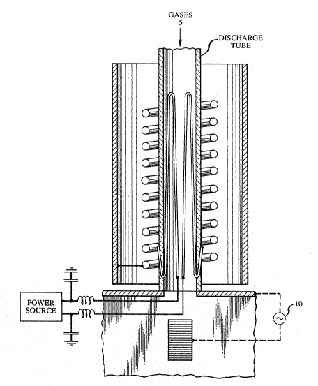
20 outside of the low loss dielectric discharge tube. For example, a heater as shown in
FIG. 1 or a split metallic shield as shown in FIG. 2 are advantageously employed for
many applications. The heater, in particular embodiments, is useful in deposition
procedures to heat the deposition substrate when the substrate is positioned within
the discharge tube or to heat species generated in the plasma ~or subsequent
25 downstream etching or deposition. The shield, in particular embodirnents, is useful
to adjust plasma species concentrations by applicadon of a bias or to shield theplasma region from radial electric fields. If the longitudinal conductor is employed it
should not form a low impedance, conducting loop in the circumferential direction.
Thus the shield is shown split in FIG. 2 and the heater although seTpentine does not,
30 as shown in ~IG. 1, complete a loop within the resonator coil. (It is possible to
complete the loop outside the conducting coil since the impedance of this completed
portion is quite high.)
Gases for etching are introduced in the region of the helical electrode at
a pressure in the range, lxlO-s Torr to lO mTorr. Unexpectedly, relative1y low
35 pressures sustain a plasma and yield an intense flux of ions. Indeed, press~ll es above
~3~3Z53
- 6-
10 mTorr are not desired for etching since the relative flux of ionic species that
induce anisotropic etching in proportion to neutral species -- neutral species tend to
cause isotropic etching in the absence of sufficient ion flux -- is substantially lower.
Pressures below lx10-5 Torr although not precluded are also not desirable since the
5 plasma becomes difficult to initiate and operate.
The gas employed depends upon the material to be etched. A wide
vanety of gases have been udlized to etch the materials typically employed in
devices such as semiconductor devices. For a review of suitable etchants, for
numerous material utilized in devices see D. L. Flamm et al, 5ILSI lec onics:
10 Microstr cture Science, Vol. 8, N. ~3. Einspruch and D. M. Brown, eds, Academic
Press, New York9 1984, Chapter 8. Exemplary of such gases are chlorine, utilized to
selectively etch silicon over SiO2, and NF3 for selective etching of SiO2 over GaAs.
The etching gases are advantageously introduced at nne end of the resonator tubesuch as shown at S in FIG 1. It is possible tO use the etchant gas itself at a suitable
15 pressure or to mix the etchant with other gases such as an inert gas, e.g. argon.
Irrespective of the particular gas or combination of gases utilized the pressure should
still be maintained below 10 mTorr.
A typical configuration for downstream etching is shown in nG 3. The
distance between the discharge and substrate depends on 1) coupling between the
20 discharge and the etching chamber 2) the relative areas of the discharge tube cross
section and the etching chamber, 3) gas pressure and 4) any additional bias
employed. However, typically tbe substrate is placed a distance of at least 0.5 the
diameter of the dielectric gas enclosure from the plasma. (For purpose of this
disclosure, bias refers to a d.c. or a.c. electrical potential applied between a25 reference surface, e~g. the resonator shield or independent electrode, and the
substrate.)
For etching anisotropically in a direction perpendicular to the surface, it
is generally desirable for the major surface of the substrate to be positioned
perpendicular to the direction of the ions emanating fiom the plasma. It is possible to
30 bias the substrate (10 in FIGS 1 and 3) and if desired, to pulse this bias and/or pulse
the discharge itself. Pulse rates in the range 0.1 Hz to 150 kHz are useful. Pulsing
of the bias is of particular use when a multilevel resist is employed with a silicon
containing top level and a planarizing lower level. The use of a pulsed bias with
oxygen etching species alternates etching of the underlying resist with formation of
35 an etch resistant silic~n dioxide layer on the pattemed overlying resist. Thus, the
pattern is transferred into the underlying resist with substantially no degradation of
~3032S3
the overlying pattern dunng ~his transfer.
Pulsing of the discharge is advantageous, for example, when multiple
plasma sources or feed gas flows are employed. With suitable pulsing the source of
etching species (or deposition species in deposition processes) are controlled by a
S time variation in power applied to different etchant sources, e.g. completely
different resonators, one resonator with a time variation in gas flow composition or
other sources of chemical reactants which may optionally be partially dissociated by
an additional plasma device. (Pulsing of the discharge dunng a deposition process
also leads to increased deposition rate under approp~iate conditions.)
lû The inventive process has been found particularly suitable for etching of
devices based Otl extremely strict design rules, for example, a device based on 0.25
~,lm long gate structures of ~ansistors. Dimensions ~is small generally are not
adequately etched by available techniques. Nevertheless, by using a helical resonator
at low pressure, extremely good resolution at an acceptable etch rate is obtained. For
15 example, the etching of polysilicon using a chlorine discharge generated by helical
resonator at a pressure of 10~ Torr yields well resolved 0.25 ~m structures
separated by 0.25 ,um spaces. Addidonally, this structure is produced at an etching
rate of approximately 200 A/min. Thus even for extremely fine structures,
anisotropic, well resolved etching is produced.
The parameters employed for species generation for other uses suçh as
ion implantation, surface modification or multiport processing (such as a source of H
atoms, or ~ for molecular beam epitaxy), and downstream deposition based on the
use of a helical resonator are similar to those utilized for etching. Pressures in the
range 1~5 to 100 Torr are suitable for a variety of applications and the precise25 pressure for a given situation is determined with a control sample. The gasesudlized for deposition depends on the species desired. A wide variety of gas
precursors are well known for producing particular deposited material. Exemplaryof sui~able precursors are an 2 plasma for subsequent reaction with
tetraethoxysilane to deposit SiO2.
Additionally, it is possible to enhance the deposition discharge by
introducing an axial magnetic field in the discharge region, as in the case of etching
(e.g. 20 in FIG 3). Moreover, it is possible to further control the deposition or
etching process by introducing electric and magnetic fields near the substrate region
(shown in phantom at 21 and 22 in FIG 3). It is possible to employ fields that are
35 purely axial, purely radial, or a supeIposition of axial and radial ~i~lds with respect tO
the resonator axis.
13~)3~53
- 8 -
These fields are useful as shutters, as a means to direct the ions to a
particular position on the substrate, as a means to alter the radial distribution of the
plasma stream across the substrate diameter, or as a means to regulate impact energy.
It is also possible to impose an RF electric field onto the substrate tO further control
S ion bombardment energy during deposition or etching. llle conditions of this
particular mode of operation are fixed so that no discharge, or only a very weakdischarge, is sustained by the 3~F potential unless the resonator plasma is on, i.e., a
nonself-sustaining discharge is forrned. In this instance the helical resonator
discharge acts as a virtual electrode. Most significantly, deposition in the discharge
10 region as shown in FM 4 is possible. As in etching and othe~ deposition processes,
use of a heater, 41, around substrates 42 held in a horizontal position or as shown in
phantom at 43 held in a vertical position is suitable if desired. Additionally, as in
other embodiments a bias, 44, to the substrate support is acceptable.
EXAMPLE 1
A 350 A layer of SiO2 was grown by the procedure described in L. E.
Katz, VLSI Technol~y ed. Sze at McGraw Hill, NY, 1988, pgs. 98-140, on a
100 mm diameter silicon wafer with the major wafer surface oriented in the (100)
plane. A 3000 A film of undoped polycrystalline silicon was deposited by chemical
vapor deposition (as described in A. C. Adams, VLSI Technolo~y ed. Sze at
20 McGraw-Hill, NY, 1988, pgs. 238-248), onto the silicon dioxide. An etch mask
having 0.25 ~lm lines and varying spaces was formed by a txilevel patterning scheme,
as described in "Electronic and Photonic Applications of Polymers", M. J. Bowdenand S. R. Turner, eds., pp. 90-108, (American Chemical Society, Washington, D.C.),
1988. The trilevel resist included a first layer (4500 A) of a planarizing Novalac
25 polymer, an overlying 1200 A thick plasma deposited SiO2 layer and a top layer of
an electron beam sensitive resist (chlorinated glycidyl methacrylate). The top layer
was exposed to an electron beam writing apparatus producing 0.25 ~m features. This
pattern was transferred through the oxide layer by reactive ion etching, and theunderlying layer of planarizing polymer was etched with oxygen reactive ion etching
30 to complete the pattern transfer to the polycrystalline silicon.
The entire wafer was transfelred into an etching apparatus shown in PIG
S via a vacuum loadlock 51, using motor drives 52 and 53 as well as wafer cassette,
54. The subs~ate 59 was held on a plate insulated from ground that could be biased
13~i3253
with a separate 13.56 MHz rf source. A helium-neon laser, was used to monitor the
polysilicon etch rate by laser interferometry. The reaction chamber was evacuated to
a pressure of sx10-7 torr with a diffusion pump, backed by a Roots blower and
mechanical pump. A quarter wave helical resonator was employed to sustain a
5 plasma that coupled during etching to an underlying aluminum reaction charnber.
The resonator, 60, was constructed from a 12 in. Iong, 8 in. O.D. cylindrical copper
shield containing a 27 turn, 6.5 in. long, helical coil, 61, of 1/8 in. O.D. copper
tubing, 4.5 in. O.D.. The fundamental resonance of this structure (approximately8.7 MHz) varied slightly with the applied RF power and gas pressure. A
10 64 mm O.D. qua~z discharge tube, 63, t498 cm3 discharge volume within the coil)
passed concentrically through the helical coil, was mated to the reaction chamber,
64, by o-ring seals, and extended 2 in. into the chamber. The end of the discharge
tube was positioned approxirnately 6 in. ~rom the substrate. Gases were passed
through the opposite end of the tube which extended 10 in. beyond the resonator
15 shield. The resonator was placed close to the top metal flange of the reaction
chamber. A flow of air was passed through the resonator to cool the quartz tube.Chlorine was flowed through the quartz discharge tube at 15 sccm
yielding a pressure of approximately 10~ torr within the reaction chamber. ~It is
possible to use small additions, e.g. 1 to 15% of oxygen to the discharge to increase
20 the polysilicon to silicon oxide etch rate selectivity.) A discharge was initiated by 1)
coupling an RF amplifier and frequency generator to the resonator coil, tuning the
sine wave frequency near resonance as indicated by a sharp decrease in the voltage
standing wave ratio at the input to the resonator and the appearance of a visible glow,
and 2) increasing the applied yower to a level of approximately 80 W. Adjustment of
25 frequency and power were normally performed in concert. Power inputs to the
resonator circuit were approximately 75 W, (0.15 W/cm3 power density into the
volume of the dielectric tube enclosed by the helical coil) yielding an etch rate in
undoped polysilicon of 200 A/min. (Increasing the power increased dle polysilicon
etch rate. Higher powers were usable but the discharge glow in the charnb~r became
30 somewhat unstable.) Etching was continued 1.6 times the period required to remove
the exposed 3000 A layer of polysilicon in the center of the wafer as measured by the
laser interferome~y. The discharge and gas flows were then extinguished and the
wafer was removed for analysis~
~l3032S3
- 10-
With either Cl2 or Cl2/02 discharge mixtures, the etch selectivities for
polysilicon over oxide and the resist were acceptable, but the selectivities were 'oetter
with oxygen additions. Polysilicon/oxide selectivity was approximately 30:1 withCl2 and 70:1 with Cl2/O2, while the polysilicon/resist selectivity was -2.5:1 in both
5 cases. Scanning electron micrographs of the masked regions showed smooth, nearly
vertical sidewalls for the polysilicon with no undercutting.
EXAMPLE 2
The same configuration as that described in Example 1 was used except
that the substrate was cooled below ambient temperature. This was accomplished by
10 flowing cold fluid through the substrate platen and subsequendy cooling the wafer to
be etched by conduction. Temperature was regulated by adjusting the fluid flow or
fluid temperature, or providing an additional heating source. Temperatures in the
range -180 to 201: were employed. Etching of the substrate was performed as in
Example 1. In tnis case the etch selectivities for polysilicon over gate oxide and the
15 resist were increased compared to those given in Example 1. Lower substrate
temperature ~avored etching material with a lower activation-energy to reaction7 e.g.
polysilicon.
EXAMPLE 3
A similar configuration to that descri'oed in Example 1 was used to
20 deposit silicon dioxide films. A portion of an undoped (100) silicon wafer was used
as the deposition substrate. The helical resonator employed has a primary resonance
of 18 MHz. The resonator excited a diseharge in 2 (100 sccm at 0.2 Torr) which
passed through a quartz tube that was 1.4 in. O.D. The discharge tube was coupled
to a quartz reactor having a heated substrate holder (430C). Tetraethoxysilane was
25 introduced downstream of the discharge at a rate of 5 sccm in the region above the
substrate. One hundred watts of power was applied to the resonator yielding a
deposition rate of 600 A/min.
The resulting films were analyzed by fourier transform infrared
spectroscopy and Rutherford backscattering spectroscopy. The analysis of the films
30 showed essentially pure silicon dioxide. Oxide filrns deposited at 25C had asignificant concentration of OH groups and a somewhat decreased film density.
However, the film composition and density were improved by using a 200 kHz RF
bias (900 V peak-to-peakj on the substrate holder, to enhance ion bombardment
rearrangement and stabilization of the film. The additional RF bias did not affect the
i3032S~
discharge cu~rent flowing from the resonator plasma.
EXAMPLE 4
A hotwall, quartz discharge tube 70 cm long and 50 mm O.D. was
passed through a resonator centered at 8.7 MHz. The tube was heated by a
S cylindrical furnace slightly smaller than the resonator coil and thermally insulated
from the resonator volume having the heater elemen~ in a serpentine array so that
continuity was avoided around the circumference of the heater. The heating element
when mounted in this fashion did not hinder the operation of the discharge. The tube
was heated tO approximately 500C and air cooling kept the resonator components
10 from heating excessively. Both ends of the helical coil were electrically referenced
to the shield, i.e. the resonator was operated in a half wave mode and the second
harmonic (approximately 18 MHz) was used.
Fluorinated silicon nitride was plasma deposited by introducing a
200 sccm flow of 1% silane in helium and a 4 sccm NF3 flow directly on the silicon
15 wafers held in the resonator discharge. Pressure in the discharge was maintained at 1
torr, the quartz wall was maintained at 350C and the power was 50 W. The
resulting deposition rate was 200 A/min. Analysis of the film showed nitrogen,
fluorine and silicon.
~3~:)3253
EXAMPLE S
The procedure of Example 3 was followed except the deposition rate
was enhanced by turning the resonator discharge on and off with a duty cycle of
50%. This modulation of the discharge was performed in the frequency range 0.1 Hz
S to 20 kHz. The effect was related to fonning a discharge with unreacted feed gas in
the wafer region and turning the discharge off to allow more undepleted feed gas to
enter the region. Enhancement in the deposition rate was approximately a factor of
two over the continuous discharge mode, depending upon the modulation period.