Language selection

Search

Patent 1303382 Summary

Third-party information liability

Some of the information on this Web page has been provided by external sources. The Government of Canada is not responsible for the accuracy, reliability or currency of the information supplied by external sources. Users wishing to rely upon this information should consult directly with the source of the information. Content provided by external sources is not subject to official languages, privacy and accessibility requirements.

Claims and Abstract availability

Any discrepancies in the text and image of the Claims and Abstract are due to differing posting times. Text of the Claims and Abstract are posted:

  • At the time the application is open to public inspection;
  • At the time of issue of the patent (grant).
(12) Patent: (11) CA 1303382
(21) Application Number: 1303382
(54) English Title: OPTICAL DETECTOR STORAGE EFFECTS REDUCTION
(54) French Title: REDUCTION DU STOCKAGE DES SIGNAUX D'UN DETECTEUR OPTIQUE
Status: Expired and beyond the Period of Reversal
Bibliographic Data
(51) International Patent Classification (IPC):
  • G01B 11/00 (2006.01)
  • G01D 05/26 (2006.01)
  • G01D 05/34 (2006.01)
(72) Inventors :
  • BRAND, DONALD L. (United States of America)
(73) Owners :
  • TEKTRONIX, INC.
(71) Applicants :
  • TEKTRONIX, INC. (United States of America)
(74) Agent: KIRBY EADES GALE BAKER
(74) Associate agent:
(45) Issued: 1992-06-16
(22) Filed Date: 1987-10-27
Availability of licence: N/A
Dedicated to the Public: N/A
(25) Language of filing: English

Patent Cooperation Treaty (PCT): No

(30) Application Priority Data:
Application No. Country/Territory Date
931,491 (United States of America) 1986-11-17

Abstracts

English Abstract


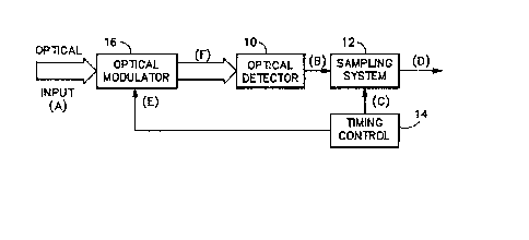
Abstract of the Disclosure
Optical detector storage effects reduction is
achieved by inserting an optical modulator between the
optical signal to be measured and the optical
detector. The modulator is normally turned off, and
is only turned on during the period when the output of
the optical detector is being sampled by a sampling
system.


Claims

Note: Claims are shown in the official language in which they were submitted.


- 5 -
WHAT IS CLAIMED IS:
1. An improved optical measurement system of the type
having an optical detector to which an optical signal
to be measured is input, the output of the optical
detector being sampled by a sampling system, wherein
the improvement comprises means for inhibiting the
input of an optical signal to the optical detector
except during the time when the output of the optical
detector is being sampled by the sampling system.
2. An improved optical measurement system as recited
in claim 1 wherein the inhibiting means comprises.
an optical modulator having the optical signal as
an input and outputting a modulated optical signal for
input to the optical detector; and
means for turning on the optical modulator only
during the time when the output of the optical
detector is being sampled by the sampling system.
3 . An improved optical measurement system as recited
in claim 2 wherein the turning on means comprises a
timing control circuit which generates a sample strobe
for the sampling system to sample the output of the
optical detector and a modulator strobe for turning on
the optical modulator, the modulator strobe being
approximately concurrent with the samples strobe and
having a pulse width greater than or equal to that of
the sample strobe.
4. An improved optical measurement system as recited
in claim 3 wherein the timing control circuit outputs
a plurality of sample and modulator strobes at a rate
determined by the storage effects decay time of the
optical detector such that samples are obtained in the
absence of the storage effects.

Description

Note: Descriptions are shown in the official language in which they were submitted.


~ ~3~D33~2
OPTICA~ DETECTOR ~TORAGE EFFECT5 REDUCTION
ackqround of the Invention
The present invention relat~s to optical
detectors, and more particularly to a method for
reducing the optical detector Rtorage ef~ects o~ a
high speed optical measuring 8y8tem.
High speed optical ~ignal~ are csmmonly mea~ured
by applying the signal continuously to an optical
detector and 6ampling the detector output signAl with
an electronic 6ampling ~ystem. ~ch a yste~ i~ used
in the OF150 Serie~ of Fiber optic Ti~e Domain
R~flectometer~ manu~actured by Tektronixt ~nc. of
Beavarton, Oregon. Assuming a pul~ed input, the
output of the detector at the tra~ling edge o~ ths
input pulse i~ in the ~orm of an exponent~al decay due
to the 6torage ti~e o~ the deteotor. A ~ample ~tro~
applied to the ~ampling ystem ~ro~ a timing control
during the decay portion of the detector output wiIl
re~ult in a sample output whioh has a ~igni~icAnt
srror ~rom the actual value o~ th~ ~nput pul~e. What
iS deBired i6 a method ~or reducing the e~fects o~ the
6torage time o~ the deteotor to produce ~ more
accurate value at the output.

~3~8~
, . . .
Sulrunary of the ;I:nvention
Accordingly the presant invention provide~ an
optical detector storage effects reduction method by
using an opt~cal modulator device to reflne and
improve the performance of the optical d~t~atorO An
input optical signal is input to the optical modulator
which is turned off prior to the ~ample tlme,
preventing light from reaching the optical det2ctor.
The modulator iB then turned on ~ust before or
concurrent with the beginning of a sample strobe.
Thus the optical signal iB prevented from reac~ing the
detector and creating storag~ e~fects that may distort
the electrical output signal during the 6ampling timeA
The ob~ects, advantages and other novel features
of ths present invention are apparent from the
following ~etailed description when read in
conjunction with the appended claims and attached
drawing.
Brief Description o~ the Drawing
Fig. lA is a block d-iagram of a prior art optical
measurement system.
~ ig. lB ls a timing diagram ~or the prior axt
optical measurement sy6tem o~ Fig. lA.
Fig. 2A is a block diagram of a high speed optical
measurement ystem according to the present inventionO
Fig. 2B is a timing diagram for the optical
~easurement ~ystem o~ Fig. 2B~
bescript~on of the Preferred_Embodiment
Referring now to ~ig~. lA and ~B a prior art

~3~ 3~32
optical measurement ~ystem has an optlcal detector 10
to which i~ input an optical signal, indicated by
(A). The output of the optical detector, i~dicated by
(B), is input to a ~ampling 8~8te~ 12. Tha ~ampling
6ystem 12 6amples the output of the optical detector
when triggered by a ~trobe pulse, indicated by (c),
from a timing control circuit 14. The resultiny
output from the -ampling system 12 is indicated by
(D), showing that there is an error in the mea~urement
value as opposed to the actual value o~ the optical
signal at the sampl$ng time.
Fig~. 2A and ~B 6how an optical measurement 8y6tem
having an optical modulator 16 inserted prior to the
optical detector 10. The output of the optical
modulator 16, indicated by (F), i~ then input to the
optical detector 10, the output of which 1~ sampled by
the sampl ing 6ystem 14 as in the prior art. The
optical ~odulator 16 is turned o~f pr$or to the 6ample
strobe from the timing control circuit 14. ~ust prior
to, or concurrent with, the generation o~ the sample
strobe from th timing control circuit 14, the timing
control circuit 14 applies a modulator ~trob~ pulse,
as indicated by (E), to the optical modulator 16 to
turn on the modulator and pass a port~on (F~ o~ the
optical signal (A) to the optical detector 10. The
~ample ~trobe ~C) sample~ the optical detec~or ou~put
tB) to produce the sample output (D) which now
represents the actual valu~ of the optical input (A)
at the sample time.
For multipls samples the interval between ample~,
~.e., between optical modulator turn on t~mes, is
determined by the time required to allow the fitorage
e~ects of the optical detector 10 to decay. ~l~o the
turn on ti~e o~ the optical modulator is kept as ~ort

~" ~L3~3~2
as possible, i. 2., the turn on time i6 only as long as
the ~ampling 6y6tem 12 requires to obtain the 6ample.
Therefore lf the etorage ef~ects decay time for the
~aximum valua of the opt~cal input signal 18 lOO
nsecs, then the optical ~ignal may be sampled at a 10
MHz rate.
Thus, the present invent$on provides a ~eans ~or
improving the performance of high 6peed optical
measurement systems by decreasing the e~ects o~
optical de~ector storage time through the use of an
optical modulator at the lnput of the optical
detector, the optical modulator bsing turned on only
during the sample time,

Representative Drawing
A single figure which represents the drawing illustrating the invention.
Administrative Status

2024-08-01:As part of the Next Generation Patents (NGP) transition, the Canadian Patents Database (CPD) now contains a more detailed Event History, which replicates the Event Log of our new back-office solution.

Please note that "Inactive:" events refers to events no longer in use in our new back-office solution.

For a clearer understanding of the status of the application/patent presented on this page, the site Disclaimer , as well as the definitions for Patent , Event History , Maintenance Fee  and Payment History  should be consulted.

Event History

Description Date
Inactive: IPC from MCD 2006-03-11
Inactive: Adhoc Request Documented 1996-06-16
Time Limit for Reversal Expired 1995-12-17
Letter Sent 1995-06-16
Grant by Issuance 1992-06-16

Abandonment History

There is no abandonment history.

Owners on Record

Note: Records showing the ownership history in alphabetical order.

Current Owners on Record
TEKTRONIX, INC.
Past Owners on Record
DONALD L. BRAND
Past Owners that do not appear in the "Owners on Record" listing will appear in other documentation within the application.
Documents

To view selected files, please enter reCAPTCHA code :


To view images, click a link in the Document Description column. To download the documents, select one or more checkboxes in the first column and then click the "Download Selected in PDF format (Zip Archive)" or the "Download Selected as Single PDF" button.

List of published and non-published patent-specific documents on the CPD .

If you have any difficulty accessing content, you can call the Client Service Centre at 1-866-997-1936 or send them an e-mail at CIPO Client Service Centre.


Document
Description 
Date
(yyyy-mm-dd) 
Number of pages   Size of Image (KB) 
Abstract 1993-10-31 1 11
Claims 1993-10-31 1 46
Drawings 1993-10-31 2 32
Descriptions 1993-10-31 4 133
Representative drawing 2002-04-21 1 6
Maintenance fee payment 1994-06-12 1 130