Sélection de la langue

Search

Sommaire du brevet 1303382 

Énoncé de désistement de responsabilité concernant l'information provenant de tiers

Une partie des informations de ce site Web a été fournie par des sources externes. Le gouvernement du Canada n'assume aucune responsabilité concernant la précision, l'actualité ou la fiabilité des informations fournies par les sources externes. Les utilisateurs qui désirent employer cette information devraient consulter directement la source des informations. Le contenu fourni par les sources externes n'est pas assujetti aux exigences sur les langues officielles, la protection des renseignements personnels et l'accessibilité.

Disponibilité de l'Abrégé et des Revendications

L'apparition de différences dans le texte et l'image des Revendications et de l'Abrégé dépend du moment auquel le document est publié. Les textes des Revendications et de l'Abrégé sont affichés :

  • lorsque la demande peut être examinée par le public;
  • lorsque le brevet est émis (délivrance).
(12) Brevet: (11) CA 1303382
(21) Numéro de la demande: 1303382
(54) Titre français: REDUCTION DU STOCKAGE DES SIGNAUX D'UN DETECTEUR OPTIQUE
(54) Titre anglais: OPTICAL DETECTOR STORAGE EFFECTS REDUCTION
Statut: Périmé et au-delà du délai pour l’annulation
Données bibliographiques
(51) Classification internationale des brevets (CIB):
  • G01B 11/00 (2006.01)
  • G01D 05/26 (2006.01)
  • G01D 05/34 (2006.01)
(72) Inventeurs :
  • BRAND, DONALD L. (Etats-Unis d'Amérique)
(73) Titulaires :
  • TEKTRONIX, INC.
(71) Demandeurs :
  • TEKTRONIX, INC. (Etats-Unis d'Amérique)
(74) Agent: KIRBY EADES GALE BAKER
(74) Co-agent:
(45) Délivré: 1992-06-16
(22) Date de dépôt: 1987-10-27
Licence disponible: S.O.
Cédé au domaine public: S.O.
(25) Langue des documents déposés: Anglais

Traité de coopération en matière de brevets (PCT): Non

(30) Données de priorité de la demande:
Numéro de la demande Pays / territoire Date
931,491 (Etats-Unis d'Amérique) 1986-11-17

Abrégés

Abrégé anglais


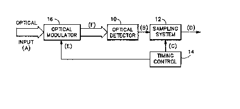
Abstract of the Disclosure
Optical detector storage effects reduction is
achieved by inserting an optical modulator between the
optical signal to be measured and the optical
detector. The modulator is normally turned off, and
is only turned on during the period when the output of
the optical detector is being sampled by a sampling
system.

Revendications

Note : Les revendications sont présentées dans la langue officielle dans laquelle elles ont été soumises.


- 5 -
WHAT IS CLAIMED IS:
1. An improved optical measurement system of the type
having an optical detector to which an optical signal
to be measured is input, the output of the optical
detector being sampled by a sampling system, wherein
the improvement comprises means for inhibiting the
input of an optical signal to the optical detector
except during the time when the output of the optical
detector is being sampled by the sampling system.
2. An improved optical measurement system as recited
in claim 1 wherein the inhibiting means comprises.
an optical modulator having the optical signal as
an input and outputting a modulated optical signal for
input to the optical detector; and
means for turning on the optical modulator only
during the time when the output of the optical
detector is being sampled by the sampling system.
3 . An improved optical measurement system as recited
in claim 2 wherein the turning on means comprises a
timing control circuit which generates a sample strobe
for the sampling system to sample the output of the
optical detector and a modulator strobe for turning on
the optical modulator, the modulator strobe being
approximately concurrent with the samples strobe and
having a pulse width greater than or equal to that of
the sample strobe.
4. An improved optical measurement system as recited
in claim 3 wherein the timing control circuit outputs
a plurality of sample and modulator strobes at a rate
determined by the storage effects decay time of the
optical detector such that samples are obtained in the
absence of the storage effects.

Description

Note : Les descriptions sont présentées dans la langue officielle dans laquelle elles ont été soumises.


~ ~3~D33~2
OPTICA~ DETECTOR ~TORAGE EFFECT5 REDUCTION
ackqround of the Invention
The present invention relat~s to optical
detectors, and more particularly to a method for
reducing the optical detector Rtorage ef~ects o~ a
high speed optical measuring 8y8tem.
High speed optical ~ignal~ are csmmonly mea~ured
by applying the signal continuously to an optical
detector and 6ampling the detector output signAl with
an electronic 6ampling ~ystem. ~ch a yste~ i~ used
in the OF150 Serie~ of Fiber optic Ti~e Domain
R~flectometer~ manu~actured by Tektronixt ~nc. of
Beavarton, Oregon. Assuming a pul~ed input, the
output of the detector at the tra~ling edge o~ ths
input pulse i~ in the ~orm of an exponent~al decay due
to the 6torage ti~e o~ the deteotor. A ~ample ~tro~
applied to the ~ampling ystem ~ro~ a timing control
during the decay portion of the detector output wiIl
re~ult in a sample output whioh has a ~igni~icAnt
srror ~rom the actual value o~ th~ ~nput pul~e. What
iS deBired i6 a method ~or reducing the e~fects o~ the
6torage time o~ the deteotor to produce ~ more
accurate value at the output.

~3~8~
, . . .
Sulrunary of the ;I:nvention
Accordingly the presant invention provide~ an
optical detector storage effects reduction method by
using an opt~cal modulator device to reflne and
improve the performance of the optical d~t~atorO An
input optical signal is input to the optical modulator
which is turned off prior to the ~ample tlme,
preventing light from reaching the optical det2ctor.
The modulator iB then turned on ~ust before or
concurrent with the beginning of a sample strobe.
Thus the optical signal iB prevented from reac~ing the
detector and creating storag~ e~fects that may distort
the electrical output signal during the 6ampling timeA
The ob~ects, advantages and other novel features
of ths present invention are apparent from the
following ~etailed description when read in
conjunction with the appended claims and attached
drawing.
Brief Description o~ the Drawing
Fig. lA is a block d-iagram of a prior art optical
measurement system.
~ ig. lB ls a timing diagram ~or the prior axt
optical measurement sy6tem o~ Fig. lA.
Fig. 2A is a block diagram of a high speed optical
measurement ystem according to the present inventionO
Fig. 2B is a timing diagram for the optical
~easurement ~ystem o~ Fig. 2B~
bescript~on of the Preferred_Embodiment
Referring now to ~ig~. lA and ~B a prior art

~3~ 3~32
optical measurement ~ystem has an optlcal detector 10
to which i~ input an optical signal, indicated by
(A). The output of the optical detector, i~dicated by
(B), is input to a ~ampling 8~8te~ 12. Tha ~ampling
6ystem 12 6amples the output of the optical detector
when triggered by a ~trobe pulse, indicated by (c),
from a timing control circuit 14. The resultiny
output from the -ampling system 12 is indicated by
(D), showing that there is an error in the mea~urement
value as opposed to the actual value o~ the optical
signal at the sampl$ng time.
Fig~. 2A and ~B 6how an optical measurement 8y6tem
having an optical modulator 16 inserted prior to the
optical detector 10. The output of the optical
modulator 16, indicated by (F), i~ then input to the
optical detector 10, the output of which 1~ sampled by
the sampl ing 6ystem 14 as in the prior art. The
optical ~odulator 16 is turned o~f pr$or to the 6ample
strobe from the timing control circuit 14. ~ust prior
to, or concurrent with, the generation o~ the sample
strobe from th timing control circuit 14, the timing
control circuit 14 applies a modulator ~trob~ pulse,
as indicated by (E), to the optical modulator 16 to
turn on the modulator and pass a port~on (F~ o~ the
optical signal (A) to the optical detector 10. The
~ample ~trobe ~C) sample~ the optical detec~or ou~put
tB) to produce the sample output (D) which now
represents the actual valu~ of the optical input (A)
at the sample time.
For multipls samples the interval between ample~,
~.e., between optical modulator turn on t~mes, is
determined by the time required to allow the fitorage
e~ects of the optical detector 10 to decay. ~l~o the
turn on ti~e o~ the optical modulator is kept as ~ort

~" ~L3~3~2
as possible, i. 2., the turn on time i6 only as long as
the ~ampling 6y6tem 12 requires to obtain the 6ample.
Therefore lf the etorage ef~ects decay time for the
~aximum valua of the opt~cal input signal 18 lOO
nsecs, then the optical ~ignal may be sampled at a 10
MHz rate.
Thus, the present invent$on provides a ~eans ~or
improving the performance of high 6peed optical
measurement systems by decreasing the e~ects o~
optical de~ector storage time through the use of an
optical modulator at the lnput of the optical
detector, the optical modulator bsing turned on only
during the sample time,

Dessin représentatif
Une figure unique qui représente un dessin illustrant l'invention.
États administratifs

2024-08-01 : Dans le cadre de la transition vers les Brevets de nouvelle génération (BNG), la base de données sur les brevets canadiens (BDBC) contient désormais un Historique d'événement plus détaillé, qui reproduit le Journal des événements de notre nouvelle solution interne.

Veuillez noter que les événements débutant par « Inactive : » se réfèrent à des événements qui ne sont plus utilisés dans notre nouvelle solution interne.

Pour une meilleure compréhension de l'état de la demande ou brevet qui figure sur cette page, la rubrique Mise en garde , et les descriptions de Brevet , Historique d'événement , Taxes périodiques et Historique des paiements devraient être consultées.

Historique d'événement

Description Date
Inactive : CIB de MCD 2006-03-11
Inactive : Demande ad hoc documentée 1996-06-16
Le délai pour l'annulation est expiré 1995-12-17
Lettre envoyée 1995-06-16
Accordé par délivrance 1992-06-16

Historique d'abandonnement

Il n'y a pas d'historique d'abandonnement

Titulaires au dossier

Les titulaires actuels et antérieures au dossier sont affichés en ordre alphabétique.

Titulaires actuels au dossier
TEKTRONIX, INC.
Titulaires antérieures au dossier
DONALD L. BRAND
Les propriétaires antérieurs qui ne figurent pas dans la liste des « Propriétaires au dossier » apparaîtront dans d'autres documents au dossier.
Documents

Pour visionner les fichiers sélectionnés, entrer le code reCAPTCHA :


Pour visualiser une image, cliquer sur un lien dans la colonne description du document. Pour télécharger l'image (les images), cliquer l'une ou plusieurs cases à cocher dans la première colonne et ensuite cliquer sur le bouton "Télécharger sélection en format PDF (archive Zip)" ou le bouton "Télécharger sélection (en un fichier PDF fusionné)".

Liste des documents de brevet publiés et non publiés sur la BDBC .

Si vous avez des difficultés à accéder au contenu, veuillez communiquer avec le Centre de services à la clientèle au 1-866-997-1936, ou envoyer un courriel au Centre de service à la clientèle de l'OPIC.


Description du
Document 
Date
(aaaa-mm-jj) 
Nombre de pages   Taille de l'image (Ko) 
Abrégé 1993-10-31 1 11
Revendications 1993-10-31 1 46
Dessins 1993-10-31 2 32
Description 1993-10-31 4 133
Dessin représentatif 2002-04-21 1 6
Paiement de taxe périodique 1994-06-12 1 130