Note: Descriptions are shown in the official language in which they were submitted.
``` 13036~39
- 1- PAT~:NT
ZERO POWER, ELECTRICALLY ALTERABLE,
NO~Vt)LATI LE I,ATC~I
Back~round of the Invention
1. Field of the Invention
The present invention relates to an electrically
alterable nonvolatile latch element which can be used
as a basic element in the construction of electrically
reconfigurable logic blocks.
2. Description of the Prior Art
Electrically erasable and programmable read only
memory devices and their different manifestations are
now being designed into new applications beyond the
traditional domain of nonvolatile memories.
Programmable logic arrays which until recently were
offered only in fusible link technology are now being
offered in nonvolatile memory technologies.
One disadvantage of fusible link technology is
that it requires substantial chip area to fabricate the
fusible link elements. Also, the programming circuitry
required to "blow" the fusible link needs to be large
because the link requires a relatively large amount of
current to flow through it to "blow" with a certain
degree of reliability.
Another technigue, known as the laser link
technique, utilizes a highly directed laser beam to
selectively separate the links in a memory circuit with
redundant rows or columns. This technique allows the
replacement of a limited number of defective memory
locations with the redundant memory locations.
A disadvantage of this technique is that it
requires substantial investment in capital equipment to
implement.
l3036as
-2- PATENT
Another ma;or drawback of the two above-mentioned
approaches is that their usefulness is limited by the
fact that they are only pre-packaging reconfigurable,
i.e. they are not in-circuit programmable.
Integrated circuit devices are now being designed
wherein nonvolatile EPROM elements are replacing the
fusible links, as in the case of programmable logic
arrays and the above-mentioned redundancy circuits.
This approach solves the problem of pre-packaging
reconfiguration, but it still suffers from high curre~t
and voltage requirements. It also requires the use of
an external power supply for programming operations and
W light for erasing one prototype configuration before
the device can be reconfigured. Thus, the flexibility
of in-circuit programming is not available with the
EPROM approach.
Several other types of nonvolatile memory
elements are disclosed in U.S. Pat. Nos. 4,328,565;
4,409,723; 4,486,769; 4,599,706. However, these memory
elements are primarily designed for high cell count
memories and are not self-sufficient in that they
require relatively complex sense amplifiers and have
relatively poor noise immunity.
Additionally, nonvolatile latch circuits have been
proposed in U.S. Pat. Nos. 4,132,904 (Harari) and
4,571,704 (Bohac~.
U.S. Pat. No. 4,132,904 discloses a
volatile/nonvolatile loqic latch circuit with a pair of
circuit branches, each comprising a field effect
transistor and a floating gate field effect transistor
connected in series. The control gates of the floating
gate field effect transistors are cross-coupled to the
common junctions of the series-connected transistors in
the other branch. This circuit can be programmed to
~ ~.,,.",,,j,,,., ,~, ..
.:~
i3036~ pPL'r~NT
assume the desired state when power is turned on and
can also be intentio~ally written over if
complementary data is to be stored.
U.s. Pat. No. 4,571,704 discloses a nonvolatile
latch circuit which assumes the proper state when power
is applied to the circuit, irrespective of the power-
applying conditions. This is accomplished by
configuring a pair of circuit branches with each branch
comprising a field effect transistor connected in
lo series with a floatinq gate field effect transistor.
The gates of the normal field effec' transistors are
cross-coupled to the common junctions between the
series transistors in the other circuit branch. Also,
the control gates of the floating gate field effect
transistors are capacitively cross-coupled to the
floating gates of the transistors in the other branch.
In the latch proposed by Bohac, if both the
nonvolatile memory transistors in the two circuit
branches are off (which is normally the case for
enhancement floating gate ~OSFETs when a device first
comes out of wafer fabrication!, then when power is
turned on, the outputs of the nonvolatile latch are
indeterminate since no pull-down to VSS is available
until after the memory elements have been programmed.
Summary of the Invention
An electxically programmable latch in accordance
with the present invention includes two basic
components: a) two nonvolatile memory cell elements and
b~ one cross-coupled static latch. The two nonvolatile
memory cell elements are metal-oxide-semiconductor
field effect transistor (MOSFET) devices which form the
two branches of the circuit module. The floating gates
~f the nonvolatile memory cell elements in the two
j ~303689
_4_ PATENT
~ranches are capacitively coupled to their respective
control gates via coupling capacitors which ~re formed
by the overlap area between the control gate and the
floating ~ate with a thin oxide dielectric fieparating
the floating gates from the control gates. In addition
to being capacitively coupled to their respective
control gates, the floating gate of one memory cell
element in one branch is capacitively coupled to the
control qate of the other memory cell element in the
other branch and vice-versa. This capacitive cross-
coupling is achieved via relatively small aroa
tunneling capacitors commonly known to those skilled in
the art as Fowler-Nordheim capacitors. The drain of
the nonvolatile memory cell element in one branch is
coupled to the input of a complementary metal-oxide-
semiconductor (CMOS) inverter, while the drain of the
nonvolatile memory cell element in the other branch is
coupled to the input of a second CMOS inverter. The
output of the first CMOS inverter is coupled to the
input of the second CMOS inverter which is also coupled
to the drain of the nonvolatile memory element in the
second branch. Likewise, the output of the second CMOS
inverter is coupled to the input of the ~irst CMOS
inverter which is also coupled to the drain of the
nonvolatile memory element in the first br~nch. The
two cross-coupled CM~S inverters form a configuration
which is commonly known to those skilled in the art as
a static cross-coupled latch. ~he cross-coupled CMOS
inverters are intended to sense the state of the two
nonvolatile memory elements in the two branches and
present the appropriate levels on the output lines.
To program the latch, data input circuitry is
employed which can selectively place either a net
positive or a net negative charge on the floating gate
~' ~13W~9
_5_ ~ATENT
of one nonvolatile memory element in one circuit branch
while simulanteously putting a net negative or a net
positive charge on the floating gate of the other
nonvolatile element in the other branch. The
nonvolatile memory element with a net negative charge
on the floating gate operates in the enhancement mode
(i.e. no current flows through the element when its
control gate is held at ground potential) and is
popularly known to be "ERASED" in nonvolatile memory
terminology. The nonvolatile memory element with a net
positive charge on the floating gate operates in the
depletion mode (i.e. current flows through the element
when its control gate is held at grDund potential) and
is popularly known to be "WRITTEN" in nonvolatile
memory terminology.
When power is removed form the device, the data in
the cross-coupled inverter latch is lost; when power is
brought back to the device, the states of the
nonvolatile memory elements in the two branches are
sensed at the inputs of the inverters which form the
cross-coupled latch. Depending on the Gtates of the
nonvolatile memory elements (which are normally
complementary to one another in the two branches of the
circuit module), the cross-coupled inverters quickly
latch in the proper state by feeding the proper voltage
level at the input of the other inverter.
Thus, the present invention offers an electrically
alterable latch which can be used in a myriad of
applications where certain functions (for example, a
~0 standard EEPRON or a standard logic chip with
nonvolatile latch elements) need to be customized to
meet particular requirements. Another possible
application is the EE-DIP switch, wherein the pins may
~303689
6 7~094-36
be reconfigurecl accordlng to desired requirements by lnputting a
certaln instruction to the device.
In a particular application, the electrlcally alterable
latch of the present invention has been deslgned into the logic
module of a reconfigurable EEPROM device ln which different
sections of the memory core array can be reconfigured to be
accessed by the outside world. This latch has also been utilized
as a building block for a nonvolatile address pointer which is
used to disable write operatlons in the user-defined section of
the memory array core. This provides security of critical data
from being accidentally written over.
According to a broad aspect of the invention there is
provided an electrically alterable nonvolatile latch element
comprising:
a) a static latch element comprising first and second
cross-coupled inverter elements wherein the output of the first
inverter element is connected to the input of the second inverter
element and the output of the second inverter element is connected
to the input of the first inverter element;
b~ a first nonvolatile storage element which stores a first
charge state, the first storage element being connected to provide
the first charge state to the input of the first inverter element
under preselected conditions; and
c) a second nonvolatile storage element which stores a
second charge state, the second storage element being connected to
provide the second charge state to the input of the second
` inverter element under the preselected conditions.
,,
`. 1303689
6a 72094-36
According to another broad aspect of the invention there
is provlded an electrically alterable nonvolatile latch element
comprising:
a) first and second nonvolatlle floatlng gate fleld effect
transistor (FET) memory cell elementsr the floatlng gates of the
memory cell elements belng capacltively coupled to thelr
respective control gates, the floatlng gate of the first memory
cell element being capacitively coupled to the control gate of the
second memory cell element, the floatlng gate of the second memory
cell element being capacitively coupled to the control gate of the
first memory cell element; and
b) a statlc cross-coupled latch lncluding first and second
invertor elements, the drain of the first memory cell element
being connected to the input of the first invertor element, the
drain of the second memory cell element being connected to the
input of the second invertor element, the output of the first
invertor element being connected to the input of the second
invertor element which is also connected to the drain of the
second memory cell element, the output of the second invertor
element is connected to the input of the first invertor element
which is also connected to the drain of the first memory cell
element.
~- According to another broad aspect of the invention there
is provided an electrically alterable non-volatile latch element
wherein the static cross-coupled latch comprises first and second
P-channel FETs and first and second N-channel FETs, the drains of
the first P-channel FET and the first N-channel FET and of the
, '
;~ ~'` ''
` :
, .
` 1303689
6b 7209~-36
second P-channel FET and the second N-channel FET, respectively,
being commonly connected, the sources of the first and second P-
channel FETs being commonly connected to a flrst potentlal, the
sources of the first and second N-channel FETs being commonly
connected to a second potential more negative than the first
potential, the gates of the first P-channel FET and the first N-
channel FET being commonly connected to the drain of the first
memory cell element and to a first output, the gates of the second
P-channel FET and the second N-channel FET being commonly
connected to the drain of the second memory cell element and to a
second output, the sources of the first and second memory cell
elements being commonly connected to the second potential.
Other objects, features and advantages of the present
invention will be understood and appreciated by reference to the
detailed description of the invention provided below which should
be considered in conjunction with the accompanying drawings.
Desc~i~tion of the DrawingLs
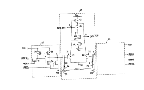
Fig. 1 is a schematic diagram illustrating a zero power,
electrically alterable, nonvolatile latch in accordance with the
present invention, together with a high voltage inverter circuit.
~ Fig. 2 is a schematic diagram illustrating a layout of
- the Fig. 1 circuit.
Fig. 3A is a cross-sectional view taken along line AA in
Fig. 2.
~- Fig. 3B is a cross-sectional view taken along line BB in
Fig. 3.
~ . ., ,,:
. .
``~ i303689
6c 72094-36
Fi~. 4 is a block dlagram illustrating a clrcuit
application in which the nonvolatile latch of the present
invention can be use~.
" 1303689
_7_ PATENT
petailed Description of the Invention
An embodiment of an electrically alterable
nonvolatile latch element in accordance with the
present invention, along with an associated high
voltage inverter circuit, is illustrated in Fig. 1.
The basic latch circuit 10 comprises two
subcircuits. The first subcircuit is a cross-coupled
static latch which includes two P-channel field effect
transistors 12 and 14 and two N-channel field effect
transistors 16 and 18. The second subcircuit includes
two nonvolatile memory transistors 21 and 22.
The drains of transistors 12 and 16 are coupled to
each other at node A. The drains of transistors 14
and 18 are coupled to each other at node B. The
sources of transistors 12 and 14 are connected to the
positive supply potential VCC. The sources of
transistors 16 and 18 are connected to the ground
potential VSS. The gates of transistors 12 and 16 are
coupled together and are also coupled to node B.
Transistors 21 and 22 are N-channel floating gate
MOSFET devices in which the floating gates are formed
in a polysilicon layer and the control gates are
selectively defined in the bulX silicon by a buried N+
implant mask. The floating gate (node C) of the
memory transistor 21 is capacitively coupled to its
control gate (node D) via coupling capacitor 24.
Coupling capacitor 24 is essentially formed by the
overlap of the floating polysilicon gate and the buried
N+ implant area exposed by the thin oxide mask, as
illustrated in Fig. 3A. Likewise, the floating gate
(node E) of the memory transistor 22 is capacitively
.~,.. . .
`` ~303689
-8- PATENT
coupled to its control gate (node F) via the coupling
capacitor 26.
In addition to being capacitively coupled to their
respective control gates, the floating gates of the
transistors 21 and 22 are capacitively cross-coupled to
the control gates of transistors 22 and 21,
respectively, via relatively small area tunneling
capacitors 28 and 30. As shown in ~ig. 3B, the
tunneling capacitors 30 and 28 are formed by the
lo overlap of the floating gates of transistors 21 and 22
with the buried N+ implant areas which are exposed by
the thin oxide mask and are electrically in common with
the control gates of transistors 22 and 21,
respectively. Both the coupling capacitors 24, 26 and
the tunneling capacitors 28, 30 have relatively thin
oxide (100 Angstroms) dielectrics between the floating
gates and the control gates.
The drain of the memory element 21 is coupled to
node B, which was defined in conjunction with the
cross-coupled static latch. Similarly, the drain of
the memory element 22 is coupled to node A, which was
previously defined. The sources of both memory
elements 21 and 22 are connected to the ground
potential VSS.
In addition to the capacitive couplings indicated
above, there are additional stray capacitances inherent
in the layout of the latch shown in Fig. 2. These
include the floating gate to control gate overlap
capacitances in the nonthin-oxide areas and the
capacitance due to the source and drain overlap to the
floating gate in the memory transistors.
Figs. 3A and 3R show the cross-sectional views of
the memory cell element along the cross-sections AA and
BB as indicated on the layout of the latch in Fig. 2.
i~O36~9 PA~E~T
In Fig. 3~, reglon 300 comprises the P-type
silicon in which the highly doped Nl source and drain
regions are formed for the N-channel CMOS transistors
Also formed in the region 300 are buried-N+ diffusions
which are not as highly doped compared to the
source/drain N+ regions. The buried-N~ regions are
used to form the control gates of the memory
transistors and can also be used for conductive
underpasses in other parts of the circuitry. The
control gates of transistors 21 and 22 are shown in
the cross-sectional diagrams of Figs. 3A and 3B. The
floating gates of transistors 21 and 22 (nodes C and
E, rèspectively) are also shown in Figs. 3A and 3B and
are comprised of conductive polycrystalline silicon.
The floating polycrystalline gate of transistor 21 is
separated from the crystalline silicon by the coupling
oxide 24, the tunneling oxide 28, the gate oxide 31,
the oxide over the buried-N+ region 301, and the field
oxide 302. The oxide over the buried Nl, region 301,
is substantially thicker than the gate oxides 30 and
32. The field oxide, region, 302, is substantially
thicker than the oxide in region 301.
In addition to the capacitive couplings "Ccoup"
and "Ctun," due to the coupling and tunneling oxides
respectively, the floating gate of the transistor 21
is also capacitively coupled to its own control gate
due to the overlap of the floating polysilicon gate to
its control gate formed by the oxide over the buried-N+
region in the silicon substrate, "Cbn+g." Another
component of the capacitance, "Cfld," is due to the
overlap of the floating polysilicon gate to the
substrate in the field oxide regions 302.
In order to program the latch, a high programming
voltage "VPPI" (12-17v) must be applied to one of the
303689
PATENT
--10--
two proqramming nodes D or F for about 5-10 ms.
Considering the case in which VPPI ~ 5 applied to node
D, then the Dther programminq node F must be held at
the ground potential. For a virgin cell with no charge
on the floatinq gate, an initial voltage equal to
Rg VPPI appears across the tunnel oxide 28, where;
R Ccoup + Cbn+g _ (l)
9 Ccoup + Cbnlg + Ctun + Cfld ~ Cgox ~ Cbn~t
where: Rg : Control gate coupling ratio of Memory
element,
Ccoup: Floating gate to Control gate
capacitance due to the coupling oxide,
Cbn~g: Floating gate to Control gate
capacitance due to the buried N+ oxide
around the gate region,
Ctun : Floating gate to Control gate of
adjacent cell capacitance due to the
tunnel oxide,
Cfld : Floating gate to substrate capacitance
due to the field oxide,
Cgox : Floating gate to substrate capacitance
due to the gate oxide,
Cbn~t: Floating gate to Control gate of
adjacent cell capacitance due to the
buried-N+ oxide around the tunnel oxide.
The initial electric field "E" across the tunnel
oxide is given by:
3 E_ RR VPPI
Ttun (2)
where, Ttun: Thickness of tunnel oxide,
:~ '
13036~39
~aTENT
--11--
VPPI: Voltage applied to the Control gate of
the memory cell.
If the initial electric field "E" is of the order
of 9-1~ Mv/cm, then a sufficient number of electrons
tunnel through the tunnel oxide onto the floating gate
of transistor 21 storing a net negative charge on node
C so as to make an appreciable positive shift in the
threshold voltage of this device. Also, the floating
lo gate of transistor 22 is capacitively coupled up to an
initial voltage equal to Rg VPPI, where:
Ctun I Cbn+t
g Ccoup ~Cbn+g + Ctun + Cfld + Cgox + Cbn~t (3)
1~
The initial electric field across the tunnel oxide
associated with the floating gate of transistor 22 is
~iven by:
E- VPPI - Ra VPPI
Ttun (4)
If the initial electric field "E" is of the order
of 9-10 Mv/cm, then a sufficient number of electrons
tunnel through the tunnel oxide out of the floating
gate of transistor 22 storing a net positive charge on
node E so as to make an appreciable negative shift in
the threshold voltage of this device.
The operation of positive threshold voltage shift
by the application of high voltage, VPPI, to the
nonvolatile memory element is known as "ERASE" and the
operation of negative threshold voltage shift-is known
as "WRITE" in EEPROM terminology.
Both the ERASE and ~RITE operations are self-
limiting. During ERASE, the initial electric field "E"
1~0368g
-12- ~ T
Nrdheim Conduction Of
he fllowing relation hi
(erase) e ~ . A . ~z ~
OWeve~ decreases with ti
ns tunnel through the t
the flating POlycryst 11
Y, the electric field ~E~ i
tunnel through the o i
age shift is negligible
peraticn, the initial
ler Nordheim
the relationship
~A ~ eXpL ~1l (6
0n th are PhYSical cOnstant
e energy barrier hei~ht
face5 and the e~fectiv
e tUnnel diel~ctric A i
tUnnel diele~ trir
"E ~ ~ TE Peration, the ele t
ses With time as more
el OXide out of the fl ti
Y leaVing the flOating t
The electric field "E'~
ery few electrons tun
nd further threshold v lt
negl igible .
D ~Ode~ the contrOl g t
Y ements (nodes D and P~)
1 and the electric fi ld
-~`` 13036E~9
PATENT
~13--
tunnel oxides are minimal and are ~nly due to the
charges on the floating gates due to the programming
operation. The tunneling of charges at these low
electric fields is negligible and this translates to
long data retention times (on the order of 10 years or
longer for Tj < or ~ 150-C). Thus, the two memory
elements in the electrically alterable latch remain
programmed to their respective ERASED (enhancement) and
WRITTEN (depletion) states. For the case when
transistor 21 is ERASED and transistor 22 is WRITTEN
(see Fig. 1), when the power is first turned on to the
device, the following sequence of events occur:
(a) Node A is pulled low because transistor 22
is ON and is in the depletion mode;
(b) Node A going low forces the inverter formed
by transistors 14 and 18 to try to force its output
high. Transistor 21 being OFF (ERASED) allows node B
to pull up towards VCC;
(c) The high going node B forces the output
(i.e., node A) of the inverter formed by transistors
12 and 16 further towards the ground potential.
Eventually, due to the positive feedback, node B
pulls up to VCC and node A is pulled down to VSS. At
this point, the two cross-coupled inverters are latched
to their proper states and no dc power is consumed by
the circuit.
For the proper operation of the latch, the
current sinking capability of the written memory
element should be such that it can pull the
corresponding cross-coupled latch node low enough to
set the latch to its proper programmed state.
The basic latch circuit 10 described above can be
used in conjunction with a high voltage inverter
circuit 20, as shown in Fig. 1.
-~ 1303689
-14- PATE~T
The purpose of the circuit 20 is to translate the
low (VSS) and high (VCC) CMOS levels at its input into
high (-VPPI 12-17v) and low (VSS) levels respectively.
~hus, during the programming mode (PROG~VCC, PROGB=VSS)
if DATAINB=low CNOS level, then node G is pulled low;
this turns N-channel MOSFET 34 OFF and P-channel
MOSFET 36 ON. This allows node D to pull up to VPPI
and turn P-channel MOSFET 38 OFF.
For the other case, when the DATAINB=high CMOS
level during the programming mode, node G pulls up
towards the CMOS high level, thereby turning
N-channel MOSFET 34 ON and P-channel MOSFET 36 OFF.
Node D is pulled down to VSS, thereby turning
P-channel MOSFET 38 ON which pulls node G towards
VPPI. Thus, circuit 20 works like a high voltage
inverter.
A similar circuit blocX 20 is also connected to
the control gate of memory element 22 shown in Fig. 1.
This circuit can be used to reset the DATAOUT (Node B)
of the nonvolatile latch to a low ~VSS) state, by
taking the RESETB signal low during the program cycle.
Fig. 4 shows one possible setup in which the
nonvolatile latch could be used.
Circuit block 30 includes an "N" bit long
register which has the nonvolatile latch circuit 10
described above as the basic building block. The
circuit block 40 includes "N" high voltage inverter
circuits 20 described above, the outputs of each
feeding into the input of a corresponding nonvolatile
latch 10 in the block 30.
In addition to the "N" nonvolatile latch elements
in the circuit block 30 and the "N" high voltage
inverters in the circuit block 40, there is one
additional nonvolatile latch element and two
' .
,
'~ . ' ' '
, ~ '
303689
~ NT
-15-
additi~nal high voltage inverters shown in Fig. 4. All
the high voltage inverters have VPPI and PROG as common
inputs. The top circuit block 20' has "PROGB" and
"PROG-DISABLEB" as the other inputs and its output
"DISABLE" feeds into the control gate of one of the
memory elements of the additional circuit block 10'.
The control gate of the other memory ele~ent in the
circuit block 10 is connected to VSS. The output
"P~OG-DISABLE" of the circuit block 10 serves as a
1~ common input to the remaining N+l high voltage
inverters. The sec~nd high voltaqe inverter 20"
outside of the circuit block 40 has its last remaining
input~connected to a signal called "RESETB" and its
output "RESET" is connected to one input of each
nonvolatile element in the circuit block 30. The last
input of each high voltaqe inverter element in the
circuit block 40 is connected to the input of the
corresponding nonvolatile latch in the circuit block 30
as shown in Fig. 4.
The transistor ratios of the cross-coupled
inverters in the circuit block 10 outside of the
circuit block 30 can be set such that the circuit
powers up with PROG-DISABLE - VSS be~ore the first
PROG-DISABLE operation is performed. This enables the
RESET operation to be performed on all the nonvolatile
elements in the circuit block 30. The RESET operation
resets all bits A0 - AN to 0s'. Next the desired bit
pattern ADDBl - ADDBN can be input to the circuit bl~ck
40 along with the other inputs VPPI (12-17V), PROG=VCC,
DISABLE - VSS valid during the program cycle. After
the programming cycle (typically 5-10 ms) the bit
pattern A0-A7 should be identical to the desired bit
pattern ADDl - ADDN that was input to the circuit
block 40.
" ~303689
~A~E~T
-16-
Once the desired bit pattern ls programmed in the
circuit block 30 is can be disabled from further
pattern changes by performing a PROG-DISABLE operation.
This is done by taking the PROG-DISABLE input to VSS
during the programming operation with RESETB and ADDBl
- ADDBN all at VCC. This operation makes the signal
PROG-DISABLE permanently high thereby disabling all
future pattern changes in the circuit block 30.
It should be noted that the example described
above is merely for illustrative purpose and is only
one of the many possible configurations which represent
the application of the present invention.
a,, ~ ., .. . ~ ..
.
,
,
.