Note: Descriptions are shown in the official language in which they were submitted.
13~3716
1 53,140
CIRCUIT INTERRUPTER APPARATUS WITH A
SELECTABLE DISPLAY MEANS
BAC~GROUND OF THE INVENTION
1. Field of the Invention:
This invention relates generally to solid-state
circuit interrupters and more specifically, to such circuit
ir,'errupters ac are utilized in molded case and metal clad
type circuit interrupters and as are capable of acting on a
number of complex electrical parameters in order to protect
the electrical conducting system and devices connected
~3C~3716
1 thereto. This invention further relates to such circuit
interrupters that allow for system user interaction so that
the number of electrical parameters can be easily and
readily understood and responded to.
2. Description of the Prior Art
The solid-state circuit interrupter is being
employed today for significantly more complex commercial and
industrial applications than was the original circuit
interrupter first introduced as a resettable replacement for
a common fusing element. Additionally, with the recent
explosion in the use and performance attributes of the
microprocessor arts along with the coincident increasing
cost advantage for such devices, the application of micro-
processor teachings to the circuit interrupter field has
brought a commensurate demand for more complex analysis,
greater performance features, and easier interaction with
the solid-state circuit interrupter while at the same time,
maintaining or improving the cost factor for such circuit
interrupters.
An existing microprocessor based solid-state
circuit interrupter is disclosed in V.S. Patent No.
4,331,997 issued to Engel and assigned to the same assignee
as the present application. This device was able to apply
microprocessor technology to existing circuit interrupters
while maintaining the supervisory control over such factors
as instantaneous protection, short delay protection, long
delay protection and ground fault protection that were found
on existing solid-state circuit interrupters such as those
that utilized discrete or other integrated circuit
electronic components. As examples of circuit interrupters
utilizing discrete components, reference is now made to U.S.
Patent No. 3,590,326 issued to Watson on June 29, 1971 and
U.S. Patent No. 3,818,275 issued to Shimp on June 18,
1974. In addition, the microprocessor based circuit
interrupter was able to incorporate display and input
monitoring techniques that provided for more accurate and
.,
~3`~3716
1 reliable interface and operation of the electrical
distribution system on which the circuit interrupter was
being utilized.
This processor based circuit interrupter also
proved advantageous in energy management systems where it
was necessary to configure the electrical distribution
system to achieve maximum energy efficiency and a minimum
circuit inte~ruption to the system as a whole. It is well
known in the field that in configuring an electrical
distribution system, a main circuit interrupter which
protects a line feeding a number of branch circuits each
having a branch circuit interrupter disposed thereon, should
have delay times assigned so that in the event of a fault in
one of the branch circuits, the associated branch circuit
interrupter would trip before the main circuit
interrupter. In this manner, the entire electrical
distribution system would not be interrupted by a fault
condition in a branch circuit and, the device or devices
which that branch circuit was feeding, would also be
protected in a more timely manner. Still other zone
interlocking conditions can be accommodated using similar
design criteria as the above example.
The microprocessor based circuit interrupter also
proved advantageous over existing circuit interrupters in
the method of selecting and adjusting the tripping
parameters. The electrical distribution system design was
greatly simplified since it was no longer required that a
trial-and-error approach to field timing the tripping
parameters be performed.
This microprocessor based circuit interrupter
though effective and certainly an advance over the then
existing circuit interrupters, did have certain limitations
that the present application addresses and overcomes. For
instance, it would have been a great advantage to have a
communication link tied to the microprocessor based circuit
interrupter so that in working with an energy management
system the circuit interrupter could be instructed from a
13¢~3716
4 53,140
remote location to perform various supervisory tasks such
- as, for example, a load shedding operation.
Another instance of a limitation of the refer-
enced microprocessor based circuit interrupter is that the
display arrangement provides for a time-multiplexed readout
of the system operating characteristics; that is, a specif-
ic characteristic was displayed on one of two numeric
displays while at the same time, a corresponding LED
located adjacent to the numeric displays was illuminated to
indicate the parameter being displayed. This numeric value
and LED would remain on for a specific time duration,
typically 3 to 4 seconds and then the next value and LED
indicator would flash on for a corresponding amount of
time. The coordination of the displayed numeric value to
the LED for each of the two separate numeric displays in
such a short time required a high level of familiarity on
the part of the system operator. This known method of
display required further special skills in that the dis-
played values were not shown in engineering units but
?O rather in a per unit relation to the rating of the specific
circuit interrupter being utilized. To comprehend the
magnitude of the displayed value, a further arithmetic
operation had to be manually performed. Finally, current
sensing was based upon peak value sensing. Such sensing,
it can be understood, does not provide as meaningful a
measure of current as true RMS sensing.
SUMMARY OF T~E INVENTION
It is therefore an object of this invention to
provide a solid-state circuit interrupter apparatus which
utilizes a microprocessor device to inexpensively and
efliciently control the current through an electrical
dis_ i~ution circuit and to provide such protec.ions as
instantaneous protection, short delay protection, long
delay protection, discriminator protection and ground fault
protection while also providing the user with an ability to
easily monitor the conditions under which these protections
.
13~3716
1 are being provided and to react to such conditions on a
timely basis.
In accordance with the principles of the present
invention there is provided a circuit interrupter including
an interrupting means which is effective for interrupting
current flow through a normally conducting electrical
circuit when a trip condition is sensed, a means for
! conditioning a current value proportionate to the current
flow such that a conditioned signal can be produced thereby,
an operating means which samples the conditioned signal and
produces operating characteristics therefrom which are
compared to corresponding tripping parameters as represented
in a trip curve, and a means for displaying and identifying
the associated operating characteristics and conditions
under which the circuit interrupter is operating and was
operating at the time of tripping. This circuit interrupter
apparatus also includes a user control element which allows
the device operator to read at his own pace, operating
characteristics such as RMS current for each phase, energy
usage and present and peak power demand. Additionally, the
circuit interrupter apparatus includes a means for sampling
the conditioned signal in order to derive the true RMS
values for the above-listed phase currents which values are
then utilized for comparison with the preselected tripping
parameters such that a tripping condition is initiated when
the measured operating characteristic exceeds the
preselected tripping parameters. The circuit interrupter
also utilizes the display means such that a historic readout
is displayed following a recognized fault or tripping
condition, such historic type readout acting as a diagnostic
tool in servicing the fault or tripping condition.
BRIEF DESCRIPTION OF THE DRAWING
Figure 1 is a perspective view of a circuit
interrupter constructed in accordance with the prior art.
~3~3716
6 53,140
Figure 2 is a perspective view of a circuit
interrupter constructed in accordance with the present
invention.
Figure 3 is a functional block diagram of the
circuit interrupter shown in Figure 2.
Figure 4 is a block diagram of a typical electri-
cal distribution system utilizing circuit interrupters of
the type shown in Figure 2.
Figure 5 is a detailed view of t~e front panel of
the circuit interrupter shown in Figure 2.
Figure Sa is a detailed view of a first alternate
front panel portion for the circuit interrupter shown in
Figure 2.
Figure 5b is a detailed view of a second alter-
nate, front panel portion for the circuit interrupter shownin Figure 2.
F~gur- 6 is a detailed schematic diagram of the
display board system shown in Figure 3.
Figure 7 is a detailed schematic diagram of the
override circuit shown in Figure 3.
Figure 8 is a detailed schematic diagram of the
fault and panel input system shown in Figure 3.
Figure 9 is a detailed schematic diagram of the
frame and plug rating system shown in Figure 3.
25Figure 10 is a detailed schematic diagram of the
backup and reset system shown in Figure 3.
Figure 11 is a de-ailed schematic diagram of the
power supply circuits shown in Figure 3.
Figure 12 is a detailed schematic diagram of the
current and voltage calibration and conversion circuits
shown in Figure 3.
Figure 13 is a schematic diagram partly in
functional block form of the communication system shown in
Figure 3.
35Figure 14 is a detailed schematic diagram of the
auxiliary power and alarm system shown in Figure 3.
`` ~3S~37~6
7 53,140
Fiyure 15 is a functional block diagram of the
80C51 microcomputer shown in Figure 3.
Figure 16 is a system flow chart for the main
instruction loop stored in the memory of the microprocessor
shown in Figure 3.
Figure 17 is a flow chart of the first function
of the main instruction loop shown in Figure 16.
Figures 18 and 18b are a flow chart of the second
function of the main instruction loop shown in Figure 16.
10Figures 19 and l9b are a flow chart for the third
function of the main instruction loop shown in Figure 16.
Figure 20 is a flow chart for the fourth function
of the main instruction loop shown in Figure 16.
Figure 21 is a flow chart of the fifth function
of the main instruction loop shown in Figure 16.
Figure 22 is a flow chart of the sixth function
of the main instruction loop shown in Figure 16.
Figure 23 is a flow chart of the seventh function
of the main instruction loop shown in Figure 16.
20.~igure 24 is a flow chart of the eighth function
of the main instruction loop shown in Figure 16.
DESCRIPTION AND OPERATION
I. GENERAL BAC~GROUND INFORMATION
A. Description and Application of a Prior Art Circuit
Interru~ter
Before discussing the description and operation
of the present invention, a brief description of the prior
art circuit interrupter will first be presented followed by
a discussion of an application of circuit interrupter
devices to a typical electrical distribution system. As
seen in Figure 1, the prior art microprocessor based
circuit interrupter 10 includes three main segments, a trip
unit segment ll, a manual control segment 12, and a charg-
ing segment 13, all disposed in a molded case housing 14.
The charging segment 13 includes a spring (not shown) which
can be used to operate the contacts (not shown) associated
with the trip coil (not shown) and a handle 15 which can
37~;
8 S3,140
manually charge the spring or an electric motor (not shown)
which can also charge the spring. The manual control
segment 12 includes a plurality of pushbuttons 16 which
control the action of the spring in relation to the con-
tacts and windows 17 through which the status of the springand contacts can be viewed.
The trip unit 12 includes an array of
potentiometers 18 which are used for selectively adjusting
the trippin~ parameters under which the circuit interrupter
is intended to operate, a group of fault indicating LED's
19 which light to indicate a cause of trip, a plug rating
element 20 which establishes the maximum continuous current
allowed through the circuit interrupter lO, and the numeric
display elements 21 with the associated indicating LED's
22. Also included on the trip unit 12 are certain control
pushbuttons 23 which may include a reset pushbutton,
ground-and-phase .est pushbuttons and a peak energy reset
pushbutton, in addition to control switches 24 for select-
ing the characteristic shapes of portions of the trip curve
and for selecting test characteristics.
In applying a circuit interrupter to an electri-
cal distribution system, whethe~ of the existing known type
or of the presently disclosed type circuit interrupter,
certain systems design criteria must be followed as will
now be described with reference to Figure 4. A typical
electrical distribution system will include at least one
energy source shown in Figure 4 in block form 25 a first
and a second source 25 and 26 which feed respective first
and second main distribution lines 27 and 28. Disposed on
the first and second main distribution lines 27 and 28 are
respective first and second main circuit interrupters 29
and 30. Also shown in Figure 4 is a tie distribution line
having disposed thereon a tie circuit interrupter 32 which
can be effective in the event that one of the first and
second main circuit interrupters has gone to a trip condi-
tion, for connecting the other of the first and second
energy sources 25, 26 thereover. Branching off from each
. . .
13~37~6
1 of the first and second main distribution lines 27 and 28
are respective pluralities of branch circuit, lines 33a
through 33d and 34a through 34d. Disposed on each of the
plurality of branch distribution lines 33a through 33d and
34a through 34d are individual branch circuit interrupters
35a through 35d and 36a through 36d which are effective for
controlling the flow of current through the plurality of
branch distribution lines 33a through 33d and 34a through
34d to a plurality of load elements 37.
As an example of the operation of these circuit
interrupters disposed on this entire electrical distribution
system, it will be assumed that a fault condition has
occurred in one of the first plurality of branch
distribution lines referenced as 33b, such fault condition
being designated as reference 38.
The fault condition 38 which may be an overcurrent
condition caused by a short circuit, must be interrupted in
as short a time as possible, preferably on the order of 50
milliseconds or less so that damage to the distribution
system can be prevented. Additionally, it is necessary that
the branch circuit interrupter 35b initiate a trip condition
in this short time so that the first and second main circuit
interrupters 29 and 30 and the tie circuit interrupter 32 do
not trip which would cut off energy to the remaining
plurality of branch distribution lines. This method of
timing the tripping sequence of a series of circuit
interrupters requires that a delay time be introduced
whereby the first and second main circuit interrupters 29
and 30 are configured to wait for a preselected period of
time before initiating a trip condition in order to allow
the affected branch circuit interrupter 33b the opportunity
to initiate the trip condition. As seen in Figure 4, the
first and second pluralities of branch circuit interrupters
33a through 33d and 34a through 34d are separated from the
first and second main circuit interrupters 29 and 30
according to a zone format with the first and second main
~.. .
~3~371~
1 circuit intecrupters being located in a first zone,
designated zone 1 and the first and second pluralities of
branch circuit interrupters 33a through 33d and 34a through
34d being located in a second zone, designated zone 2. It
can be appreciated that additional zone levels can be added
by following the same time delay principles being employed
throughout the successive zone layers.
As discussed, the first and second main circuit
interrupters wait a predetermined period of time following
sensing of the fault condition 38 in another zone; however,
in the event that the fault condition 38 persists, the first
main circuit interrupter 27 would proceed to a trip
condition following expiration of the preselected period of
time. The sensing of the fault condition 38 occurring in
the other zone, zone 2, is accomplished by sue of zone
interlocking signals which will be described hereinafter in
further detail but which can now be described here in short
as a signal transferred from the affected branch circuit
interrupter 33b to the first main circuit interrupter 29
indicating that either a short delay pickup current or a
ground fault pickup current has been exceeded. Each circuit
interrupter is capable of receiving and transmitting a
ground fault zone interlocking signal and a short delay zone
interlocking signal.
C. Characteristics of a Time-Trip Curve
In coordinating the delay times and performance
characteristics of the circuit interrupters associated with
the electrical distribution system, reference must be made
to the characteristics of a time-trip curve as can be
represented by the trip curve segments shown in Figure 5.
The time-trip curve can be generally described as a
graphical representation, using a log-log scale, of the
desired current response characteristics of the circuit
interrupter over a time period wherein the current factor is
shown on the horizontal axis and the time factor is shown on
the vertical axis as depicted in Figure. 5.
13~3716
11
l Starting at the top and leftmost portion of the
larger, main trip curve segment, specific factors relating
to a long delay protection feature are plotted and follow
generally the sloped portion of the curve. The long delay
protection feature sometimes referred to as a thermal trip
feature since it most closely resembles a thermal-type
tripping operation typically offered by predecessor non-
electronic circuit interrupters, consists of both a
selectable current factor as shown by a first current
selecting arrow 40 which corresponds to a long delay pickup
factor hereinafter referred to as the LDPU factor and along
delay time factor hereinafter referred to as a LDT factor
and which is represented by the first time selecting arrow
41. In selecting the parameters under which the long delay
lS protection feature will be provided, the first current
selecting arrow 40 indicates that the LDPU factor or
parameter selectively adjusts the trip curve along the
horizontal axis. Additionally, the LDT factor or parameter
selectively adjusts the trip curve along the vertical axis
as illustrated by the first time selecting arrow 41.
Accordingly, the limits of the long delay protection feature
are adjustable in both the X and Y axis and provide for a
long delay protection feature which follows the slope of the
first trip-curve portion 42.
In practice, the long delay protection feature
provides an I2T trip characteristic for currents exceeding
the LDPU level. It should be understood that, at higher
levels of current in excess of the LDPU level, a shorter LDT
will result.
At higher levels of current flow through the
electrical conducting circuit, it is necessary that the
solid-state circuit interrupter provide a more rapid
response than that provided by the long delay protection
feature. This more rapid response is commonly referred to
as a short delay protection feature and is characterized by
the portion of the main trip-curve segment designated as the
~3t;~37~6
1 short delay trip-curve portion 45 shown in Figure. 5. The
short delay protection feature can be selectively configured
in one of two manners, illustrated in Figure 5 as a solid
horizontal line 45a indicating a fixed time response, and a
dashed, sloped line 45b indicating an I2T response.
A second current selecting arrow 43 shown adjacent
to the short delay trip-curve portion 45 illustrates that
the current level at which a short delay trip condition will
be initiated can be adjusted, this current level commonly
being referred to as a short delay pickup factor hereinafter
referred to as a SDPU factor. Under certain conditions, as
will be described hereinafter in further detail, it is
necessary that the short delay trip condition be initiated
immediately upon sensing a current value in excess of the
SDPU factor. Other conditions utilize the fixed time short
delay trip-curve portion 4Sa. Still other conditions arise
where it is necessary to impose an I2T trip characteristics
corresponding to trip curve portion 45b. In support of this
condition, a second time selecting arrow 44 is shown
adjacent to the short delay trip-curve portion 45b.
The next level of protection offered by the solid-
state circuit interrupter is illustrated in the bottom
rightmost portion of the main trip-curve segment and is
referred to as the instantaneous trip-curve portion 47 which
corresponds to an instantaneous protection feature. At very
high levels of overcurrent through the electrical conducting
circuit, it is necessary that the circuit interrupter
initiate a trip condition as rapidly as possible, for
instance within 50 milliseconds or less of sensing the
overcurrent condition. This overcurrent level is
selectively adjustable as illustrated by the third current
selecting arrow 46 shown adjacent to the instantaneous trip-
curve portion 47.
As illustrated in the smaller trip-curve segment
shown in Figure 5, a ground fault protection feature
provides the same types of protection as does the short
13~37~6
13
1 delay protection feature; that is, a fixed time ground fault
protection is shown as the solid vertical line 48a or an I2T
ground fault protection is shown as a dashed, sloped line
48b. The ground fault protection feature provides that,
should a certain level of current be flowing through a
ground path associated with the electrical conducting
circuit in excess of a qround fault pic~up factor
hereinafter referred to as a GFPU factor, a ground fault
trip condition will be initiated. The GFPU factor or
parameter is selectively adjustable as illustrated by the
fourth current selecting arrow 49 shown adjacent to the
ground fault trip-curve portion 48a.
~ nder certain conditions, to be discussed
hereinafter in further detail, it is necessary to wait a
period of time, designated a ground fault time factor,
hereinafter referred to as a GFT factor or parameter, before
initiating a ground fault trip condition. This GFT factor
is also selectively adjustable as illustrated by the third
time selecting arrow 50O
II. SPECIFIC PHYSICAL DESCRIPTION
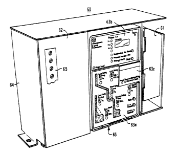
A. Circuit Interrupter
In describing the physical and operational
characteristics of the microprocessor based solid-state
circuit interrupter of the present application, reference
will first be made to Figure 2 where the solid-state circuit
interrupter 60 is shown as having three main modular
segments, an auxiliary trip segment 61, an input segment 62,
and the trip unit segment 63 which are shown mounted in a
molded insulated case housing 64.
The auxiliary trip segment 61 contains such
circuitry as an auxiliary power supply for use by the trip
unit segment 63 following interruption of the line current,
and alarm output circuitry used with external indicators.
The auxiliary trip segment circuits which provide
additional, optional features to the basic solid-state
circuit interrupter 60 can be easily and readily added or
~3~;~7~6
1 removed, will be described hereinafter in further detail
with reference to Figure 14.
The input segment 62 includes a terminal board 65 through
which various input and output signals and conditions can be
connected with the trip unit segment 63.
The trip unit segment 63 shown in Figure 2 consists
essentially of three main portions which are as follows:
the basic fault indicating and selecting portion 63a which
occupies the lower portion as shown in Figure 2; the display
board portion 63b which occupies the upper portion as shown
in Figure 2; and a rating plug portion 63 which occupies
approximately the middle right-hand portion of the trip-unit
segment 63.
Included in the basic fault indicating and
selecting portion 63a are the trip-curve segments and a
series of indicating elements, rotary switches, and push-
buttons which will be described in greater detail with
reference to Figure 5. The display board portion 63b
includes display elements and pushbuttons which are used by
the system operator to better understand and react to the
operating conditions of the solid-state circuit interrupter
60. The display elements and pushbuttons will also be
described in greater detail with reference to Figure 5.
In configuring an electrical distribution system
utilizing a number of solid-state circuit interrupters of
the type shown in Figure 2 the requirements as to the number
of options for each solid state circuit interrupter which
would provide the greatest economical advantage for that
particular configuration, can vary significantly with the
requirements of another electrical distribution system. To
that end, it is desirable to provide the greatest number of
features to the solid-state circuit interrupter 60 that are
on an optional, as needed basis so that such features can be
added or removed as deemed economically advantageous.
Accordingly, in addition to the auxiliary trip segment 61,
the display board portion 63b of the trip-unit segment 63
can also be added or removed as necessary.
"~'"
13~3716
1 In addition to the basic fault indicating and
selecting portion 63a of the trip-unit segment 63 being
essential, it is also necessary to equip the basic solid-
state circuit interrupter 60 with a plug rating portion
63c. The plug rating portion 63c establishes the maximum
continuous current allowed through the solid-state circuit
interrupter 60 and is described hereinafter in greater
detail with reference to Figure 9.
B. Description of the Block Diagram of Figure 3
The application of the present microprocessor based
solid-state circuit interrupter 60 to a particular
electrical conducting circuit as for instance one of the
plurality of branch distribution lines 33a through 33d, can
best be described with reference to the block diagram shown
in Figure 3 where the electrical conducting circuit is a 3-
phase electrical circuit connected to line terminals 70
which are associated with the terminal board 65 and lead to
corresponding three internal lines 71. Though shown as
applying to a 3-phase circuitl it is understood that the
2~ solid-state circuit interrupter 60 can be utilized with
other single-phase or multi-phase configurations.
Associated with the three conducting lines 71 are
respective line current transformers 72 and a ground current
transformer 73 which are effective for developing thereover,
current values proportionate to the current flowing in the
phase circuits and ground path circuit of the electrical
conducting circuit.
The ground current value developed by the ground
current transformer 73 is coupled to a ground current
rectifier circuit 75 for full wave rectification of the
incoming AC ground current value. Similarly, the line phase
current values are coupled to a phase current rectifier
current 74 which full wave rectifies the incoming AC phase
current values. Both the rectified ground and phase
currents are coupled to a summing circuit 76 to charge a
capacitor whose DC voltage is developed and thereafter
supplied to a power supply circuit 77. The power supply
~3~716
16 ~3,140
circuit 7~ regulates and converts this specific DC voltage
output to regulated DC voltage levels usable by the remain-
ing circuitry of the solid-state circuit interrupter 60;
such regulated DC voltage levels including but not limited
to 5 volts, 16 volts and 30 volts DC.
The power supply circuit 77 can also obtain the
specific DC voltage needed to generate these regulated DC
voltage levels from the auxiliary power circuit 61 or from
an e~ternal DC source.
The summing circuit 76 is shunt regulated by a
shunt regulating FET element 78 so that under certain
conditions, the output of the summing circuit 76 will be
shunted to ground instead of being coupled to the power
supply circuit 77.
The shunt regulating FET element 78 is controlled
at its gate terminal by a signal generated in a shunt and
chopper cor.trol portion 79b associated with a multi-purpose
- custom integrated circuit 79. Regarding the shunt and
chopper control portion 79b of the multi-purpose custom IC
79, the shunting signal is generated thus turning on the
shunt regulating FET 78 only upon sensing that the DC
voltage output of the summing circuit 76 has reached the
desired specific value thereby preventing overcharging of
the charsing capacito~ associated with the Eumming circuit
76.
Also contained in the multi-purpose custom IC 79
is a 5-volt power supply chopper control portion 79b. The
chopper portion 79b also insures that the 5-volt system
supply portion of the power supply 77 is inhibited when the
output of the summing circuit 76 is below the specific DC
voltage. In this manner, it is understood that any cir-
cui-.y o the solid-state circuit interrupter 60 reliant
upon a 5-volt supply is inhibited in the event that the
output of the summing circuit 76 is insufficient, such as
would occur upon interruption of the phase currents through
the electrical conducting circuit.
~3~37~
17
l The multi-purpose custom IC 79 also includes a
current multiplexing portion 79a. The rectified currents
are conditioned for input to the current ~ultiplexing
portion 79a of the multi-purpose custom IC 79 through a
conditioning circuit 80. The current multiplexing portion
79a is controlled by signals from the microprocessor 100 so
that a particular current signal may be selected and output
from the multi-purpose custom IC 79 upon command of the
microprocessor 100.
The selected current signal representative of the
sample value of the phase and ground current values is
coupled to a current calibration circuit 81 which allows for
an adjustment of the calibration level for current
signals. The output of the current calibration circuit 81
is designated channel 1 and is input to an Analog-to-Digital
converter 82 which can be of a commercially available type
such as for example an ADC0844 manufactured by National
Semiconductor Corp.
Similar to the current calibration circuit 81, a
voltage multiplexing, conditioning, and calibration circuit
83 is receptive of the line-to-neutral voltages of each of
the phases of the electrical conducting circuit and is
effective for calibrating voltage output signals which are
designated channel 2 and is also coupled to the A/D
converter 82.
A frame and plug rating circuit 84 associated with
the plug rating segment 63c of the trip unit generates a
plug rating signal and a frame rating signal which are
designated channels 3 and 4, respectively, and are also
coupled to the A/D converter 82.
The microprocessor 100 which controls the flow of
data through the solid-state circuit interrupter 60 is an
8-bit CMOS microprocessor which is commercially designated
an 80C51 microprocessor. The 80C51 includes a CPU and
associated ROM and RAM memories, a serial I/O port, four
parallel I/O ports and an on-chip oscillator and control
13~3716
18 53,140
circuit and is readily available in commercial quantities
from the Intel Corporation.
As shown in Figure 3, the microprocessor 100 has
associated therewitl~ four parallel I/0 ports each of which
is specifically designated ports 0, 1, 2, and 3 and which
each serve a specific purpose or function. For instance,
the port 0 is designated as the data bus 101 over which
data is transferred. As an example of the data received
over the data bus lOla, the output of the A/D converter 82
is communicated thereover upon reception of a command from
the microprocessor 100. This command is communicated to
the A/D converter 82 from port 1, lOlb of the microproces-
sor 100 by way of a control circuit 85.
Port 2, reference lOlc, of the microprocessor 100
is configured so as to receive and transmit information
relating primarily to a communications network 86 which is
effective for linking this particular solid-state circuit
interrupter 60 to a central network (not shown) which can
coordinate the operation of a number of circuit
~0 interrupters.
Port 3, lOld, of the microprocessor 100 is
configured so as to provide I/0 capabilities for general
control signals such as address control of the current
multiplexing portion 79a of the multi-purpose custom IC 79,
receipt o an override sensed signal, and control of an
external relay.
Coupled to the microprocessor 100 over the data
bus lOla is the display board system 87 which includes not
only the display board portion 63b of the trip-unit segment
63, but also the necessary circuitry to affect operation of
the display board portion 63b.
A fault and panel system 88 which includes the
fault indicating and parameter selection portion 63a of the
trip-unit segment 63 and the related circuitry to affect
the operation thereof, is also connected to the micropro-
cessor 100 by way of the data bus lOla.
13~37~6
19 53,140
Associated with the fault and panel system 88 is
- a backup and reset system 89 which provides that, in the
event of a circuit interruption and consequent interruption
of the 5-volt supply, a source of energy is available to
maintain operation of a cause o fault indication and
further provides that, when the system is stopped or
restarted, the operation of the microprocessor 100 is not
adversely affected.
A trip signal, which is initiated by the micro-
processor 100 when some type of overcurrent condition hasbeen sensed, is also communicated through the fault and
panel system 89 to a trip auctioneering circuit 90. The
trip auctioneering circuit 90 may also receive a second
trip signal which is generated from a hardware override
circuit 91. The override circuit 91 monitors the output of
the current conditioning circuit 80 and generates the
second trip signal immediately upon sensing an overcurrent
condition greater than a withstand rating of the circuit
interrupter. The trip auctioneering circuit 90 is effec-
70 tive for g~ting on a trip FET 92 when either one of the
trip signals is present.
A trip coil 93a associated with the trip mecha-
nism 93 is energized when the trip FET 92 is gated ON by
the trip auctioneering circuit 90.
Also associated with the trip mechanism 93 are
the trip contacts 93b which are disposed on the electrical
conducting lines 71 and open upon energization of the trlp
coil 93, and a manual control mechanism 93C which provides
for a manual operation of the tripping mechanism.
C. Description o the Microprocessor Block Diagram of
Figure 15
As seen in Figure 15, the micro?rocess~r 100 is
an Intel 80C51 microprocessor having an 8-bit format and
which contains a CPU segment 102 effective for manipulating
the operating instructions and data within the various
memory spaces according to a program sequence established
by a main instruction loop to be discussed hereinafter in
~3U3~
1 further detail with reference to Figure 16. The main
instruction loop resides in the program memory 103 which in
this instance is a non-volitale read only memory (ROM).
Data to be operated on by the main instruction loop is moved
into and out of data memory 104.
The timing of the microprocessor 100 is governed by
the use of an external timing device 109 which in this
instance is shown as a crystal but which can be accomplished
by various other timing methods that are within the scope of
the present application. The timing device 109 is connected
to the CPU 102 via an oscillator and timing control segment
110 .
III. ELECTRICAL DESCRIPTION
A. Display Board System of Figure 6
The display board system shown in Figure 6 provides
the electrical and electronic circuitry which corresponds to
and, in fact, operates the display board portion 63b of the
trip unit segment 63 shown in Figure 2. In relation to the
solid-state circuit interrupter 60 as a whole, the display
board system including the display board portion 63b and
associated circuitry is an optional feature and is not
essential to the provision of the basic protection and
monitoring features of the solid-state circuit interrupter
60.
When selected as an option though, the display
board system shown in Figure 6 provides the system operator
with a means of manipulating the information stored in the
microprocessor 100 to display phase current magnitudes,
ground current magnitude, present and peak demand values,
energy usage, a historical record of fault-causing
conditions. Identifying LEDS, disposed approximately
adjacent to the display element provide an indication of the
parameter being displayed.
At the center of the display board system is a
four-character alpha numeric intelligent display 120 which
is readily available in commercial quantities from
manufacturers such as Siemens and National Semiconductor.
i3~3716
21
1 The alpha numeric display 120 receives data inputs over a
plurality of input lines 121, shown in Figure 6 to be a
quantity of eight. Two control lines 122 serve to couple
signals CSl and CS2 to the alpha numeric display 120. The
control signals CSl and CS2 are generated in the micro-
processor 100 and control the data flow to the alpha numeric
display 120.
The alpha numeric display 120 operates on a 5-volt
supply and draws approximately 100 milliamps of current. An
independent source of 5-volt power is provided as an
integral component of the display board system. This supply
is isolated from the system 5-volt supply 77b to insure that
the display system does not place an excessive drain on the
system 5-volt power supply.
The independent 5-volt supply, for the alpha
numeric display 120 is derived from a regulator circuit
shown generally as reference 123. The regulator circuit 123
derives its source of power from an auxiliary power source
which can be, for example, the auxiliary power and alarm
circuit 61 shown in Figure 3. The regulator circuit 123
includes a transistor Q102 and associated components R106
and R107 which are configured so as to recognize the
presence of the auxiliary power and generate a display
enabling signal consequent thereto.
Also included in the regulator circuit 123 are the
components which actually regulate the auxiliary power to
derive the 5-volt power, those components including
transistor Q103, capacitor C103, resistor R105 and Zener
diode D109.
A display buffer element 124 is utilized in the
display board system as a means of isolating the micro-
processor 100 from the alpha numeric display 120. The
display buffer 124 is a tri-statable type buffer; that is,
the output can be one of three states, a positive state, a
negative state, and a high impedance state. The display
buffer 124 makes available at its output, for communication
over the plurality of input lines 121, the display data bits
which originate at the microprocessor.
``` ~3~137~;
22
1 The display buffer 124, however, only makes these
display bits available when the display enabling signal is
received from the regulator circuit 123. The display buffer
124 receives the data bits that it transfers to the alpha
numeric display 120 over port 0 of the microprocessor, the
data bus lOla.
Port 1, lOlb of the mic~oprocessor 100, simulta-
neous to the transmission of the data bits to the display
buffer 124, outputs a specific code to a multiplexer element
125 which serves to activate a specific identifying LED
indicative of the parameter being displayed. This labelling
multiplexer 125 acts as a 3-bit to 8-bit decoder; that is,
the labelling multiplexer 125 receives three bits of
information over port 1, lOlb, of the microprocessor 100 and
decodes this information to light an appropriate one of a
possible eight LED's. As seen in Figure 6, the solid-state
circuit interrupter 60 only utilizes seven of the possible
eight outputs of the labelling multiplexer 125 to activate
the one of seven identifying LED's which are shown on the
display board portion ~3b of the trip unit segment 63 and
labelled as phase current LED'S IA, IB and IC 126a through
126c, a ground current LED 126d, a present demand LED 127, a
peak demand LED 128, and an energy usage LED designated as
an MWH LED 129.
2S An eighth LED 130 which indicates a high load
condition for the solid-state circuit interrupter 60 is also
disposed on the display board portion 63b but is activated
by a separate high load signal. The high load LED 130 when
lit, signifies that the solid-state circuit interrupter 60
is monitoring a current value in the electrical conducting
circuit in excess of 85% of the full load rating.
Also output from port 1, lOlb of the microprocessor
100 is information to a control multiplexer 131 which
outputs the first and second control signals CS1 and SC2.
Resistors R102 and R103 are disposed in the two control
lines 122 to function as a means of further isolating the
alpha numeric display 120 from the microprocessor 100.
13~137~
~3
1 A display shunting FET Q101 and an associated
biasing resistor R101 are connected across the voltage
supply terminals V+, V- of the alpha numeric display 120 in
a manner such that the supply of the voltage to the alpha
numeric display 120 is controlled as a function of an output
of the display buffer 124.
As previously discussed, the display board system
offers a user interactive feature which allows the system
operator to selectively manipulate the display feature to
thereby obtain the desired information at a controlled,
comfortable pace.
To accomplish this function, a display step push-
button 132 is disposed on the display board portion 63b of
the trip-unit segment 63 at a position adjacent to the
identifying LED's 126a through 126d and 127 through 129 and
the alpha numeric display 120.
As seen in Figure 6, the display step pushbutton
132 when depressed, couples a low input signal to a push-
button multiplexer 133 which, when addressed by a signal
from port 3, lOld of the microprocessor 100, outputs the
condition of the display step pushbutton 132 to an input on
port 1, lOlb of the microprocessor 100. Recognition of this
display step pushbutton 132 condition effects an operation
~ithin the main instruction loop that selects a next
parameter to be displayed on the alpha numeric display 120
and to be indicated on the identifying LED's.
A second pushbutton, a demand reset pushbutton 134,
is also disposed on the display board portion 63b of the
trip unit segment 63 adjacent to the display step pushbutton
132 and further, also couples a low signal to the pushbutton
multiplexer 133 when depressed. The status of this demand
reset pushbutton 134 is also communicated over port 1, lOlb
of the microprocessor 100 upon a command received over port
3, lOld of the microprocessor 100.
The demand reset pushbutton 134 serves to reset the
value stored in memory for the peak demand figure, such peak
demand figure representing the highest power demanded over
~3~'3716
24
the electrical conducting circuit since the occurrence of
the last demand reset pushbutton actuation or since the
start-up of the solid-state circuit interrupter 60.
As previously discussed, the display board system
is an optional one and therefore in order to provide a more
cost effective, yet functionally effective solid-state
circuit interrupter, this option can be omitted. In so
providing this as an optional feature, the architecture of
the circuitry is configured so that essential components
such as the microprocessor lOO and the pushbutton multi-
plexer 133 are not disposed on the same circuit board as the
optional display board components.
In this manner, the basic solid-state circuit
interrupter 60 can be configured without the display board
portion 63b and the system circuit board (not shown) on
which the display board components are mounted but instead,
having a blank panel (not shown) in place therefor.
B. Fault and Input Panel System of Figure 7
Similar to the discussion for the display board
system shown in Figure 6, the discussion of the fault and
panel input system of Figure 7 will be made with reference
to the trip-unit segment 63 and specifically with reference
to the fault indicating and selecting portion 63a. The
trip-unit segment 63 shown in greater detail in Figure 5,
will be referenced here in conjunction with the circuit
components associated with the fault panel input system
shown in Figure 7. As the fault and panel input system is
an essential system, certain essential components previously
discussed are illustrated here as well and consequently will
utilize the same reference numbers as previously assigned.
One of the primary criteria that the fault and
input system must meet is the facility with which this
interfacing arrangement can be used and understood by system
operators who can typically exhibit capabilities and skills
over a wide range. This fault and panel system should
provide any system operator, regardless of his level of
experience or of the language that he speaks, with the
~ ~
1 ability to operate and understand this solid-state circuit
interrupter in the context of an overall electrical
distribution system.
To this end, as seen in Figure 5, the conventional
time-trip curve having the two trip curve segments is shown
having disposed on the actual curve sections, the fault
indicating LED's which correspond to the types of
protections previously discussed. For instance, a lonq
delay trip LED 140 is disposed on the long delay trip
portion 42 of the main trip-curve segment, a short delay
trip LED 141 is disposed on the short delay trip portion 45,
an instantaneous trip LED 142 is disposed on the
instantaneous trip-curve portion 47 and a ground fault trip
LED 143 is disposed on the ground fault trip-curve portion
48 of the second trip-curve segment.
Also shown on the fault indicating and selecting
portion 63a of the trip-unit segment 63 is a plurality of
rotary switches which are disposed proximately adjacent to
the portions of the main and second trip-curve segments that
they affect.
The first rotary switch 144 is ef~ective for
selecting a value for the LDPU factor, such value being
selectable from a range of current settings indicated by the
first current selecting arrow 40. A second rotary switch
145 selects a value for the LDT factor according to the
range of the first time selecting arrow 41. A third rotary
switch 146 selects the value for the SDPU factor according
to the range of the second current selecting arrow 43. A
fourth rotary switch 147 selects the value for the SDT
factor according to the range of the second time selecting
arrow 44. A fifth rotary switch 156 selects the value for
the INSTPU factor according to the range of the third
current selecting arrow 46. A sixth rotary switch 148
selects the value for the GFPU factor according to the range
of the fourth current selecting arrow 49. A seventh rotary
switch selects the value for the GFT factor according to the
range of the third time selecting arrow 50. An eighth
13~37~6
26
1 rotary switch 150 is effective for selecting test values of
both phase current and the ground current. These test
values are utilized to simulate actual current values. The
test values are acted upon by the main instruction loop only
in conjunction with the operation of a test pushbutton 151
and only under certain actual current conditions as will be
described hereinafter in further detail. Testing can be
conducted in either a trip or a no-trip mode; that is, when
the test current reaches the selected test current value,
the main instruction loop will either initiate a trip signal
or prevent initiation of the trip signal.
Disposed on the fault selecting and indicating
panel 63a adjacent to the test pushbutton 151 is a trip
reset pushbutton 152 which allows the system operator to
reset the trip condition if operating conditions so permit.
Because of the above-discussed disposition of the
fault indicating LED's 140 through 143, on the trip-curve
segments and the factor selecting rotary switches 144
through 150 and 156 adjacent to the trip-curve segments, it
can be appreciated that any system operator with an under-
standing of the characteristics of the conventional time-
trip curve can operate and understand the solid-state
circuit interrupter 60.
As seen in Figure 7, the plurality of factor
selecting rotary switches 144 through 150 and 156 are
coupled to the microprocessor 100 by way of the data bus,
lOla. The wiper of each 8-position rotary switch can
uniquely be pulled low through a rotary switch multiplexer
153. Depending on the position of the wiper, this logic "0"
will appear on only one of the eight data bus lines. By
this means, the microprocessor 100 can determine the wiper
position of each of the eight rotary switches.
13~371~
27 53,140
Also communicated over the data bus lOla is the
information needed to activate one of four cause of fault
LED's 140 through 143. This cause of fault information is
coupled to a latching element 154 which is effective in the
event of a circuit interruption causing a shutdown of the
microprocessor 100, for maintaining activation of the cause
of fault LED.
The test pushbutton 151 is effective when de-
pressed for placing a low signal onto an input of the
pushbutton multiplexer 133. When the pushbutton multi-
plexer 133 is addressed by a particular signal associated
with the test pushbutton 151, output from the microproces-
sor 100, the actuation of the test pushbutton 151 is
communicated to port 1, lOlb of the microprocessor 100.
A status LED 155 is also disposed on the fault
indicating and selecting portion 63a of the trip-unit
segment 63 to indicate that the microprocessor 100 is
operating properly. Associated with the status LED 155 is
a status FET Q202 and an associated biasing resistor R207
connected in a conventional LED driving manner.
As seen in Figure 7, a pull-up resistor network
RN201 is tied to the data bus lOla, such pull-up resistor
network RN201 being shown representatively as a single
element but in fa~t including ona resistor element for each
of ~ data bus lines.
C. Backu~ and Reset Svstem of Figure 8
The cause of fault LED's 140 through 143 provide
the basic reporting means for delivery of information to
the system operator informing him of the conditions of the
electrical conducting circuit. In using LED's to indicate
a cause of trip instead of the typical pop-up latching
indicators which required no power, it is an inherent
reguirement that a source of power be available to power
the cause of trip LED's 140 through 143 when the system
power supply 77 which is driven by line currents, has
collapsed. The backup and reset system shown in Figure 8
accomplishes this task.
~3~3716
28
1As previously discussed, the LED information for
controlling the cause of fault LED's 140 through 143 is
transmitted over the data bus 101a to the latching element
; 154 which holds the last transmitted input signal until that
information is later changed.
The latch output lines 160 which feed a high signal
to activate any one of the cause of fault LED's 140 through
143, also communicates the high signal indicating the type
of fault to a number of alarm elements which are shown in
Figure 14 as being part of the auxiliary power and alarm
circuit 61 shown in Figure 3. A long delay alarm signal is
transmitted when a long delay trip condition has occurred, a
ground fault alarm signal is transmitted when a ground fault
trip condition has occurred, and a short circuit alarm
signal is transmitted when either an instantaneous trip
condition or a short delay trip condition has occurred, such
two trip conditions being combined to form one alarm
signal. These alarm signals are buffered by a resistor
network RN203 and diodes D207 through D211 before they are
communicated to the alarm circuits of Figure 14.
Latch element 154 serves the purpose of driving the
high load LED 13Q which is lit when the solid-state circuit
interrupter 60 senses a current in the electrical conducting
circuit in excess of 85% of the maximum rated value.
Additionally, the latch element 154 provides the latching of
the trip signal thereover.
Once the tripping operation has been initiated,
however, the output of the system 5-volt power supply 77b
collapses due to interruption of the current from the
current transformers 72 and 73. In order to maintain
continued operation of the latching element 154 at all times
including following a tripping condition, a power
auctioneering arrangement is provided in the backup and
reset system. The system 5-volt power supply 77b is
auctioned with a separate fixed DC voltage source shown in
Figure 8 as being a battery 161 having a fixed DC voltage
associated therewith which is lower in magnitude than the
~3~37~
29
1 voltage output of the system 5-volt power supply 77b. In
this manner, it can be appreciated that the auctioneering
function, when the solid-state circuit interrupter 60 is
operating under normal conditions, will always be biased in
favor of the higher voltage associated with the system 5-
volt power supply 77b. By so biasing the auctioneering
function which includes a first auctioning aiode D212
disposed on the supply line from the system 5-volt power
supply 77b, and a second auctioning diode D213 disposed on
the supply line from the battery 161, the storage capacity
of the battery 161 is preserved and not depleted during
normal operating conditions.
The battery element 161 along with the second
auctioning diode D213 are disposed on the rating plug
portion 63c of the trip-unit segment 63 shown in Figure 5 so
that when the battery 161 has worn down, a replacement can
be installed without the need for disconnecting the solid-
state circuit interrupter 60 which would be required to
service an internally disposed element. In the present
application, the battery used as a 3-volt lithium manganese
dioxide watch-type battery capable of powering the cause of
fault LED's 140 through 143 for up to fourteen days
following the occurrence of a trip condition. It will be
noted that other type~ of batteries are contemplated here as
well as being within the scope of the present application.
Also disposed on the rating plug portion 63c in
association with the battery element 161 is a battery check
LED 162 and associated drive resistor R605. The battery
check LED and drive resistor R605 are disposed in series
with the battery 161 and with a lamp test pushbutton 163
which, when depressed, complete the path from the battery
161 to the ba~tery check LED 162 to indicate the status of
the battery 161.
During the transition from a normally operating
condition to a tripped condition wherein the systems 5-volt
power supply output is collapsing, it is necessary to
prevent spurious bus activity from affecting the latch
13q~3716
53,140
element 154 to the extent that a wrong cause of fault LED
could be activated or even that a failure to activate any
one of the cause of fault LED's 140 through 143 could
occur. During this transition it has been noted that a
false pulse could occur at the latch enable LE terminal of
the latch element 154.
To prevent this false pulse from initiating a
wrong or failed cause of fault indication, an FE~ transis-
tor Q204 is connected across the latch enable terminal LE
and an output enable terminal OE of the latch element 154
in such a manner that such spurious bus activity does not
cause the activation of a wrong or failed cause of fault
indication. The gate terminal of the FET Q204 is coupled
to the OE terminal of the latch element 154 so that a reset
signal, which proceeds the collapse of the system 5-volt
supply, is effective for isolating the latch element 154
from the system 5-volt supply by acting upon the output
enable terminal OE and, via FET Q204, upon the latch enable
terminal L_.
A trip reset pushbutton 152 and associated reset
circuitry is provided with the backup and reset system
which, allow- resetting of the latch element 154 so that
the cause of fault LED's 140 through 143 can be
extinguished.
An FET Q203 is connected having its drain and
source terminals disposed in series with the system reset
pushbutton 163, which pushbutton is a single-pole type. If
the system 5-volt supply is present, FET Q203 is gated ON
thereby so that when the trip system reset pushbutton 163
is depressed, the cathode of a diode D214 is coupled to
ground and a low signal is transmitted via multiplexer 133
which is recognized at port 1, lOlb of the microprocessor
lOO. When the microprocessor 100 senses the reset signal
as being low, a reset is invoked in the software and the
trip condition is cleared so that a signal can be transmit-
~3~37~;
31
l ted to the latch enable terminal LE over a diode D215thereby clearing the cause of trip condition display.
If the system 5-volt power supply has not yet been
restored, it may still be desirable to clear the cause of
fault indication. Depressing the trip reset pushbutton 163
causes a different signal path to be put into effect. This
allows the cause of fault LEDIs 140 through 143 to be reset
once the necessary information has been accumulated by the
system operator; additionally, the system operator may wish
to stop the operation of the optional alarms while he is
servicing the fault condition. Since the system 5-volt
power supply 77b is not available, FET Q204 is in an OFF
condition. Additionally, the auctioneering feature of the
backup and reset system has acted to couple the battery
voltage to an electrical junction 164 whereby, when the trip
reset pushbutton 152 has been depressed, a high signal is
coupled in series from the battery element 161, through the
electrical junction 164, through a resistor R206 and
capacitor C209, over a diode D216, to the latch enable
terminal LE of the latch element 154. A high pulse at the
LE terminal therefore enables the latch element 154 to latch
the inputs that it sees from the data bus 101a which, since
the microprocessor 100 is unpowered, are low. These low
inputs to the latch element 154 then translate to
extinguishing the cause of fault LED's 140 through 143 and
the associated alarms.
D. Plug Rating System of Figure 9
The plug rating system for the solid-state circuit
interrupter 60 which establishes the maximum allowable
ground fault current that can flow in a ground path
associated with the electrical conducting circuit includes a
hardware portion shown in Figure 9 and a software portion
represented in the flow chart shown in Figure 19.
Specification standards relating to maximum ground
fault currents for circuit interrupters which can have
breaker ratings ranging between 400 and 5,000 amps, have
37~
1 been established. Regardless of the breaker rating of the
circuit interrupter, a UL/NEC specification standard has
been set at 1,200 amps maximum. Additionally, as shown in
Figs. 5, 5A and 5B, there are various types of circuit
interrupter constructions such as for instance, the molded
case types and the metal clad types. For each of these,
there is a requirement to maintain certain current limits
which can be selected through the fault and panel system 88,
such limits and related conditions as will be discussed
hereinafter in further detail.
The trip unit 63 may be used with any of a number
of different circuit interrupters from this range of breaker
ratings. By installing the rating plug 63c in the trip unit
63, the user programs the full load current or breaker
rating into the microprocessor 100. It will be noted that
the rating plug 63c contains plug coding information 63d
relating to the type of circuit interrupter being used and
the code multipliers associated therewith. It should also
be noted that any rating plug 63c can be utilized with any
curve configuration and that the manner chosen was for
illustration purposes only.
As seen in Fig. 9, which includes an enhanced
illustration of the selecting arrangement for the GFPU
factor previously shown in Fig. 7, two resistors within the
rating plug 63c perform the function of establishing the
breaker rating. Each resistor forms one-half of a resistor
divider which produces a specific voltage at inputs CH. 3
and CH~ 4 of the A/D converter 82. A first resistor, a
frame rating resistor R603, characterizes the maximum
capability of the circuit interrupter itself, such
capability being commonly referred to as the frame rating.
A second resistor, the plug rating resistor X604,
characterizes the maximum capability of the load being
protected which is typically less than the frame rating.
The microprocessor 100 periodically performs A/D conversions
on the CH. 3 and CH. 4 inputs and, based on the results,
~3~?37~3
1 selects feo~ internal tables, a value of current to be
interpreted as the full load rating of the circuit
interrupter 60.
The GFPU factor is manually selectable by the
system operator to one of eight possible settings which are
read by the microprocessor 100 over the data bus lOla. The
particular information taken over the data bus lOla at this
time is stored in one of the data memory registers 104 for
use by a ground fault software subroutine in conjunction
with the current value representing the full load rating.
Having accumulated the information concerning the
selected GFPU factor and the rating plug value for the
particular solid-state circuit interrupter, the ground fault
subroutine shown in Figure 19 must perform decisional
operations before the selected GFPU factor can be acted upon
by the main instruction loop, such decisional operations
ensuring that the specification standards are not exceeded.
As seen in Figure 19, the flow chart illustrating
the operation of the ground fault subroutine first performs
a decision regarding whether a test operation has been
initiated by the system operator. The operational paths
associated with the decision and with the decision as to
whether the I2T type curve has been selected will be
discussed hereinafter in further detail.
The decision as to what value will be used for the
GFPU setting first requires loading the selected value for
GFPU in one register as shown in function block F303, and
loading the plug setting for the frame rating in another
register as shwon in fuction block F304. The ground fault
subroutine then first decides whether the frame rating is
equal to 5,000 amps, F305, and if so, the program proceeds
to load a value of 1,200 amps for the GFPU setting
irrespective of the se~ected GFPU setting.
If the response to decisional function block F305
is no, the ground fault subroutine then proceeds to ask for
specific frame rating values until a yes decision is
~;3C)3711~
34
1 reached, such specific frame rating inquiries being shown as
decisional function blocks F306a through F306e where
decisional function block F306e asks whether the frame
rating is 1,600 amps. If the response to decisional
functional block F306e is no, it can therefore be deduced
that the frame rating is selected as 1,200 amps or less so
that whatever GFPU factor is selected, it is within the
specification standards.
However, if the response to any of the decisional
function blocks F306a through F306e is affirmative, a second
level of decisional analysis must be pursued, this second
level corresponds to a decision as to the allowability of
the GFPU factor selected. The ground fault subroutine, upon
finding that a frame rating in excess of 1,200 amps has been
selected, must then verify that the GFPU factor selected,
when multiplied by the frame rating, produces a result which
does not exceed the 1,200 amp specification standard. For
this purpose, the second level decisional analysis can
result in either a verification of the selected GFPU factor;
that is, allowing the one selected to be acted on by the
main instruction loop, or a substitution of the 1,200 amp
maximum ground fault rating can be made in place of the
selected GFPU factor. The second level decisional function
blocks F307a through F307e employ a tabling technique based
on the setting of the GFPU rotary switch 148.
Once the ground fault subroutine has decided
whether to use the selected GFPU factor or the substituted
maximum GFPU factor, a further decision is made in regard to
comparing the GFPU factor with the actual ground fault
currents flowing in the ground path associated with the
electrical conducting circuit. Such decision and further
related decisions will be discussed hereinafter in further
detail.
E. Override Circuit of Figure 10
In addition to the previously discussed
instantaneous protection, it is also required however of the
~3~J37~i
1 solid-state circuit interrupter 60 that if a higher level of
current flow is detected through the electrical conducting
circuit than the instantaneous pickup level, such high level
of current occurring possibly by introduction of a faulty
wiring condition during installation, an immediate trip must
be initiated. Such a feature is typically referred to as a
hardware override protection and is provided for in the
present application by the override circuit of Figure 10.
Additionally, since the hardware override circuitry
]o is associated with the frame rating withstand capacity of
the solid-state circuit interrupter 60 as a whole and not
just the trip-unit segment 63, it would be advantageous to
locate the element or elements which determine the withstand
rating of the contacts 93b apart from the trip-unit segment
63. The element that determines this withstand rating,
which can be termed an override circuit pickup factor, is
installed during the manufacture of the circuit interrupter
frame since it is at this time that the override circuit
pickup factor is established.
As seen in Figure 10, the element that establishes
the override circuit pickup factor is a Zener diode 170
which has its anode terminal connected over a first plug
terminal 171 to an electrical junction 173. The cathode
terminal of the override Zener diode 170 is connected over a
second plug terminal 172 to one resistive element of a
resistor network element RN302. By so disposing the
override 2ener diode 170 between the two plug terminals 171
and 172, the override Zener diode 170 can be positioned at
the one particular location within the solid-state circuit
interrupter 60 which provides the greatest manufacturing and
maintenance accessibility.
An override auctioneering arrangement which
includes three negative voltage auctioneering diodes D317
through D319 produces an override signal at the anode
terminal of the override Zener diode 170, which override
signal is proportionate to the highest one of the phase
13~37~6
36
1 currents flowing in the electrical conducting circuit. The
override signal is a negative-going full wave rectified
voltage analog of the highest phase current and is produced
by the one bridge rectifier and associated current viewing
` S resistor at which this highest phase current is detected.
Three bridge rectifier circuits 74a through 74c and an
associated 3 current viewing resistors R314 through R316
sample the phase currents from respective current
transformers (not shown) and produce three individual
override signals which the three auctioneering diodes D317
through D319 decide as to which is the largest.
The override Zener diode 170 is selected so that
breakover occurs at the desired current level.
When the override Zener diode 170 is in a normal
operating condition, that is when a breakover condition has
not occurred, an override FET Q304 is biased so that current
flows through a first current path 174. Elements C304,
RN302, and D310 limit the magnitude of negative voltage that
may be applied to the gate of override FET Q304 to within
specification. The first current path 174 establishes a
flow of current from the +5-volt supply through a resistive
element of resistor network RN302, through the drain-source
junction of the override FET Q304 and to ground. When the
override FET Q304 is in an ON condition and current flows
through its drain-to-source junction, a current flows
through the first current path 174 so that the +5-volt level
is substantially dropped across the resistive element of the
resistor network RN3n2 and an overload trip signal is not
conveyed to ~ET 92.
When an override condition has occurred so that the
override Zener diode conducts, the gate-to-source junction
of the override FET Q304 becomes negatively biased thereby
turning OFF the override FET Q304. In this case, current
flows through a second current path 176t which provides the
flow of current from the +5-volt supply to the FET 92 via RN
302 and D308 coil 93a and causing a trip to occur. Resistor
RN 304 and capacitor C303 are included for biasing purposes.
~3~3716
37
1 Tying into the second current path 176 at a point
between the diode D308 and the gate terminal of the trip FET
92 is a software trip line 177 which has disposed thereon, a
diode D307 biased in the same manner as diode D308, so that
current can flow to the gate terminal of the trip FET 92.
The software teip line 177 communicates the trip signal from
the microprocessor 100 to the trip FET 92 when one of the
trip unit protections has been put into effect.
When a hardware override condition has occurred,
this fact must be communicated to the microprocessor 100 and
this is done using the sense line 175. With the first
current path 174 open by the fact that the override FET Q304
is in an OFF condition, current from the +5-volt supply is
diverted to the second current path 176. The microprocessor
100 recognizes the occurrence of the override trip condition
for display purposes.
F. Power Supply System of Figure 11
Since the solid-state circuit interrupter 60
includes not only electronic circuit elements that require a
+5-volt DC source for normal operation, but also components
that operate at higher voltage levels as for instance the
trip coil 93 which requires a +30 volts DC source and the
calibration elements 81 and 83 which require a +16-volt DC
source, the trip-unit segment 63 also includes power supply
circuitry which can provide essentially all of the operating
voltages necessary for the solid-state circuit interrupter
60 provided that an input source is available.
This input source is typically one supplied from
the line phase currents which are coupled to the trip-unit
segment 63 by means of the current transformers 72 and 73.
A number of full wave bridge rectifiers corresponding to the
number of phases in the electrical conducting circuit, plus
one additional full wave bridge rectifier for the ground
current, are provided in the power supply circuitry as the
primary input source. As shown in Figure 11, for a 3-phase
system, a total of four full wave bridge rectifiers are
needed, these being referenced as BRl, BR2, BR3, and BR4.
:,
,
~3~37~i
38
1 Once the phase and ground currents are full wave
rectified, they are summed at the anode of a summing diode
D313. The summed currents are then utilized for charging a
capacitor C306 to 30 volts DC, the charging of which is
shunt regulated by shunt regulating FET 78 which is under
the control of the shunt control portion 79b of the multi-
purpose custom IC 79. The shunt regulating FET 78 is gated
ON when it has been detected that the capacitor C306 has
been charged to the requisite +30-volt DC level. With the
shunt regulating FET 78 gated ON, the summed currents from
the full wave bridge rectifiers are shunted to ground and
the capacitor C306 cannot then be charged to a level in
excess of the 30-volt DC level.
A source junction point 180 connects not only the
primary input source of the summing diode D313 to the
capacitor C306 but also brings in secondary input sources
such as an external DC source and an auxiliary power source
over diode D307. The primary and secondary input sources
are auctioneered at the source junction point 180 so that
the highest one of the input sources can charge the
capacitor C306.
The shunt control portion 79b of the multi-purpose
custom IC 79 utilizes inputs from a shunt control circuit to
monitor the necessary voltage levels. This shunt control
circuitry includes components diodes D309, D310 and D311,
resistors R303 and R304 and resistive elements associated
with resistor network RN303 as well as a capacitor C307
arranged in a manner whereby specific voltage levels are
input to the multi-purpose custom IC 79 so that the custom
IC 79 can regulate the operation of the shunt regulating FET
78 thereby. Additionally, at the junction of resistors R303
and R304, a supply of +16 volts DC is available. This
application therefore utilizes the multi-purpose custom IC
79 to perform the functions of monitoring the operating
voltages and controlling the charging of a capacitor, such
functions as can also be accomplished by a conventional
` 39 ~3~37~6
1 comparator circuit, which circuit is also contemplated as
within the scope of the present aplication.
Additionally, upon sensing the proper operating
voltages at the capacitor C306 and at the inputs from the
shunt regulating circuitry, the multi-purpose custom IC 79
is further effective for controlling the operation of a +5-
volt chopper regulated power supply 77b. The chopper
regulated power supply shown in Figure 11 within the dashed
area and designated reference 77b is made up of amplifiers
Al and A2 and their associated biasing components, chopper
regulating transistor pair Q308 with associated biasing
components, and associated regulating and filtering
components, inductor L301, diodes D317 and D318, resistor
R317 and capacitor C313 and FET Q306.
In this instance, the multi-purpose custom IC 79 is
effective for enabling the output of the chopper regulated
power supply 77b only when the operating voltage at the
capacitor C306 as it is at the requisite +30-volt DC
level. In this application, however, the control of the
chopper regulated power supply 77b is accomplished using the
same signal as controls the shunt regulating FET 78. In
other words, the signal level achieved by the shunt
regulating circuitry under the control of the multi-purpose
custom IC 79 that gates ON the shunt regulating FET 78 to
maintain a +30~volt charge level at capacitor C306, also
enables operation of the chopper regulated power supply 77b.
It can therefore be appreciated that the type of
power supply that is utilized for providing a +5-volt DC
operating voltage for the electronic components of the
solid-state circuit interrupter 60 is not a critical factor,
only that the +5-volt DC output is available when the proper
operating voltages of the system are present. Additionally,
the multi-purpose custom IC 79 is not in and of itself a
critical factor to the operation of the solid-state circuit
in~errupter 60. As previously discussed, a separate
electronic circuit using a number of distinct electronic
13~`3716
1 components can be substituted for the multi-purpose custom
IC which would provide the functional characteristics of
monitoring the output voltages and providing a single signal
to control the charging of a capacitor and the enabling of a
+5-volt DC power supply.
G. Calibration and Selection Circuitry of Figure 12
The phase and ground currents, which in Figure 11
were discussed for their use in charging capacitor C306 and
sourcing the system power supply 77, are also coupled
through a current multiplexing portion 79a of the multi-
purpose custom IC 79 for providing conditioned signals which
the microprocessor 100 selects and samples to apply in the
various protection subroutines of the main instruction loop.
As seen in Figure 12, the phase and ground currents
are coupled from the current transformers 72 and 73 to the
four full wave bridge rectifiers BRl through BR4. Each
current completes the return path to its secondary winding
(not shown) via current viewing resistors R314 through R317
and in so doing, produces a negative-going full wave
rectified voltage analog of itself. Each of these voltage
analog signals is then reconverted to a current value via
resistors R310 through R313 and is presented to inputs of
the current multiplexing portion 79a of the multi-purpose
custom IC 79. The current multiplexing portion 79a is
controlled by way of a selection code transmitted over port
3, lOlc of the microprocessor so that, when commanded by the
microprocessor, the current multiplexing portion 79a outputs
a single value at terminal IOUT which is proportionate to
the current at one of its inputs. The microprocessor 100
also designates that a greater range of input current can be
digitized by the analog-to-digital converter 82 with the
final current value being rescaled back to its true value
internally.
The current output of the current multiplexing
portion 79a is coupled to a current calibration circuit 81,
which includes a current calibrating potentiometer P301 and
,.
1~3716
1 a current calibrating amplifier circuit A3 designated as
reference number 190. The output of the current calibrating
amplifier 190 is desiynated channel 1 and is input to the
analog-to-digital converter 82.
Designated channel 2 and also input to the analog-
to-digital converter 82 is a voltage signal which is output
from the voltage calibrating circuit 83. The voltage
calibrating circuit includes a voltage calibrating
potentiometer P302 and a voltage calibrating amplifier A4
designated as reference number 191. The signal which the
voltage calibrating circuit 83 acts upon is input thereto as
a multiplexed line-to-neutral voltage, such value of which
is necessary in calculating real power and energy associated
with the electrical conducting circuit.
A sign and voltage multiplexing element 192
receives the line-to-neutral voltages of each of the phases
of the electrical conducting circuit. Resistors R401 through
R406 form three voltage dividing circuits which, along with
diodes D401 through D406, function to limit the line-to-
neutral input signals and form a conditioning circuit
through which the line-to-neutral voltages must pass before
being input to the three input lines of the sign and voltage
multiplexer 192. The sign and voltage multiplexer 192
outputs a multiplexed voltage signal to the voltage
calibrating circuit 83 upon receiving a proper selection
code from the microprocessor 100. The code transmitted from
port 3, lOlc of the microprocessor 100 samples the line-to-
neutral voltage of a particular phase simultaneously to
sampling the sign of the current of that phase.
The inputs to the sign and voltage multiplexer 192
are taken from the output of the current transformers 72 at
a point before the respective full wave bridge rectifiers
associated with each of the three phases. These sign
signals are decoupled and limited by way of a coupling and
limiting resistor and diode arrangement shown in Figure 12
as including resistive elements of the resistor network
RN402 and diodes D408 through D413.
13~t3716
I The sign signal output by the sign and voltage
multiplexer 192 is communicated to a digitizing circuit
arrangement which provides a digital high or low signal
indicating the sign of the current, such digitized signal
being input to port 3, lOlc of the microprocessor 100. This
digitizing circuit includes an NPN transistor Q401 and
associated biasing components, resistors R407 and R409 and
diode D407.
~nasmuch as the real power and energy are needed
only when the display board system shown in Figure 6 has
been selected as an option, the sign and voltage multiplexer
192 and associated circuitry are optional equipment and are,
in fact, separate as well from the display board system.
The solid-state circuit interrupter 60 can be configured
having the optional display board system with the energy and
power circuitry shown in Figure 12, or it can be configured
without this circuitry. The sign and voltage multiplexer
192 and associated circuitry are, in fact, disposed with the
communication circuit and input segment 62 shown in Figure
2.
A selection multiplexer 193 is also shown as being
a part of the calibration and selection circuitry of Figure
12 and is effective for allowing the manufacturer of the
solid-state circuit interrupter 60 to deselect options which
the user does not purchase with the solid-state circuit
interupter 60. The selection multiplexer 193 is shown
having seven selection options which are selectable or
deselectable by use of jumpers J301 through J307. The
options shown as being deselectable are: short delay
protection, ground fault protection, instantaneous
protection, discriminator protection, long delay memory
deselection, in addition to a jumper selection as to which
table to use for the long delay protection feature.
As shown in Figure 5B and 5C, all of the possible
protections need not be selected for every application of
the solid-state circuit interrupter 60. When a certain
13~3716
43
1 solid-state interrupter application requires only the long
and instantaneous trip protection features, as is true in
the example shown in Figure 5B, a panel section is utilized
which shows only the long delay curve portion and the
instantaneous curve portion 47. In this instance, the short
delay protection would be deselected by inserting a jumper
at J303.
Figure 5C illustrates the situation where only long
and short delay protection is required thereby resulting in
the deselection of the instantaneous trip protection by
insertion of the J305 jumper. The selection of the long
delay memory feature allows for the decrementing of a long
delay tally factor upon sensing a condition below the long
delay pickup factor, such long delay memory feature as will
be described hereinafter in further detail.
In contrast to the voltage calibration and sign
information transmitted over the sign and voltage
multiplexer 192, the selection information is not an
optional feature and is, in fact, a circuit associated with
the required power supply circuit board.
H. Communication System of Figure 13
In configuring an electrical distribution system
having a number of solid-state circuit interrupters 60, it
is advantageous to communicate as much information between
the solid-state circuit interrupter and a central control
location (not shown) as possible, as well as communicating
such information with adjacent solid-state circuit
interrupter 60 whose operations could impact upon each other
as previously pointed out in the discussion of the zone
interlocking arrangement.
In order to have the solid-state circuit
interrupter 60 communicate with the central control location
which is remote from the solid-state circuit interrupter,
and which performs functions of load monitoring and load
, ~,
,. .
i3~37~6
44 53,140
shedding, the communication system shown in Figure 13
provides a` two-line wire communications arrangement 200.
An impedance matching circuit 201 couples the communication
system shown in the dashed area of Figure 13 as reference
86, to the line wires 200 with minimum signal loss or
distortion. A line driving circuit 202 conditions the
incoming communication signal so that the communication
signal may be acted upon by the custom communications IC
203. Similarly, an amplifier circuit 204 conditions the
communication signal which is output from the custom
communication IC 203 so that this communication signal may
be transmitted over the line wires 200 to the central
control location (not shown~.
The custom communication IC 203 is a self-
contained communication circuit whose function can also berealized with discrete components. It can be appreciated
that such an embodiment can be utilized in place of the
custom communications IC 203 without departing from the
scope of this application. An external oscillator arrange-
ment 204 is illustrated which defines the frequencies towhich the solid-state circuit interrupter 60 will respond.
The custom communications IC 203 can be pro-
grammed via a 12-bit address selection code established by
way of the shown three BCD switches SW1 through SW3 so that
each solid-state circuit interrupter associated with the
electrical distribution system can be assigned a unique
address code and thereby communicated with accordingly.
The BCD switches SWl through SW3 thereby program the custom
communications IC 203 so that only upon recognition of its
distinct address code in the incoming communication signal,
will information be communicated to the microprocessor 100.
The custom communication IC 203 is effective for
demodulating the incoming communication signal and deriving
a digital message therefrom which is read by the micropro-
cessor 100 over a serial data input to port 2, lOlc undercommand of a communication read/write signal. Also commu-
nicated between port 2, lOlc of the microprocessor and the
13~3716
1 custom communication IC 203, is an interrupt signal and a
security check signal. The security check signal allows the
microprocessor 100 to verify the integrity of the incoming
digital message and to reject that message when an error in
communications has occurred such as can occur from a noise
burst on the communications line. Various types of security
schemes are utilized for this purpose and are contemplated
as being within the present application, an example of which
is BCH error detection.
The microprocessor 100 has the ability to reclose
the breaker upon receiving a remote command over the custom
communication IC 203. A signal inverting FET Q502 and
associated biasing elements R507 and R513 provide the
capability to drive the signal needed to close a reclose
relay CR805 shown in Figure 14.
A close signal, which confirms the status of the
main contacts (not shown) of the circuit interrupter, is
multiplexed as an input of port 1, 101b of the
microprocessor 100.
Also communicated to the microprocessor 100 are the
zone interlocking signals SIN and GIN which inform the
microprocessor 100 associated with this particular solid-
state circuit interrupter 60, that a fault condition has
been sensed by another solid-state circuit interrupter. As
previously discussed, the SIN signal indicates a short
circuit condition and the GIN signal indicates a ground
fault condition has occurred and was detected by a
downstream circuit interrupter.
Similarly, zone interlocking signals SOUT and GOUT
are generated by this particular solid-state circuit
interrupter 60 and are communicated to other solid-state
circuit interrupters to indicate that this particular
circuit interrupter will initiate an interruption to clear
the fault condition. The SOUT and GOUT signals are
communicated over the latch element 154 upon receipt of this
information from the data bus 101a and the enabling of the
latch element 154.
4S-
.,
i3~371~
46
l I. Auxiliary Power and Alarm System Module of Fi~ure 14
As an optional feature, an auxiliary power supply
and alarm circuit module 61 provides a source of unregulated
30-volt DC power from a 120/240 VAC, 50/60 Hz input power
source.
As seen in Figure 14, this external AC input is
coupled to the primary windings of a step-down transformer
Tl. The secondary windings of the transformer Tl are
coupled to a full wave bridge rectifier BR701, the output of
which is filtered by capacitor C701 so that the unregulated
30-volt DC voltage can be made available at the +30V and GND
terminals associated with the auxiliary power supply 61.
Also included in the auxiliary power supply and
alarm circuit module 61 shown in Figure 14 are a plurality
of relay elements designated CR801 through CR805. The +30-
volt DC level developed by the auxiliary power portion is
coupled to one side of each of the relay elements. In order
to energize one of the relay elements CR801 through CR805,
each of which are associated with specific operating or
fault conditions such as, a high load condition; a short
circuit condition; a ground fault condition; and a long
delay interrupt condition, a signal must be received from
the latch element 154 shown in Figure 8. Upon receipt of a
high signal from the latch element 154 indicating the
occurrence of such a fault or operating condition, an FET
associated with that particular relay element CR801 through
CR805 is gated ON thus allowing the coil of that relay
element to be energized. A current recirculating diode D801
through D805 is associated with each of the coil elements.
The contacts of the relay elements CR801 through
CR805 are shown in Figure 14 according to the alarm or
operating condition that they indicate, and can be used, for
example, to drive a remote device notifying the system
operator of a fault or specific operating condition.
It will be noted that the reclose relay CR805 and
associated close contact previously described with reference
13U371~i
47
1 to the communication circuit of Figure 13 is disposed here
on the auxiliary power supply and alarm circuit 61.
IV. OPERATIONAL DESCRIPTION
A. Main Instruction Loop of Figure 16
The operation of the solid-state circuit
interrupter shown in Figure 2 will be now presented with
particular reference to the main instruction loop followed
by a specific reference to the individual function blocks
detailed in Figure 16.
The main instruction loop shown in Figure 16
illustrates not only the types of operation performed within
the microprocessor-based solid-state circuit interrupter 60
but also, the sequence in which these operations are
performed. From the point of initially connecting power to
the solid-state circuit interrupter 60, to the completion of
the 65,536th sample step, all instructions within the main
instruction loop follow the preselected sequence that allows
for the provision of instantaneous protection, discriminator
protection, short delay protection, long delay protection,
and ground fault protection all in a timely manner to
prevent damage to the load device.
As seen in Figure 16, upon recognizing a power-up
condition, the main instruction loop executes all necessary
hardware reset and system initialization operations, which
include but are not limited to initializing the ports and
registers, this reset and system initialization operation
being shown as reference T101 of Figure 16.
The main instruction loop then waits for a timer
interrupt operation which is shown as function T102. At
this time, a verification as to whether the solid-state
circuit interrupter 60 is to operate at a 50 or a 60 Hz
frequency, which is set during the manufacturing stage, is
made so that a basic sampling period can be established.
This basic sampling period is the time between successive
sets of samples of current and voltage for each of the
phases.
13~!3716
48
1 As previously discussed, it is necessary to be able
to initiate a tripping operation within a very short time
typically on the order of 50 milliseconds from the
occurrence of an overcurrent condition in order to prevent
damage to the electrical distribution system.
Counterbalancing this is the need to perform sufficient
sampling and calculating operations on the conditioned
signals to ensure that an accurate determination as to
whether to initiate a trip or not has been made. Also,
realizing that in coordinating between the sampling
frequency and the frequency of the sampled wave form, a l Hz
beat frequency must be accounted for, which in the case of
60-Hz signal requires an additional 16.67 milliseconds, the
sampling and calculating operations must therefore occur
within approximately 33.33 milliseconds after the occurrence
- of the overcurrent condition. The present solid-state
circuit interrupter 60 can also be configured to operate at
a 50-Hz frequency which simply requires a recalculation of
the l-Hz beat frequency time period, such configuration also
being contemplated as within the scope of the present
application.
In selecting the proper number of current sampling
and calculating operations, it has been determined that
eight samples would provide an accurate determination of
whether an overcurrent condition exists. The selecting of
the frequency for the external timing device lO9 shown in
Fig. 15 can be calculated knowing the number of operations
needed to execute that portion of the main program loop to
reach eight samples.
Though the above selection of eight samples
constitutes the preferred sampling scheme, it can be
appreciated that other sampling rates and external timing
frequency selections can be made without departing from the
scope of the present application.
From the timer interrupt function Tl02, the main
instruction loop proceeds to the first main program function
4 9
] designated F100 which includes the execution of subroutines
for sampling the phase currents and voltages, squaring and
summing the magnitudes of the sampled current values, and
calculating a tally of the power used.
After completing the above subroutines associated
with the first main program function 100, the main
instruction loop performs a first sample decision designated
SD100. This first sample decision SD100 asks whether 8
samples have been completed. If this is not an 8th sample,
the main instruction loop executes a series of housekeeping
chores which include checking the INCOM communication link
IC 203 ~101, checking the plug and frame rating values H102,
conducting read only memory (ROM) self-check H103, and
checking the status of the various pushbuttons H104 of the
solid-state circuit interrupter 60.
If it has been determined that this is an 8th
sample, the main instruction loop proceeds to execute the
second main program function designated as F200, which
includes executing an instantaneous protection subroutine, a
short delay protection subroutine, and the discriminator
subroutine.
Following completion of the second main program
function F200, the main instruction loop proceeds to execute
the third main program function designated F300, which
includes executing the ground fault protection subroutine.
Upon completion of the third main program function
F300, the main instruction loop proceeds to execute the
additional housekeeping chores designated F400 which
includes execution of the trip subroutine followed by a
subroutine which zeros the accumulated sums for the phase
and ground currents taken for the previous eight samples.
Following execution of the fourth main program
function F400, the main instruction loop proceeds to execute
a second sample decision designated SD200 which asks whether
64 samples have been completed. If the present sample is
not a 64th sample, the main instruction loop proceeds to
~3~ 71~;
1 return to the timer inteerupt function T102 to wait until
the next set of samples should be taken.
If the response to the second sample decision SD200
is affirmativer the main instruction loop proceeds to
execute the fifth main program function designated F500
which includes the execution of a long delay subroutine.
Upon completion of the fifth main program function
F500, the main instruction loop proceeds to execute a sixth
main program function designated F600 which includes
execution of the display subroutine followed by a zeroing of
the sums for the phase and ground currents for the
individual samples.
After completing the sixth main program function
F600, the main instruction loop proceeds to execute a third
sample decision designated SD300 which asks whether 256
samples have been completed. A negative response to the
third sample decision SD300 results in a return to the timer
interrupt function T102. If the response to the third
sample decision SD300 is affirmative, the main instruction
loop proceeds to execute the seventh main program function
designated F700 which executes the subroutine for
calculating average power and for scaling the power and
energy for use with the display subroutine.
Following completion of the seventh main program
function F700, the main instruction loop proceeds to execute
a fourth sample decision designated SD400 which asks whether
this sample is a 65,536th sample. If the answer to the
fourth sample decision SD400 is negative, the main
instruction loop is completed and proceeds to return to the
timer interrupt function T102. If the response to the
fourth sample decision SD400 is affirmative, the main
instruction loop proceeds to execute the eighth main program
function designated F800 which executes a subroutine for
determining a peak demand value for use with the display
subroutine. Upon completion of the eight main program
function F800, the main instruction loop has been completed
~3'~3716
51
1 so that the main instruction loop can proceed back to the
timer interrupt function T102 to begin the sampling sequence
over.
B. Mai Program Function F100 of Figure 17
As seen in Figure 17, the sequence of operations
performed in the first main program function F100 begins
with selecting the current in phase A designed IA, as well
as the line-to-neutral voltage associated with phase A
designed VA, for digitization, such selecting function being
designated F101. Following selection of the phase current
IA and line-to-neutral voltage VA, the subroutine proceeds
to sample the phase current IA and line-to-neutral voltage
VA via A/D channels 1 and 2 as shown in the block designated
F102. A conversion of the magnitude of phase current IA is
performed in the next function block designated at F103,
such conversion resulting in the phase current IA being
represented as a 12-bit binary number. A squaring operation
is performed on this 12-bit binary number which represents
the phase current IA squared as shown in the function block
F104. This squared value Por the phase current IA is then
added to current summations for phase A which are designated
ASUM and A8SUM and which represents a summation of 64
squared currents and 8 squared currents, respectively.
This same sequence of operations is repeated for
the currents and line-to-neutral voltages for phases B and
C. Accordingly, the function blocks F105 through F108
operate on phase B current and line-to-neutral voltage VB.
The function blocks F109 through F112 operate on phase CO
Protection features of the solid-state circuit interrupter
60 are performed as well using ground fault currents,
function blocks F113 through F116 illustrate the performance
of the above-mentioned operations on the current measured as
flowing in the ground path associated with the electrical
conducting circuit.
Following the above operations, the instantaneous
power in each of phases of the electrical conducting circuit
~3~7~6
52
1 is calculated and summed. In order to perform this
calculation as for instance on the current of phase A, the
program first fetches the value for the magnitude of current
in phase A, as well as the sign of the current, such
fetching operation being shown in function block F117.
Having already sampled the line-to-neutral voltage for phase
A, the function block F118 illustrates that the power value
can be calculated by multiplying this line-to-neutral
voltage for phase A by the current of phase A, while still
taking into consideration the sign of the current. Function
block F119 illustrates that the result of this calculation
is then added to a power tally. Function blocks F120
through F122 illustrate the calculation of the power and
addition to power tally in phase B of the system, function
blocks F123 through F124 illustrate the similar calculation
and addition for the power in phase C. Upon completion of
function block F124, the first main program function F100 is
completed so that the main instruction loop can then proceed
to execute the first sample decision SD100.
C Second Main Pro~am Function F200 of Figure 18
The second main program function F200 shown in
Figure 18 is executed following a determination by the first
sample decision SD100 that a group of 8 samples have been
completed.
Upon so determining that this is an 8th sample, the
second main program function F200, proceeds to execute the
instantaneous subroutine which begins by fetching the
squared current summations for the previous eight samples
designated A8SUM, B8SUM, and C8SUM, and which are
illustrated in function block F201. Function block F201
also serves to point to the highest of the squared current
summations designated MAXI2. The instantaneous subroutine
proceeds to perform a switch-read operation on switch 156
which signifies the instantaneous pickup selection, such
switch-read operation being designated F202.
13t?37~6
53
1 Following a determination as to which of three
instantaneous pickup tables are to be used based on the
rating plug coding 63d which reflects the frame type and the
breaker plug type as illustrated in function block F203, a
value of instantaneous pickup is selected, F204. Also
illustrated in function block F203 is the allocation of the
6th and 7th switch positions on the INSTPU SW156 as being
determinative of the limit values for the instantaneous
pickup factor for the particular type of circuit interrupter
being used, these two settings establishing the per unit
mu,ltipliers (Ml, M2) utilized in the main instruction loop
for purposes of conversion.
The instantaneous subroutine performs a comparison
operation between these two values as shown in function
block F205 and, if the MAXI2 value exceeds the instantaneous
pickup table reading, an instantaneous trip condition is
initiated as illustrated in function block F206 and F206a.
The discriminator subroutine serves the purpose of
monitoring the current conditions during initial power flow
through the circuit interrupter. For this purpose, the
discriminator subroutine only operates during the first few
cycles, and is bypassed thereafter until a subsequent
initial power flow occurs. It should also be noted that
initial power flow is detected as the onset of a pre-
selected minimum current value in the electrical conductingcircuit.
Function block F207 illustrates the minimum current
value that will initiate operation of the discriminator
subroutine as 0.1 per unit. A failure to meet this minimum
current value results in a zeroing of a discriminator count
designated DCOUNT, F207a. If this value has been exceeded,
the discriminator subroutine proceeds to execute the
discriminator protection and increment the discriminator
counter DCOUNT until a value of ~ is reached, F208. If the
value of DCOUNT has reached the value of 4, the function
block F208 directs the sequence of operation to terminate
37~6
54
1 the discriminator protection. Discriminator protection
consists of comparinq the MAXI2 value to a preselected
current value, in this case 11 per unit, such check function
being shown as function block F210. If the MAXI2 value
exceeds the preselected value, a discriminator trip is
initiated, F211.
The short delay subroutine, since it is related to
an optional short delay protection feature, must first
verify that the short delay protection feature has been
selected by checking the jumper J303 associated with the
selection multiplexer 193. If this checking operation F211,
results in a determination that the short delay protection
feature has not been selected, the second main program
function F200 is completed.
If the short delay protection feature has been
selected, a switch-read operation F212, is performed on the
short delay switch 146 and, depending upon a determination
as to the rating plug coding 63d which reflects the frame
type and the breaker plug type, F213 for the solid-state
circuit interrupter 60, one of three short delay pickup
table settings SDPU is identified, as shown in F214.
Similar to the allocation of switch positions 6 and 7 on the
INSTPU SW156, the 6th and 7th switch positions for the 5DPU
switch 146 determine the short delay current limits for the
particular type of circuit interrupter. The information
conveyed by the 5DPU switch 146 includes 6 fixed settings
and the 2 variable settings, which when selected, have
values as marked on the rating plug 63c.
This short delay setting SDPU is then compared,
F215, with the MAXI2 value. If the value MAXI2 is less than
the SDPU setting, the short delay subroutine ensures the
absence of the SOUT signal, F21Sa, then zeros a short delay
tally count STALLY, F215b, and then proceeds to the end of
the second main program function F200.
When the MAXI2 value is greater than or equal to
the SDPU setting, an instruction to issue the SD interlock
3~3~3716
1 signal SOUT is executed, F216. Rather than initiating a
short delay trip condition at this time, the short delay
trip subroutine first determines whether the short delay
interlock signal SIN is present, F217, which would indicate
that the short delay fault condition has been identified by
another solid-state circuit interrupter. Absent receiving
this short delay interlock input signal, SIN, the short
delay subroutine, then proceeds to inquire whether this is
the second consecutive recognition of the short delay
condition, F218. The requirement of two consecutive
recognitions of this condition therefore prevents the
occurrence of a false initiation of the short delay trip
condition which may be due to noise conditions.
In contrast to the rapid initiation of the short
delay trip condition when the short delay fault has occurred
at the present location, in the absence of an active SOUT
signal, an active SIN signal results in the execution of a
time delayed response to the detected short delay fault
condition.
Under the time delayed portion of the short delay
subroutine, the response can be either of the I2T type F220
of fixed time, F222. If an I2T response has been selected,
which corresponds to the dashed, sloped short delay curved
portion 45b shown in Figure 5, a short delay tally
designated STALLY is calculated, F221, for use in comparing
with a short delay tally limit designated STALLY LIMIT which
iS 3 preselected value taken from a short delay tally table,
according to the selection of the SDT factor as read from
the SDT switch 147, F223.
The STALLY value for the I2T response is calculated
based on the relationship STALLY = STALLY + MAXI2 where the
resultant STALLY equals the previous STALLY incremented by
the MAXI2 factor. In the event the comparing function F224
determines that the measured STALLY is equal to or exceeds
the STALLY limit, a short delay trip condition is initiated
F225, and the second main program function is ended.
~3~J3716
1 If the I2T response has not been selected, the
measured STALLY factor is determined by the relationship
STALLY = STALLY + lOPU2, and this value is then compared to
the STALLY limit to determine whether a short delay trip
should be initiated. The calculation for the measured
STALLY under function block F222 results in a fixed time
trip corresponding to the response curve shown in the solid,
vertical short delay curved portion 45a of Figure 5.
D Third Main Pro ram Function F300 of Figure 19
g
Upon completion of the short delay subroutine, the
main instruction loop proceeds to execute the third main
program function F300 which performs the operations of
selecting a proper ground fault setting GFPU and using this
ground fault setting for comparing with the measured ground
fault value to determine if and when a ground fault trip
condition should be initiated.
As seen in Figure 19, the ground fault subroutine
first verifies via a check of jumper 3304 from the selection
multiplexer 193 whether the ground fault protection feature
is, in fact, utilized in this application. If the ground
fault protection feature has not been selected, the main
instruction loop proceeds to the next main program function.
When this feature has been selected, the ground fault
subroutine will inquire whether the operator has requested a
test operation, F301 and if so, whether the measured ground
fault current at this time is equal to or greater than a
predetermined threshold value, F302. If such a ground
current is detected, the subroutine disregards the request
for a test operation, F302a. However, if this ground fault
current is below the threshold level, a switch-read
operation F321 is performed on the test rotary switch 150 to
select a test value with this value being substituted into
the comparison operation to determine whether a ground fault
trip condition should be initiated F322.
If the test operation has not been called by the
operator, the ground fault subroutine performs a switch-read
i3U371~;
1 operation, F303, on the GFPU switch 148 and this value is
utilized to fetch a ground fault pickup value GFPU for use
in the subsequent operation.
Followinq the determination of this GFPU value, the
ground fault subroutine selects the plug rating value from
channel 3 of the A/D converter 82 and then executes the
portion of the program which verifies that the selected GFPU
value is within the UL/NEC specification standards.
The comparison operation, F309, is performed
between ~he measured ground fault current value taken from
the summation of the ground currents for the previous eight
samples which is designated G8SUM, and the selected GFPU
value. A ground interlock output signal GOUT is issued if
the G8SUM value equals or exceeds the GFPU setting, F310.
If the GFPU factor has been exceeded, a check is first made
to see whether a ground fault interlock signal GIN has been
received from another solid-state circuit interrupter
F311. If such GIN signal has been received, the ground
fault subroutine performs a time delayed response similar to
that performed in a short delay protection, F314. If the
GIN signal has not been detected, the ground fault
subroutine executes the same type of rapid trip response as
is executed in the short delay subroutine. That is, a
second consecutive occurrence of ground overcurrent must be
detected, F312, in order to initiate a ground fault trip
condition, F313, thus preventing a false trip in the event
that the first occurrence was a result of noise.
Also similar to the short delay subroutine, when a
GIN signal has been received, the ground fault subroutine
executes a time delay response that can be either an I2T
response or a fixed time response, F314. If an I2T response
has been selected which corresponds to the dashed, sloped
ground fault curved portion 48b of Figure 5, a ground tally
value GTALLY is calculated, F315, using the relationship
GTALLY = GTALLY + G8SUM. If the I2T response has not been
selected, GTALLY i5 calculated as GTALLY = GTALLY + 0.625
13U3716
58
1 PU2, F316. A GTALLY limit is selected as a function of the
GFT switch, 149. The comparing operation of the calculated
GTALLY with the GTALLY LIMIT, F317, provides the
determination as to whether or not to initiate the ground
5 fault trip condition F313. It should be noted that the
GTALLY measure does not go to zero following a determination
that G8SUM has fallen below GFPU. Instead, the GTALLY
figure, upon occurrence of a G8SUM value less than GFPU
value, is decremented by a specific factor defined by the
relationship GTALLY = GTALLY - 0.25 PU2. This enables the
ground fault subroutine a means to handle arcing ground
faults.
E. Fourth Main Program Function F400 of Figure 20
Having executed the subroutines which put into
effect the various protection features such as the
instantaneous protection, discriminator protection etc. the
operation of converting this initiated trip condition into
an operation that actuates the trip mechanism and displays
the necessary cause of fault information remains to be
performed. This conversion operation is performed by the
fourth main program function F400 shown in Figure 20 which
includes primarily the trip subroutine.
The trip subroutine first determines whether the
trip flag has been set, F401, the trip flag being the
particular bit within the programmed bit assignments that is
activated by any one of the protection subroutines which can
initiate a trip condition. If it is determined that the
trip flag has not been set, the trip subroutine will proceed
to clear the contents stored for the accumulated squared
phase currents and ground current taken for the previous
eight samples, these accumulated currents being designated
the A8SUM, B8SUM, C8SUM and G8SUM, and following this, to
proceed to the end of the fourth main program function
F400. If it is determined that the trip flag has been set,
the trip subroutine then determines which protection
subroutine has initiated the trip condition and lights the
appropriate cause of fault LED thereby.
13(~37~6
59
1 If the trip flag has been set by the instantaneous
subroutine, the plug checking subroutine, the discrimina~or
subroutine, or the override subroutine an LED designated
LED4 is lit. If a short delay trip condition has been
detected, an LED designated LED3 is lit. If a ground fault
trip condition has been detected, an LED designated LED2 is
lit. If a long delay trip condition has been detected, an
LED designated LEDl is lit in either a continuous or
blinking manner conditioned upon whether a long delay trip
condition has occurred, or whether a condition approaching a
long delay trip condition is existent. Following the
determination as to which protection feature initiated the
trip condition, the trip subroutine then proceeds to set the
trip output port to 1 which thereby enables actuation of the
trip mechnism 93. With the trip output port now set high,
the trip subroutine is complete.
F. Fifth Main Program Function F500 of Figure 21
The fifth main program function F500 which consists
essentially of the long delay subroutine, is executed only
upon detection that the main instruction loop has completed
a group of 64 samples, this determination being made by the
second sample decision SD 200 shown in Figure 16.
Following the completion of the first 64th sample
group, the fifth main program function initiates an
instruction for turning off the reclose relay driver,
thereby limiting the duration of reclose relay activation to
approximately 1/4 second.
The first operation, F503 performed by the long
delay subroutine is the fetching of the MAXI2 value
previously determined during the execution of the first main
program function F100. After determining that the long
delay protection feature has been selected, the long delay
subroutine then fetches an LDPU value according to the
setting of the LDPU switch, 144 and the selection of a first
or a second long delay table determined by checking whether
a long delay table jumper J301 or J302 associated with the
selection multiplexer 193 has been selected.
13U3716
1 A comparison between the MAXI2 value previously
fetched and the LDPU factor just fetched then determines
whether an LDPU flag should be set or whether an alternate
long delay subroutine path should be taken that determines
whether the LDPU factor is being approached which would
merit lighting the High Load LED.
If the LDPU factor has been equalled or exceeded by
the MAXI2 value, the LDPU flag is set and a long delay tally
designated LTALLY is calculated as LTALLY = LTALLY +
MAXI2. The resultant LTALLY value is then used in a
comparison with the LTALLY LIMIT which is determined as a
function of a reading of the LDT switch 145. If the
resultant measured LTALLY exceeds the LTALLY LlMIT, a long
delay trip condition is initiated and the fifth main program
function F500 is then ended. If the resultant LTALLY is
less than the LTALLY LIMIT, the fifth main program function
F500 is ended without initiating a long delay trip
condition.
If the LDPU flag has not been set as occurs when
the MAXI2 value is less than the LDPU factor, the long delay
subroutine follows the alternate program path that
determines whether the MAXI2 value is equal to or in excess
of 85% of the LDPU factor. If so, the ~igh Load LED is lit;
if not, the LDPU flag is cleared. This alternate program
path of the long delay subroutine then determines whether a
long delay memory feature has been selected via the
selection jumper J307 associated with the selection
multiplexer 193. If the long delay memory has not been
selected, the factor LTALLY is cleared following the
clearing of the LDPU flag. If the long delay memory feature
is selected, similar to the situation of the ground fault
tally, GTALLY, the long delay tally, LTALLY, is decremented
so that in the event of a sporadic occurrence of the MAXI2
value exceeding or being equal to the LDPU factor, the
LTALLY factor some will retain some non-zero value. The
decrementing of LTALLY is done using the relationship LTALLY
13U371~i
6]
1 = LTALLY - 1 pU2 with a lower limit of zero. Following this
decrementing operation the fifth main program function F500
is complete and the main instruction loop can then proceed
to execute the sixth main program function F600.
G. Sixth Main Proqram Function F600 of Figure 22
Also executed after the 64th sample is the sixth
main program function F600 which includes primarily the
display subroutine shown in Figure 2.
The first function executed in the display
subroutine is the determination of whether a trip flag is
set, F601. If it has been determined that a trip condition
has been initiated, the display subroutine then determines
if a no-cause-of-trip flag is set, F602. If the no-cause-
of-trip flag is set, the display subroutine proceeds to
display any existing warning message, F604, if necessary.
If the no-cause-of-trip flag is not set, the display
subroutine displays any existing cause of trip messages
F603. The types of warning messages displayed in order of
priority by function F604 correspond to RAM failure, ROM
failure, plug failure, negative power condition, and long
delay pickup condition.
If no warning or trip messages are warranted, the
display subroutine selects the parameter to be displayed,
which can be one of the following: RMS phase currents, peak
demand value, present demand value, or energy. This
selection is ultimately under user control via manipulation
of the display step pushbutton 132.
Once selected, the parameter to be displayed is
first scaled and output, F606, to the alpha-numeric display
element 120. Once this information is output to the
display, the display subroutine performs housekeeping chores
such as clearing the individual phase current summations
designated ASUM, BSUM and CSUM. At this time, the display
subroutine is completed, as is the sixth main program
function F600 so that the main instruction loop can then
proceed to execute a third sample decision SD300 which is
shown in Figure 16.
13~3716
62
1 H. Seventh Main Program Function F700 of Figure 23
-
Having determined that the ~ain instruction loop
has completed a 256th sample or a multiple of 256, the
seventh main program function F700 which includes primarily
5 a scaling subroutine for scaling the power and energy, is
- executed.
As seen in Figure 23, a power scaling subroutine
first fetches, F701, a PTALLY value which is a summation of
the instantaneous phase power values.
The power scaling subroutine then verifies via
instruction F702, that a positive PTALLY value is present,
the alternative being that otherwise a negative power flow
is occurring which would then result in the setting of the
negative power flag so that this information can be
displayed. If a negative power situation is detected, the
power scaling subroutine then performs a two's complement
operation upon PTALLY to produce a positive equivalent
value, F704. Power scaling calculates the average power as
P-AVE/4 = PTALLY (256 X 2) and then zeros the value PTALLY,
F705.
Before scaling the calculated average power values,
the power scaling subroutine first determines whether a trip
flag has been set and that if it has, to save the previously
calculated values of power and energy so that a history
display will include these parameters and prevent alteration
for the duration of the trip event.
If no trip has occureed, the power scaling
subroutine then fetches a power scale factor designated Y
from a power scale table and scales the P-AVE/4 value
according to the relationship P-AVE = P-AVE/4 x Y/220 which
calculation yields average power value displayed as MW-H.
Having thus completed the power scaling subroutine,
the seventh main program function F700 proceeds to execute
the energy scaling subroutine. Similar to the first
instruction for the power scaling subroutine, the energy
scaling subroutine first determines whether a test flag has
13(~37~6
63
1 been set so that if it has been set, the existing scaled
energy value will not be effected by the test value, the
presence of a test flag therefore resulting in the
completion of the energy scale subroutine and the seventh
main program function F700. However, if a test is not
active, the energy scaling subroutine proceeds to fetch the
energy scale factor designated Z from a table of energy
scaling factors. Having this energy scale factor Z, the
energy scaling subroutine then fetches the P-AVE/4 factor
and proceeds to calculate the energy tally value designed
ETALLY by use of the equation ETALLY = ETALLY + P-AVE/4 x
Z. Before presenting this scaled energy tally value for
display, the energy scaling subroutine must first determine
whether this calculated ETALLY value exceeds a predetermined
limit which is established as a function of the display
capabilities of the alpha numeric display 120. In this
instance, this ETALLY limit is established as 99.g MW-H
which measure represents megawatt hours. If the ETALLY has
exceeded the ETALLY limit, the energy scaling subroutine
zeros the ETALLY and proceeds to create a fresh ETALLY value
which is then made available for display. With the
completion of the energy scaling subroutine, the seventh
main program function F700 is completed so that the main
instruction loop can proceed to execute a fourth sample
decision where it is determined whether or not the main
instruction loop is in a 65,536th sample.
I. Eighth Main Program Function F800 of Figure 24
If the main instruction loop has determined that
this is a 65,536th sample interval the main instruction loop
executes the eight main program function which primarily
performs the task of scaling the peak demand value for
display. This peak demand subroutine first executes a fetch
operation for a present demand tally designated DTALLY which
was calculated as the sum of 256 PAVE valued which are
available at the 256th sample intervals. The peak demand
subroutine then divides the DTALLY figure by 256 to
13~371~
64
1 determine the average present demand value that has occurred
over the previous 65,536 samples. It should be noted at
this time that the completion of the 65,536th sample
correlates approximately to the completion of a five-minute
interval since the calculation of the last peak demand
value. The peak demand subroutine then executes an
operation whereby the latest measured demand value
designated DTALLY is compared with the peak demand tally
designated PDTALLY which is held in storage and represents
the highest demand value recorded since power up. If it is
determined that the existing peak demand tally is less than
the latest calculated demand tally, the latest present
demand tally is then retained and becomes the new peak
demand value. If the present demand tally does not exceed
the existing peak demand tally, the existing peak demand
tally is retained. The peak demand subroutine then zeros
the present demand tally DTALLY and completes the execution
of the eighth main program function as well as the
completion of the main instruction loop so that the sequence
of sampling events can be restarted.
Although the hereinabove described embodiment
constitutes a preferred embodiment of the invention, it
should be understood that modifications may be made thereto
without departing from the scope of the invention as
detailed in the appended claims.