Note: Descriptions are shown in the official language in which they were submitted.
1:~03745
APPARATVS AND METHOD FOR DATA IND~CED CONDI~ION SIGNALING
--1--
BACRGROUND OF THE INVENTION
l. Field of the Invention
This invention relates generally to data
processing systems and, more particularly, to a
technique in a data processing system for efficiently
invoking a control program based on a predetermined
signal in a specified register location.
2. Description of the Related Art
As data processing system programs have become
larger and more complex, errors in the program have
become increasingly hard to identify. The invalid
memory reference remains one of the most common
programming errors whether reading or writing an
invalid address. For example, an array A(i,j) can
have the requirement that 0<i,j<99. However, an
attempt can be made to utilize an index (address)
outside of this range. And the invalid address
reference most often occurs when the referenced
address is part of an array field. Therefore, during
program execution, it is important that array
addresses be tested to insure that they are within
the boundaries of the array. In the past, the
program has been provided with extra code to test the
array addresses and, when an error, is encountered to
call an appropriate responsive subroutine. The
additional code for the testing of the array
addresses has resulted in programs that are greatly
a~
~3037~5
-2s
increased in size and which execute at a
correspondingly slower rate.
The problem of the testing of array addresses is
part of a more general problem of testing a Boolean
value and generating an exception when the result is
false. Other applications, in addit~on to the
testing of array addresses, include program
assertion, testing for procedure success/failure
return status and other Boolean tests for which
current procedures involve unacceptable program
(code) size and/or inefficient program execution.
A need has been felt for a technique that can
expedite execution and reduce the program code (size)
for programs, such as a program which tests array
addresses, that can test Boolean values and generate
an exception when the Boolean value is false.
FEATURES OF THE INVENTION
It is an object of the present invention to
provide an improved data processing unit.
It is a feature of the present invention to
provide an improved method of efficiently invoking a
control program based on a predetermined signal in a
specified register location.
It is still another feature of the present
invention to provide a Fault on Low Bit instruction,
the presence of a signal in the low bit field of a
register indicating de~ection of a false Boolean
~30374S
-3-
value.
It is a further feature of the present invention
to test a Boolean condition by determining the
presence of a particular bit in register location.
SUMMARY OF THE INVENTION
The aforementioned and other objects are
accomplished, according to the present invention, by
providing a data processing system with a Fault on
Low Bit Clear (FLBC) instruction. Prior to execution
of this instruction, a comparison operation is
executed to generate a Boolean value. The comparison
operation sets or clears the low bit in a specified
scalar register, determined by the validity of the
comparison operation. In the FLBC instruction, the
selected register is tested and if a false Boolean
value is found stored therein, the presence of a
fault condition is signaled to a fault control
program. This instruction eliminates the need for a
branch around a code sequence that results in a call
to an error subroutine specifying the condition
resulting in the fslse Boolean value. In the
preferred embodiment, the FLBC instruction is
selected so that a field of the instruction can be
used to pass information to the fault control
program. This instruction results in faster
execution time (no branch around subroutine call) and
less program code is required to provide the
1303~45
- 4 - 61051-2184
operation. The impact of this single instruction on the program
execution time is minimal, permitting for example greater use of
the array address checking. Apparatus is provided to supply the
data processing unit issue unit with a copy of the register bit so
that the register bit location can be checked without use of an
execution unit.
In accordance with a broad aspect of the invention
there is provided a method of controlling a processor in a digital
data processing system as it is processing instructions in an
instruction stream, comprising the steps of: generating, during
processing of an instruction in said instruction stream, a condi-
tion flag indicating whether a fault condition exists and storing
said condition flag in a preaetermined location in said processor;
executingt following generation of said condition flag, a fault
instruction which tests the condition of said condition flag and
executes a fault instruction sequence in response to said condi-
tion flag indicating a fault condition, and otherwise executing
the next instruction in said instruction stream in response to
another condition of said condition flag.
In accordance with another broad aspect of the invention
there is provided a digital data processor for processing instruc-
tions in an instruction stream, instructions comprising said
instruction stream including a condition instruction type and a
fault instruction, said processor including:
A. condition instruction execution means for generating,
during processing of an instruction in said instruction stream of
A
130374S
- 4a - 61051-2184
said condition instruction type, a condition flag indicating
whether a fault condition exists and storing said condition flag
in a predetermined location in said processor;
B. fault instruction execution means responsive to a
subsequent fault instruction for testing the condition of said
condition flag and executing a fault instruction sequence in res-
ponse to said condition flag indicating a fault condition, and
otherwise enabling said processor to execute the next instruction
in said instruction stream in response to another condition of said
condition flag.
In accordance with another broad aspect of the inven-
tion there is provided a method of controlling a processor in a
digital data processing system as it is processing instructions in
an instruction stream, comprising the steps of:
A. generating, during processing of an instruction in said
instruction stream, a condition flag indicating whether a fault
condition exists and storing said condition flag in a predetermined
location in said processor;
B. executing, following generation of said condition flag,
a fault instruction which tests the condition of said condition
flag, and:
i. in response to said condition flag indicating a
fault condition:
a. storing a fault frame on a stack for use in
identifying the condition including the steps of:
I. storing an address pointing to said
~,~
130374S
4b 61051-2184
instruction on said stack,
II. storing a processor status ldentification on said
stack;
III. storing an address of an instruction which
conditioned the condition flag on said stack; and
b. executes a fault instruction sequence;
ii. and otherwise executes the next instruction in said
instruction stream in response to another condition of said
condition flag.
In accordance with another broad aspect of the invention
there is provided a digital data processor for processing
instructions in an instruction stream, instructions comprising
said instruction stream including a condition instruction type and
a fault instruction, said processor including:
A. a plurality of registers;
8. condition instruction execution means for generating,
during processing of an instruction in said instruction stream of
said condition instruction type, a predetermined bit in a
predetermined one of said registers to thereby indicate whether a
fault condition exists;
C. fault instruction execution means responsive to a
subsequent fault instruction which tests the condition of said
predetermined bit, including,
i. fault condition mean~ for testing said
predetermined bit in said predetermined register to determine
whether a fault condition exists, said fault condition means being
responsive to said predetermined bit indicating a fault condition
B
1~0374S
4c 61051-2184
including:
a. stack store means for storing a fault frame on
a stack for use in identifying the condition includlng:
I. means for storing an address pointing to
said instruction on said stack;
II. means for storing a processor status
identification on said stack; and
III. means for storing an address of an
instruction which conditioned said predetermined bit on said
stack; and
b. means for executing a fault instruction
sequence after said stack store means has stored said fault frame
on said stack; and
ii. next instruction execution means for executing the next
instruction in said instruction stream in response to another
condition of said predetermined bit.
In accordance with another broad aspect of the invention
there is provided a method of controlling a processor in a digital
data processing system as it is processing instructions in an
instruction stream, comprising the steps of: generatingr during
processing of an instruction in said instruction stream
referencing an address, a condition flag indicating whether the
referenced address is outside a predetermined range and that
therefore a fault condition exists, and storing said condition
flag in a predetermined location in said processor; executing,
following generation of said condition flag, a fault instruction
which tests the condition of said condition flag and executes a
fault
B
13()3745
- 4d - 61051-2184
instruction sequence in response to said condition flag indieating
a fault condition, and otherwise exeeuting the next instruetion
in said instruetion stream in response to another eondition of
said condition flag.
In accordanee with another broad aspeet of the inven-
tion there is provided a digital data processor for processing
instructions in an instruction stream, instructions comprising said
instruction stream, said processor including:
A. condition instruction execution means for generating,
during processing of an instruction in said instruction stream
referencing an address, a eondition flag indieating whether the
refereneed address is outside a predetermined range, a eondition
flag indieating whether a fault eondition exists and storing said
eondition flag in a predetermined loeation in said processor;
B. fault instruetion exeeution means responsive to a
subsequent fault instruetion for testing the eondition of said eon-
dition flag and exeeuting a fault instruetion sequence in response
to said condition flag indicating a fault condition, and otherwise
enabling said processor to exeeute the next instruetion in said
instruetion stream in response to another eondition of said
eondition flag.
In aeeordanee with another broad aspeet of the inven-
tion there it provided a method of eontrolling a processor in a
digital data processing system as it is processing instructions in
an instruction stream, comprising the steps of:
A. generating, during processing of an instruction in said
~3~3745
- 4e - 61051~2184
instruction stream referencing an address, a condition flag in-
dieating whether the referenced address is outside a predetermined
range and that therefore a fault condition exists, and storing
said condition flag in a predetermined location in said processor;
B. executing, following generation of said condition flag,
a fault instruetion which tests the condition of said condition
flag, and:
i. in response to said condition flag indicating a
fault condition:
a. storing a ~ault frame on a stack for use in
identifying the condition ineluding the steps of:
I. storing an address pointing to said
instruction on said stack;
II. storing a processor status identification
on said stack; and
III. storing an address of an instruction which
conditioned the condition flag on said stack; and
b. executes a fault instruction sequence;
ii. and otherwise executes the next instruction in
said instruction stream in response to another eondition of said
condition flag.
In accordance with another broad aspect of the inven-
tion there is provided a digital data processor for processing
instructions in an instruction stream, instructions comprising said
instruction stream including a condition instruction type and a
fault instruction, said processor including:
130374S
- 4f - 61051-2184
A. a plurality of registers;
B. eondition instruction execution means for generating,
during processing of an instruction in said instruction stream
referencing an address, a condition flag indicating whether the
referenced address is outside a predetermined range, a eondition
flag indicating whether a fault condition exists and storing said
condition flag in a predetermined location in said proeessor;
C. fault instruction execution means responsive to a
subsequent fault instruction which tests the eondition of said
condition flag, including:
i. fault condition means for testing said predetermined
bit in said predetermined register to determine whether a fault
condition exists, said fault condition means being responsive to
said condition flag indieating a fault eondition including:
a. stack store means for storing a fault frame on
a staek for use in identifying the condition including:
I. means for storing an address pointing to said
instruction on said stack;
II. means for storing a processor status iden-
tification on said stack; and
III. means for storing an address of an instruction
which conditioned the condition flag on said stack; and
b. means for executing a fault instruction sequence
after said stack store means has stored said fault frame on said
staek; and
ii. next instruction execution means for executing the
~30374S
- 4g - 61051-2184
next instruction in said instruction stream in response to another
condition of said condition flag~
The above and other features of the present invention
will be understood upon reading of the following description along
with the drawings.
BRIEF DESCRIPTION OF THE DRAWINGS
Figure lA and Figure lB are examples of data process-
ing system implementations capable of using the present invention.
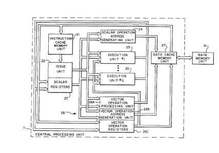
Figure 2 is an example of a central processing unit
of a data processing unit capable of using the present invention.
Figure 3 is an example of the technique for testing
array references according to the prior art.
Figure 4 illustrates the testing of array references
according to the present invention.
Figure 5A illustrates the information placed on the
data processing system stack in response to an exception condition
permitting identification of the exception producing condition.
Figure 5B is an illustrative format for the FLBC
instruction.
1~03745
Figure 6 illustrates the apparatus used to
identify the condition signal.
DESCRIPTION OF THE PREFERRED EMBODI~lENT
1. Detailed Description of the Figures
Referring now to Fig. lA and Fig. lB, two
exemplary data processing system configurations
capable of using the present invention are shown. In
Fig. lA, the central processing unit (#l) 11 is
coupled to a system bus 19. Other central processing
units (e.g., #N) 12 can also be coupled to the
system. The central processing unit(s) 11 (through
12) process data according to *he structure of the
central processing unit(s) in conjunction ~ith
central processing unit control programs, the control
programs being comprised of instructions resident in
the main memory unit 15. The nonresident data and
instructions are typically stored in the mass storage
unit(s) and are transferred to and from the main
memory unit 15 via the system bus 19. Input/output
unit(s) 1#1) 16 (through 1#~1) 17) couple devices such
as mass memory storage units, user terminal devices
and communication devices to t~e data processin~
system by means of the system b~s 19. The mass
storage units store the data and instructions
required by the data processing ~ni~(s). Sets of
data and/or instructions, typically designated as
pages of data and/or instructions. required for the
' ~303745
operation of the central processing units 11 through
12 are transferred from the mass storage units
having relatively slow accessibility to the main
memory unit to which access by the central processing
unit is relatively fast. The bus oriented system has
an advantage in the relative ease to reconfigure the
system but has the disadvantage that the each system
component requires control apparatus to provide an
interface with the system bus. Referring next to
Fig. lB a data processing system is shown in which
the central processing unit(s) 11 (through 12) and
the input/output unit(s) 16 (through 17) are coupled
to the main memory unit 15 through a memorv control
unit 14 the memory control unit 14 replacing the
system bus 19 and the control function performed by
individual data processing system components in the
bus oriented data processing configuration shown in
Fig. lA. The memory control unit 14 provides a
centralized control and monitoring of the transfer of
data and instructions that can be more efficient than
the bus oriented configuration of Fig. 1 but with
the loss of flexibility.
Referring next to Fig. 2 a block diagram of an
exemplary central processing unit capable of
effective utilization of the present invention is
illustrated. The issue unit 22 is responsible for
for providing (decoded) instructions to the plurality
~30374S
--7--
of specialiæed execution units comprising scalar
operation address generation unit 24, at least one
execution unit (#l) 25 (through execution unit (#Q)
26) snd a vec~or operation unit 28, the vector
operation unit 28 including vector operation
processing unit 28A, vector operation address
generation unit 28B and vector operation registers
28C. The data processed by the execution units are
typically extracted from the scalar registers 23 or
the vector registers 28C. The resulting data from
the execution units are stored in the scalar
registers 23, in the vector registers 28C or in the
data cache memory unit 27. The data cache memory
unit 27 csn be viewed as a cache memory unit
providing an interface between the main memory unit
15 and the central processing unit 11. (The data
cache memory unit 27 is shown as being coupled
directly to the main memory unit in Fig. 2. As
illustrated in Fig. lA and Fig. lB, the actual
coupling can include intervening data processing
apparatus.) The issue unit 22 includes apparatus for
determining which execution unit will process
selected data and for determining when the selected
execution unit is available for processing data.
This latter feature includes ascertaining that the
destination storage location will be available to
store the processed data. The instruction cache
~:~03745
--8--
memory unit 21 stores the instructions that are
decoded and forwarded to the appropriate execution
unit by the issue unit. The issue unit 22 has the
apparatus to attempt to maximize the processing
operations of the execution units. Thus, the issue
unit 22 includes prefetch apparatus and algorithms to
ensure that the appropriate instruction (including
any branch instruction) is available to the issue
unit 22 as needed. The plurality of execution units
are, as indicated by the scalar operation address
generation unit 24 and the vector operation unit 28,
specialized processing devices for handling certain
classes of processing operation. For example, an
execution unit can be configured to handle floating
point operations, or integer arithmetic operations,
etc. The issue unit 22 has associated therewith
scalar registers 23 that can store data required for
the execution of the program or for providing a
record of the data processing operation. For
example, one register is the Program Counter register
that stores the (virtual) address of the next
instruction, in the executing program instruction
sequence, to be processed. The scalar operation
address generation unit 24 is used to convert virtual
addresses to physical locations in the main memory
unit 15. The issue unit 22 is also responsible for
reordering the data from the execution units in the
130:~7AS
correct sequence when the execution units process
instructions at different rates.
Referring next to Fig. 3, the procedure for
testing for and responding to a Boolean condition,
according to the prior art, is illustrated in terms
of an invalid array index (address). In step 301, an
array index i5 calculated. In step 302, the
calculated array index is compared with the bounds
for all array indexes, and when the index is not
within the permissible bounds, the low bit position
of a specified register is cleared (i.e., a logic '0"
signal is stored therein. In step 303, the low bit
position of the specified register is tested to
determine if a logic '1' signal is stored therein.
h'hen a logic '1' signal is not stored therein (i.e.,
the low bit position is clear), a subroutine is
called to respond to the condition in step 304.
After the fault condition has been responded to, or
when the low bit position has a logic '1' signal
stored therein, then the program cantinues execution.
Referring to Fig. 4, the procedure for testing
and responding to the Boolean condition, according to
the present invention, is illustrated in terms of the
an array index checking routine (as in Fig. 3). In
step 401, the array index is calculated. In step
402, a comparison is made to determine if the index
is within the boundaries for array indexes and when
~303745
--10--
the index is not within the permissible bounds, a
logic '0' is stored in the low bit position of a
specified register. In step 403, the Fault on Low
Bit Clear (FLBC) instruction is executed. When the
low bit position of the specified register is clear
(i.e., has a logic '0' signal stored therein, then a
fault is signaled and a responsive subroutine is
executed in step 404. When the low bit position of
the specified register has logic '1' stored therein
in step 403 or at the conclusion of responsive
subroutine in step 404, the execution of the program
continues in step 405.
Referring next to Fig. 5A, when the fa~lt
condition is signaled, the data processing system
mechanism (e.g., implemented in apparatus or in a
special operating mode in the preferred embodiment)
responsive to the fault condition stores infor~ation
in the data processing unit stack that permits a
control program routine to localize the source of the
array reference error. In the preferred embodiment,
the faulting instruction 501 is stored in one field
(to preserve encoded information concerning the fault
that is included in the instruction itself in the
preferred embodiment), the processor status is stored
in field 502 and the virtual address of the fault on
low bit (clear) instruction is stored in field 503.
The processor status field includes status
:1303745
information such as interrupt level, vector
instruction enable signal, the vector restart frame,
the currently executing mode of operation signal and
a virtual machine monitor field.
Referring to Fig. 5B, an exemplary for~at for
the Fault on Low Bit Clear instruction is shown. In
field 510, the opcode field identifies (to the issue
unit 22) the instruction (for example, Fault on Low
Bit Clear) to be executed. In response, the issue
unit 22 activates the apparatus to execute the
instruction. Field 511 specifies to the issue unit
22 the register for which the Boolean condition (for
example, low bit clear) is to be examined. Field 512
provides information that permits the data processing
system to respond to the specific fault condition
signaled by the instruction, such as an address.
Referring to Fig. 6, the preferred embodiment
for an apparatus for detecting the condition signal
is illustrated. Associated with each scalar register
in the scalar register bank 230 of scalar register
unit 23 is a three bit summary register in register
bank 229 in issue unit 22. The three bits include a
bit position indicating that the associated register
in register bank 230 has all zeros stored therein.
The second bit position indicates the sign of the
data in the associated register. And the third bit
position is the same bit value stored in the least
1303~45
-12~
significant register position in the associated
register in register bank 230. A signal detection
unit 228 is provided so that any of the bit positions
of the associated summary register can be
interrogated. Thus, in response to an instruction,
such as Fault on Low Bit Clear, the signal in the
identified register can be identified and the fault
condition signaled when appropriate.
2. Operation of the Preferred Embodiment
The central processing unit having pipelined
execution units of Fig. 2 was implemented in the
preferred embodiment subject to several constraints,
however, other design implementations can utilize the
present invention. The central processing unit
includes a plurality of execution units, each
execution unit adapted to execute a class of
instructions. By way of example, one execution unit,
the scalar address generating unit 24, controls the
transfer of the logic signal groups between the
central processing unit and the main memory unit,
i.e., executes the scalar load/store instructions.
One execution unit is adapted to execute data
shifting operations, one execution unit for floating
point add/subtract operations, one execution unit is
adapted for integer and floating point multiply
operations and one execution unit is adapted for
integer and floating point divide operations. The
~3037AS
-13-
specialized execution units can be, but are not
necessarily implemented in a pipelined configuration.
The other features of the central processing unit are
the following. The instruction in the currently
executing sequence of instructions is transferred to
the issue unit 22 from the instruction cache memory
unit 21. In the issue unit, the instruction is
broken down into its constituent parts and
data-dependent control signals and address signals
are generated therefrom. However, before an
instruction can begin execution (i.e., be issued),
several constraints must be satisfiedO All source
and destination registers for the instruction must be
available9 i.e., no write operations to a needed
register can be outstanding. The regiseer write path
must be available at the future c~cle in which this
instruction will store the processed quantity. The
execution unit to be required for processing the
instruction during the execution must be available to
perform the operation. With respect to the vector
operation unit, a vector operation reserves an
execution unit for the duration of the vector
operation. When a memory load/store instruction
experiences a cache memory unit miss, the load/store
unit busy flag will cause the subsequent load/store
instructions to be delayed until the cache memory
miss response is complete. When an inseruction does
~30374S
-14-
issue, the destination register and the write path
cycle for the result are reserved. During operand
set-up, all instruction-independent register
addresses are generated, operands are read and
stored, and data-dependent control signals are
genPrated. The instruction operands and control
signals are passed to the associated execution unit
for execution. The result generated by the execution
unit is stored in the register files or in the data
cache memory unit 27 as appropriate. Once an
instruction issues, the result of the processing may
not be available for several machine cycles.
Meanwhile, in the next machine cycle, the next
instruction can be decoded and can be issued when the
requisite issue conditions are satisfied. Thus, the
instructions are decoded and issued in the normal
instruction sequence, but the results can be stored
in a different order because of the of the varying
instruction execution times of the execution units.
This out of order storing complicates the exception
handling and the retry of failing instructions.
l~owever, these events are relatively rare and the out
of order storing provides execution and hardware
advantages.
In comparing Fig. 3 and Fig. 4, the first two
steps 301 and 302 of Fig. 3 are the same as the first
two steps 401 and 402 of Fig. 4. In the prior art,
" ~3~13'745
--15-
step 303 required that a logical comparison be made
of the low bit position of the specified register and
a reference value. Such activity typically involves
a conditional branch around a subroutine call,
thereby disrupting the efficient sequential flow of
instruction execution. Conditional branch procedures
impose a large performance penalty on high
performance data processing systems. By comparison,
the FLBC instruction checks for the presence of a
fault condition, and the next sequential instruction
can be executed without delay when a fault condition
is not present. The presence of a fault condition
identified by this instruction causes the control
program to store information on the stack that will
permit the exception handling program to identify the
origin of a fault condition.
This type of instruction, i.e., the Fault on Low
Bit Clear instruction, can also be be used to chec~
the program execution status, when used in
conjunction with programming conventions. When a
program executes correctly, a Boolean value of true
(i.e., 'l') is returned, and a Boolean value of false
(i.e., '0') when an error is discovered. The error
status can be checked by a Fault on Low Bit Clear
instruction.
In the preferred embodiment, the execution units
separately provide the status signals (from step 403)
`` 1303745
-1`6-
to associated status or summary registers 229 at the
same time that the full quantities are being returned
to the scalar registers 23. The summary registers
permit more expeditious determination of the signal
stored in the specified position of the specified
register.
It will be clear to those skilled in the art
that, although the low bit position of the specified
register is used in the FLBC instruction, any
specified register position can be used to
communicate the condition information and can signal
a fault condition. It will also be clear that this
basic mechanism can be used to implement similar
functions, such as a Fault on Register Equal to Zero
condition or a Fault on Register Negative condition.
The foregoing description is included to
illustrate the operation of the preferred embodiment
- and is not meant to limit the scope of the invention.
The scope of the invention is to be limited onl) by
the following claims. From the foregoing
description, many variations will be apparent to
those skilled in the art that would yet be
encompassed by the spirit and scope of the invention.