Note: Descriptions are shown in the official language in which they were submitted.
1303754
BIPOI~R ~IOT ELE:CTRON TRANSISTOR
Field of the Invention
This application pertains to the field of active semiconductor devices.
In particular, it pertains to bipolar transistors in which at least a substantial fraction of the
5 current is carried by hot electrons.
Background of the Invention
It has been known for some time that a hot electron transistor could
potentially be operated at frequencies in excess of those achievable with conventional
(diffusive) transistors. See, for instance, T.E. Bell, IEEE Spectrum, February, 1986,
10 pp. 36-38. Various types of hot electron transistors (HET) have been proposed. This
application is concerned with one particular class of such transistors, namely,
heterojunction bipolar HETs. For a brief review, see L.F. Eastman, ibid, pp. 42-45.
The flow of electrons from emitter to collector in a bipolar transistor
is controlled by varying the emitter/base barrier potential by means of an applied voltage
15 V~, and is also a function of an externally applied voltage V~ between base and collector.
Under normal operating conditions, Vb, reverse biases the base/collector junction.
Electrons injected from the emitter into the base of a bipolar HET have energy
substantially greater than the thermal energy of the ambient electrons in the base. These
"hot" electrons ideally traverse the base without undergoing significant scattering. If the
20 base/collector barrier is caused to be lower than the hot electron energy then some of the
hot electrons can cross the barrier, be transmitted through the depletion region of the
collector, and enter the sea of conduction electrons in the collector contact region.
As will be readily understood by those skilled in the art, various
difficulties have to be overcome before a device of this type can function as a practical
25 HET. Among these is the difficulty of achieving substantially complete hot electron
transport through the base, and, desirably, also through the depletion region of the
collector.
.
~, .. .
1303754
1 a
Canadian Patent Application Serial No. 572,285 which was filed on
July 18, 1988, in the name of A. Levi, discloses means for achieving improved HETs.
However, in view of the general desirability of improved characteristics such as larger B
and high cut-off frequency, means for achieving further improvements in HET
5 characteristics would be of considerable
1303754
significance. This application discloses HETs comprising such means.
Definitions
Electron transport in a crystal is herein defined to be "ballistic" if, in addition to
its possible interaction with an accelerating electric field, the electron interacts substantially only
5 with the static part of the periodic lattice potential. Electron transport thus may be ballistic even
though the electrons undergo some small angle scattering and/or small energy change.
A conduction electron herein is considered to be a "hot" electron in a given
semiconductor region if its energy E is substantially greater than the ambient thermal energy kj3T.
Typically, E > lOkBT, where k~3 is the Boltzmann constant, and T is the absolute temperature of
10 the lattice.
A "hot electron" transistor (HET) is a transistor whose operative characteristics
are in substantial part determined by the transport of hot electrons through the transit region of
the transistor, with minimal scattering of the hot electrons in the transit region.
The "transit region" of a HET herein is that portion of the HET through which
lS substantial hot electron transport takes place, or is intended to take place. For instance, in a
bipolar transistor, the transit region consists of the base and the collector depletion region. In
order to have the possibility of significant hot electron transport in a HET, the width of the
transit region has to be less than the mean-free path of the hot electrons in the material.
The "ambient" charge carriers are those charge carriers (electrons or holes) that
20 are essentially in thermal equilibrium with the lattice. For instance, in n-p-n bipolar HETs the
ambient charge carriers in the base are holes.
Electron scattering is herein considered to be "elastic" or "inelastic" if the
associated change in energy of the electron is, respect*ely, less or greater than ~ = h/27~rbOb"
wherein _ is Planck's constant and rk,k, = m*,~/e, where m* is the effective hole mass, ,u is the
25 hole mobility, and e is the electron charge. (See, for instance, N.D. Mermin, Phvsical review B~
Vol. 1, pp. 2362-2363,1970.) Exemplarily, in GaAs with a p-type impurity concentration of
2xlO2cm3, ~ is about SO cm2/V-sec, yielding ~ of about 46 meV.
Summarv of the Inventioll
In accordance with one aspect of the invention there is provided a bipolar hot
30 electron transistor comprising a) an electron emission region (the first region), an electron
collection region (the third region), and a second region intermediate the first and third regions,
forming interfaces and being epitaxial therewith, the first, second, and third regions each
consisting of semiconductor material, with the composition of the second region material differing
..
`;
1303754
at least from that of the first region material at the first/second region interface, with at least a
part of each of the first and third regions having n-type conductivity, and with at least a part of
the second region having p-type conductivity, associated with the second region being a thickness
Zb~ a base resistance Rb, an average dopant density nb, and an inelastic scattering rate 1IT,~ for
S the hot electrons; b) means for making electrical contact with the first, second, and third regions,
respectively; and c) means adapted for causing injection of hot electrons of average energy E,
from the first into the second region, with at least a substantial portion of the injected hot
electrons crossing the interface between the second and third region; CHARA(,l I~.RIZED IN
THAT d) the inelastic scattering rate VT~n varies as a function of nb and has a ma~imum for a
10 given value of ~, with nb at the maximum to be referred to as nb",,~, and e) nb is selected to be
greater than nb""l, whereby the transistor can have a relatively small Zb and a relatively small base
resistance Rb-
Brief Descri~tion of the Dra~in s
FIG. 1 schematically depicts a device according to the invention;
FIG. 2 shows schematically some features of the conduction band structure of a
device according to the invention;
' \ '
. ~
~303754
FIGS. 3 and 4 show exemplary curves, respectively, of the inelasdc
and elasdc electron scattering rates in p-type GaAs as a funcdon of dopant
concentradon.
The Invention
In a broad sense, I am herein teaching design features that can be used
to produce HETs having improved characterisdcs. For instance, the inventive
features can result in compound serniconductor bipolar HETs that are capable of
operadon at frequencies higher than those attainable with prior art transistors.Such transistors can be used in a variety of applicadons, e.g., in repeaters in high
10 bit-rate opdcal fiber transmission systems.
HETs of interest herein generally have geometries similar to those of
prior art HETs, although typically cridcal dimensions such as Zb and Zc (see
FIG. 2) are scaled down. Invendve HETs comprise an electron emission region
(the firse region), an electron collecdon region (the third region), and a second
15 region that is intermediate the first and third regions and forms interfaces
therewith. The first region comprises an emitter layer, and the second region
comprises a base layer, with, typically, the emitter layer contacting the base layer
and forming the emitter/base in$erface therewith. The base layer is typically also
in contact with third region material and forms the base/collector interface
20 therewith. The first, second and third regions each generally consist of one or
more layers of compound semiconductor material, with the composition of the
base layer differing at least from that of the emitter layer. In many cases the
second region material will be basically the same as the third region material, with
the second and third region materials containing different dopants and/or differing
25 in dopant concentradon.
~ 3Ts of interest herein also comprise means for making electrical
contact with the first, second and third regions, respectively, and means for
injecting hot electrons from the first into the second region. At least a substantial
fraction (advantageously > 90%) of the injected hot electrons transit the second30 region without substantial energy loss and cross the base/collector interface. The
injected hot electrons have average energy Ei.
As will be readily appreciated by those skilled in the art, in a HET a
substantial portion of the hot electrons that are injected into the second region
mu$ traverse the second region and the remainder of the transit region without
35 becoming thermalized through inelastic scattering and, desirably, without
undergoing appreciable elastic or inelastic scattering. This suggests as a desirable
1303754
design goal transistors having relatively low dopant concentradon in the transitregion~ On the other hand, a high cut-off frequency can only be achieved if the
sheet resistance Rb associated with the application of a control signal to the
second region is relatively low. Low Rb requires a high dopant concentration in
5 the second region. Thus there exist conflicting requirements which have resulted
in design compromises in the prior art and prevented desirable scaling down of
device size.
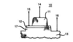
FIG. 1 schemadcally depicts a HET 10 according to the invention,
wherein numerals 11, 12, and 13 refer, respectively, to the first, second, and third
10 regions of the transistor. In many cases these regions can be directly identified
with emitter, base, and collector, respectdvely. Fach of the regions may comprise
more than one layer of serniconductor material. Portion 17 of the third region is a
collector depletion region, and numerals 14, 15, and 16 refer to means for making
electrical contact to the first, second, and third regions, respectively. Transistors
15 according to the invention may be discrete devices but are more likely part of an
integrated circuit, as will be appreciated by those skilled in the art. Discretetransistors as well as the integrated circuits can be produced by known methods,typically including molecular beam epitaxy (MBE) and/or metal-organic chemical
vapor deposition (MOCVD).
FI&. 2 schematically shows the energy diagram associated with an
exemplary inventive H~T under bias. Such diagrams are well understood by
those skilled in the art. The regions labeled "emitter", "base", and "collector"refer to the first, second, and third regions of the transistor, respectively, and
numerals 21 and 22 refer to the lower conduction band edge and the upper
25 valence band edge, respectively. The arrow indicates the direction of hot electron
flow, with nurneral 23 referring to the sea of conduction electrons in the ernitter
region, 24 to the holes in the valence band in the base region, and 25 to the sea of
conduction electrons in dle collector contact region. The base region is of
thickness Zb' and the collector depletion region of thickness Zc Zb and Zc
30 ~ogether are the thickness of the transit region, which is advantageously kept to a
minimum consistent with other design parameters such as Rb. EF h and EF e are,
respectively, the Ferrni energy of the holes in the base region and of the electrons
in the collector region. Vbc is the potential difference, due to an externally
applied voltage, between base and collector.
1303754
I have made a quite unexpected discovery which will permit the
practidoner to design HETs capable of improved high frequency behavior. As a
consequence of the newly discovered property, the above discussed conflicting
requirements on the doping of the second region are at least far less severe than
5 previously thought. In particular, I have discovered that the inelasdc scattering
rate l/~in associated with hot electrons of a given energy Ei in many
semiconductor materials of interest for HETs (e.g., GaAs, AlGaAs,
InO 53Gao 47As) goes through a maximum as a function of the average density of
dopant atoms (nb), and can be significantly lower than its value at nb max if
10 nb > nb max~ where nb max is the density of dopant atoms at the maximum of
l/~,r,. The inelastic scattering time is designated as ~,.
The inelastic scattering rate for hot electrons in p-doped GaAs is
shown in FIG. 3 as a function of dopant level. As can be seen, the scattering rate
is a function of E. for most dopant levels of interest and has a pronounced
15 maximum. For high doping levels (e.g., nb > 102cm~3) the inelasdc scatteringrate can actually be less than for low doping levels (e.g., nb < 1017cm~3).
Sirnilar results apply to other compound semiconductor materials useful in the
practice of the invendon. Thus, in devices according to the invendon the averagedopant concentradon in the base typically is at leas~ 102cm~3, frequendy
20 2xlO20cm~3 or greater.
As a consequence o~ the unexpected decrease of the inelasdc
scattering rate for high doping levels, it is possible to design HETs that have both
reladvely low Rb and low 1/~in, two characterisdcs that, up to now, pracddoners
did not expect to be obtainable simultaneously. This can be achieved by selecting
25 the doping level in the second region such that nb > nb max~ for the given
operadve value of Ei The value of nb max for a given semiconductor material
can be determined by a calculadon of the type used tO produce the results shown
in FIG. 3, or it can be determined experimentally, by carrying out UV
measurements at low temperatures on a series of otherwise identical BTs that
30 differ only with regard to nb.
It is to be understood ehat the above remarks pertain to the inelaseic
scaetering rate. The behavior of the elasdc scattering rate in GaAs as a funceion
of the level of randomly distributed p-type dopant is shown in FIG. 4. As can beseen from the figure, for dopant levels above about SxlO20cm~3 elasdc scattering35 from dopant ions is the dominant scattering mechanism for hot electrons in p-type
~303754
- 6 -
GaAs, if the ions are randomly distributed. Similar results obtain for the othersemiconductor materials referred to above.
In preferred embodiments of the invention the dopant atoms in the
second region are not randornly distributed, as has been customary up to now, but
5 are instead at least partially ordered, whereby the elastic scaKering Mte of the hot
electrons can be significantly reduced. An exemplary technique for attaining such
ordering in the direction parallel with the current flow is delta-doping (see, for
instance, E. F. Schubert et al, Physical Review B, Vol. 36 (1987) pp. 1348-1351),
whereby a spatially non-uniform distribution of dopant atoms is produced.
10 Typically such a distribution comprises one or more thin "sheets" of highly doped
material, the sheets being parallel to the en~itter/base interface. Another
exemplary technique for attaining ordering may comprise the formation of an
ordered alloy (see A. Gomyo et al, Physical Review Letters, Vol. 60(25) (1988),
pp. 2645-2648) in the second region. In this case the dopant atoms in the second15 region form part of the alloy's periodic laKice.
I have made a further discovery that can also contribute to improved
characteristics of HETs. In such devices, it is ~pically required that the hot
electrons that have transited the second region and have been transmitted through
the second/third region interface also be able to travel through the remainder of
20 the transit region (typically the collector depletion region) substandally without
scattering.
In many prior art HETs a significant scattering mechanism in (100)-
oriented III-V semiconductors is (intraband) intervalley scattering from the r tO
the X valley (those skilled in the art are familiar with this terminology). Electrons
25 typically are injected into the r valley in the second region, and it is advantageous
to keep the electrons in that valley throughout their traverse of the transit region.
The likelihood of r~x intervalley scattering in the transit region can be
signilicantly reduced if the average time the hot electrons spend in the part of the
transit region in which r~x scattering is less than the average scattering time for
30 r to X scattering (designated ~r-x) in the semiconductor material. The relevant
part of the transit region in which r~x scattering is possible depends on Vbc and
the thickness Zc. With the base/collector reverse biased to VbC=l volt the portion
of the third region in which r~x scattering can take place is about 0 79 Zc for
GaAs and about 0-33 Zc for In 53Ga 47As. Since ~r-x in many of the
35 semiconductors of interest herein can be estimated to be of the order of about
50 fs, in most III-V semiconductors of interest herein Zc desirably is less than
-
1303754
about 100 nm, in order to insure at least a relatively low r~x scattenng
probability in the transit region. For instance, if Zc < 50 nm in GaAs then little
r~x scattering takes place in the transit region for relevant values of Ei and Vbc;
for In 53GA 47As the same is true if Zc C 70 nm. Thus, in some preferred
S devices according to the invention the third region comprises an undoped or
relatively lightly doped por~on of thickness Z in contact with the second region,
and a reladvely highly doped pordon that is spaced apart from the second region,with Zc being at most about 100 nm.
In preferred HETs according to the invendon there are also limits on
10 VbC (see FIG. 2). To avoid interband scattering the electrons can be accelerated
in the third region only to an energy less than EbW, the energy width of the
conduction band in the third region. This implies that
e bc,max < Ebw ~ Eg ~ EF,e ~ EF,h~ where e is the electron charge, Vbc D3a7c is
the maximum allowed Vbc, Eg is the bandgap in the third region material, and
lS EF e and EF h are, respecdvely, the Fermi energy of the electrons in the contact
portion of the third region and of the holes in the second region. On the other
hand, in order to achieve short transit times and thus, potentially, high cut~fffrequencies, as well as high output impedance, it would be desirable to be able to
use relatdvely large Vbc. In preferred devices according to the invention, the
20 collector contact region is reladvely heavily doped, exemplarily containing more
than about 10l9cm~3, preferably more than 5xlOI9cm~3, dopant atoms.
In pardcularly preferred HETs according to the invendon the third
region comprises a material which has reladvely large EbW-Eg (reladve to GaAs,
which has EbW - 2.0 eV and Eg - 1.4 eV) since such devices can have a
25 relatdvely large operating voltage range of Vbc. Exemplarily, In 53Ga 47As is such a material.
In an exemplary embodiment of the invendon the emitter (11)
is n-type InP (Sxl017cm 3 dopant atoms, e.g., Si) and the base (12) and
collector (13) are In 53Ga 47As. The thickness of the base layer (Zb) is about
30 40 nm, and the thickness Zc of the collector depletion region (17) is about 70 nm.
The base consists, in sequence, of a S nm thick, essencially undoped, set-back
layer, followed by 6 ~doped sheets, vith 6 nm spacing between sheets, followed
by another S nm set-back layer. Each o-doped sheet contains lxl014cm~2 p-type
dopant atoms (e.g., Be~, resulting in an average dopant concentradon of
35 2xlO20crn 3 in the relevant pordon of the base layer. As will be appreciaced, a
1303754
- 8 -
o-doped layer is at most a few atomic layers thick. The thus produced spadally
non-uniform distribution of dopant atoms is expected to result in reduced elastic
scattering of the hot electrons, as opposed to prior art HETs with randomly
distributed dopant atoms in the base region. The n+ collector contact region is
5 about 300 nm thick, with a dopant density of Sxl019cm~3. The device is
produced by known techniques, exemplarily including MBE, lithography and
plasma etching. Electrical contacts (14, 15, 16) are made by a conventional
technique.
In a further exemplary embodiment of the invention a HET is made
10 substantially as described above, except that Al 35Ga 65As is used to form the
emitter layer, and GaAs is used for base and collector, with Zc being 50 nm. In
other embodiments the base layer contains 2 o-doped sheets of p-type dopant
atoms (areal density 3x1014cm~2~ instead of the previously described six. The
sheets are 30 nm apart, resulting in an average dopant density of 2xl02cm~3.
15 This doping scheme is expected also to result in reduced elastic scaKering.
The above referred to ~doping produces a non-random distribution in
the growth direcdon but normally would not result in ordering within the doped
sheets. At least partial ordering within the doped sheets is expected to be
obtainable by appropriate choice of deposition condi~ions. Such ordering is
20 expected to result in further reduction of elastic scattering of the hot electrons, and
therefore in irnproved device perforrnance.
Deposition condi2ions that are expected to result in at least partial in-
plane ordering are a relatively low substrate temperature (typically less than about
500-C) together with an overpressure (or underpressure) of an appropriate element
25 in the growth atmosphere. For instance, if Be is the dopant then overpressure (the
partial pressure typically being at least 150% of the normal partial pressure) of As
ensures that the Be atoms vill preferendally be located on Ga sites. On the odher
hand, if the dopant is C dhen an underpressure (dhe partia1 pressure typically being
at most 75% of dle normal partial pressure) of As, combined widl the deposition
30 of a fraction of a monolayer (e.g., about 1/2 monolayer) of Ga, ensures
preferential location of C on As sites. The low substrate temperature prevents
substantial surface diffusion of the deposited atoms, the procedure thus resulting
in partial ordering of dhe dopant atoms. Partial ordering is currendy considered to
result in substantial reduc~ion in 1/~,~1 if the Fourier transform of the distribution
35 function for dhe dopant atoms has a value of at most 0.1 in the range 0 S k S ki,
where ki is the average wave vector of the injected hot electrons. Ordering that
1303754
meets the above requirement will be referred to as "substantial" ordering. The
distribution function can, at least in principle, be determined by known techniques
such as scanning tunneling microscopy or electron diffraction.
"Partial ordering" in many herein relevant situations exists if the
S probability of finding a dopant atom on one type of lattice site (e.g., the Ga site in
GaAs) is substantially different from the probabili~ of finding such an atom on
the other type of lattice site (e.g., the As site in GaAs).