Note: Descriptions are shown in the official language in which they were submitted.
~3~3~
02 This invention relates in general to
03 marking devices, and more particularly to a low
04 profile inker for use within a semiconductor wafer
05 testing instrument.
~6 In the manufacture of integrated circult
07 chip wafers, there is a requirement for marking
08 defective circuits before the wafer is diced to
09 provide individual chips. Prior art marking devices
have been developed for ejecting drops of magnetic ink
11 on defective circuits of a wafer under test.
12 Examples of conventional prior art inker
13 systems can be found with reference to the IJ.S.
14 patents 3,943,527 ~Hartmann), 3,345,567 (Turner et
al), 3,185,927 (Margulis et al), 3,572,400 (Casner et
16 al) and 3,087,248 (Martin).
17 The conventional inkers of Turner et al,
18 Margulis et xl and Martin incorporate mechanical
19 apparatus for moving an inking element such as a pen
or fibrous wick into contact with the defective
21 circuit for marking the wafer. A disadvantage of such
22 mechanical systems is that physical contact be-tween
23 the inker and wafer circuits may result in advertent
24 damage of the wafer.
The prior art apparatus disclosed in the
26 Hartmann patent utilizes a "spritzer-type" inker in
27 which magnetic ink is forced onto a defective circuit
28 through a needle by means of a solenoid activated
29 plunger connected on top of and in line with a
reservoir for storing magnetic ink.
31 A disadvantage of prior art inkers such as
32 Hartmann is that the height of such inkers typically
33 interferes with passage of the pro~e test head which
34 is disposed above the inker. The height of the inker
is a direct result of the in-line connection of the
36 solenoid activated plunger to the reservoir filament
37 and the resulting linear axis movement effected
38 therebetween. In other words, the overall length of
~;~U3~
01 - 2 -
02 the inker from the tip of the needle to the top of the
03 plunger is typically in the vicinity of 8 centimeters,
04 with the top-most portion of the plunger interferring
05 with movement of the probe test head.
06 Thus, in order to move the test head
07 according to prior art inkers such as Hartmann, the
08 inker is required to be manually moved. Movement of
09 the inker may result in a number of disadvantages such
as high risk of probe card damage, difficult handling
11 of the inker from the undersurface of the probe test
12 head, and unsteady installation of the inker.
13 Furthermore, it has been found that excess ~ime is
14 required to move the inker in order to install a new
socket adaptor for testing.
16 There has been an industry bias towards
17 in-line connection of the solenoid plunger and inker
18 reservoir for the principle reason that linear axis
19 movement of the solenoid plunger and inker Eilament i5
inherently easy to adjust for eliminating binding of
21 the inker filament within the reservoir in the event
22 of off-axis inclination of the plunger arm and inker
23 filament.
24 In an effort to overcome the excess height
disadvantage of prior art in-line inkers such as
26 Hartmann, some manufacturers have produced in-line
27 solenoid plunger actuated inkers which are connected
28 to the testing apparatus at an oblique angle, and
29 utilize a curved inker needle extending from the
reservoir to the wafer under test at an angle of
31 approximately 80. An example of such a prior art
32 inker system is the model B-100-LTX inker manufactured
33 by Xandex of Petaluma, California. A significant
34 disadvantage of prior art inkers utilizing curved
inker needles is that the advantage of gravity feed is
36 lost over the vertically oriented in-line systems,
37 which places much greater reliance on relatively low
38 efficiency capillary action within the inker.
~3~i3~
01 - 3 -
02 According to the present invention, an
03 inker is provided wherein the solenoid actuated
04 plunger is disposed in parallel with the ink reservoir
05 on a main support arm and is connected to the inker
06 filament by means of a parallel activator or angle
07 pin. The parallel activator translates ver-tical
08 movement of the solenoid plunger into parallel
09 movement of the inker filament for forcing liquid from
the reservoir onto the semiconductor wafer under
11 test. By positioning the solenoid plunger beside and
12 in parallel with a reservoir, the overall height of
13 the inker is reduced substantially (eg. typically on
14 the order of 2.5 centimeters) thereby removing the
traditional obstruction to passage of the probe test
16 head as exemplified by the above discussed prior art.
17 In general, according to the present
18 invention, there is provided a low profile inker for
19 use in a probe instrument provided with a movable
probe test head for testing circuits on a
21 semiconductor wafer and in response generating control
22 signals indicative o~ defective ones of the circuits.
23 The inker is comprised of a support arm connected to
24 the probe instrument beneath the test head; an inker
reservoir mounted on the support arm for storing a
26 quantity of marking liquid, including a substantially
27 vertical inker filament for forcing the liquid from
28 the reservoir; a solenoid operated plunger mounted on
29 the support arm parallel to the reservoir, for
receiving the control signals and in response moving
31 in a substantially vertical axis; a needle extending
32 substantially vertically downward from the reservoir
33 for directing the liquid forced from the reservoir
34 onto the defective circuits; and a parallel activator
connecting the plunger and the inker filament for
36 translating vertical movement o~ the plunger into
37 parallel movement of the inker,
.
~?3~Q~
01 - 4 -
02 filament thereby forcing the liquid onto the defective
03 circuits, whereby parallel mounting of the plunger and
04 reservoir on the support arm contributes to a low
05 overall height of the inker sufficient to allow free
06 passage of the movable test head over the inker.
07 A better understanding of the present
08 invention will be obtained with reference to the
09 detailed description below in conjunction with the
following drawings, in which:
11 Figure 1 is a side view of a prior art
~2 inker for use in a semiconductor testing instrument;
13 Figure 2 is a side view of an inker in
14 accordance with the present invention;
Figure 3 is a detailed side view of the
16 inker in accordance with a preferred embodiment of the
17 present invention; and
18 Figure 4 is a front view of the inker
1~ shown in Figure 3.
Turning to Figure 1, a prior art inker is
21 shown comprised of a reservoir 1 for storing marking
22 liquid such as magnetic ink, and a solenoid activated
23 plunger 2 mounted in line with the reservoir 1, the
24 reservoir and plunger both being mounted on a main
support 3. The inker is connected via an additional
26 support ~ to the main body of the semiconductor
27 testing instrument, otherwise known as a prober.
28 The testing instrument is typically any of
29 a number of well known semiconductor tes~ers such as
those manufactured by LTX, Fairchild or Megatest,
31 etc. The testing instrument is further comprised
32 typically of a chuck for holding a wafer under test
33 (not shown) disposed directly beneath the tip of a
3~ needle 5 extending from the reservoir 1 of the inker.
One or more probes 6 assembled on a probe card
36 7 contact the wafer circuit under test for detecting
37 defects, etc, by applying predetermined control test
38 signals thereto. A ring adapter 8 houses the
~3~'3~
01 - 5 -
02 probe card 7 and is attached to a plate 9 which in
03 turn is connected to portions of the interfacing
04 instrument denoted as the ring lOa, and the ~uzz
05 button ring lOb.
06 The probe test head typically contains
07 microprocessor intelligence for generating test
08 current to the probe leads 6 through the rings (i.e.
09 fuzz button ring lOb) which includes usually 60 metal
spring pi~ conductors. The wafer i5 supported beneath
11 the probes 6 on the chuck (not shown) and moved into
12 various positions under control of the testing
13 instrument which also generates signals for energizing
14 the inker solenoid 2, in a well known manner. The
operation of the probe test head in conjunction with
16 the inker is described in detail with reference to the
17 aforementioned U.S, patent of Hartmann.
18 As shown in Figure 1, the in-line
19 arrangement of solenoid plunge~ 2 with inker reservoir
1 re~ult~ in an obstruction to passage of the test
21 head over the fuzz button ring lOb.
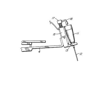
22 Turning to Figures 2-4, an inker is shown
23 constructed in accordance with the present invention
24 comprised of a reservoir 11 mounted on a main support
13 in parallel with a solenoid 15 housing a plunger
26 arm 17. A parallel activator 18 is threaded into
27 plunger arm 17 for connecting the plunger arm to an
28 inker filament within the reservoir 11.
29 According to the present invention, the
solenoid 15 is installed in parallel with the inker
31 reservoir 11 instead of being on the same axis as in
32 the prior art system of Figure 1. In the successful
33 prototype of the present invention, parallel
34 disposition of the solenoid with respect to the
reservoir resulted in a decrease in overall height of
36 the inker by 2.5 centimeters, which was found to be
37 sufficient for allowing passag~ of the test head over
38 the fuzz button ring lOb of the testing instrument.
39 According to the prior ark inker of Figure
'
1;1~?3~p~
01 - 6 -
02 1, the support 3 was characterized by a total len~th
03 or height of approximately 5 centimeters which was
04 reduced according to the successful prototype of the
05 present invention as illustrated in Fi~ure 2, to a
06 length of 3 centimeters, for facilitating passage of
07 the test head over the fuzz button ring.
08 As shown with reference to Figure 3, a
09 bracket 14 is shown connected to main support 13 for
supporting the solenoid 15 using two metal bolts 20
11 inserted through the support 13 and end plate 21. The ,
12 plate 21 also serves as a support for the attachment
13 4 (Figure 2) holding the main support 13 to the test
14 instrument.
The parallel activator 18 is preferably in
16 the form of an angle pin o~ approximately 10
17 millimeters in length which is screwed into the
18 solenoid plunger 17.
19 In operation, the test instrument
generates a control signal carried by solenoid leads
21 22, for energizing solenoid 15 which in turn causes
22 plunge~ 17 to be pulled within the solenoid against
23 the force of coiled spring 16. The parallel activator
24 or angle pin 18 translates vertical movement of the
plunger 17 within solenoid 15 into parallel movement
26 of the inker filament within reservoir 11. This
27 effectively forces the marking liquid from the
28 reservoir 11 via needle 12 onto the semiconductor
2~ wafer circuit under test.
The needle 12 and activator 23 form part
3] of the reservoir 1. The activator is preferably a
32 plastic pin attached to a plastic inker filament (not
33 shown) within the reservoir. The activator 23 is
34 attached to the metal angle pin 18 by means of a ball
and socket joint 19, wherein the angle pin 18 has a
36 filed head forming a bulbous portion.
37 The concept of parallel activation of the
38 inker filament by means of angle pin 18 is believed to
~l3~3~
Jl - 7 -
02 be a significant departure from the axial activation
03 of prior art systems such as shown in Figure 1.
04 One of the industry biases towards axial
05 activation of the inker Eilament, and away from the
06 parallel activation of the present invention, is that
07 the probe or test instrument attachment 4 is required
08 to be securely connected to main support 3 (Figure
09 1). The attachment of the support 4 to the main
support 3 in prior art systems was characterized by a
11 required length of typically 33 millimeters for
12 securely holding the inker to the support 4.
13 According to the present invention, the
14 metal plate 21 serves as a support for the attachment
4 and the solenoid 15, such that the overall length of
16 the attachment 4 may be reduced to approximately 12
17 millimeters.
18 As discussed above, the angle pin 18 must
19 be adjusted to a correct length within the plunger 17
in order that movement of the activator is directly in
21 line with the center axis of the reservoir 1 in order
22 for preventing the activator from binding and becoming
23 stuck within the reservoir.
24 Thus, an industry bias has developed
toward the simple adjustment of the inker filament in
26 relation to the movement of the plunger arm as
27 provided by prior art axial movement systems.
28 According to the present invention, adjustment of the
29 angle pin 18 is effected by simply screwing the pin 18
into small threads within the plunger 17, as shown in
31 Figures 3 and 4.
32 A person understanding the present
33 invention may conceive o~ other variations or
34 modifications therein. All such variations and
modifications ar~ believed to be within the sphere and
36 scope of the present invention as defined by the
37 claims appended hereto.