Note: Descriptions are shown in the official language in which they were submitted.
?3~3
IMPROVED BARRIER LAYER AND ORIFICE PLATE FOR THERMAL
INK JET PRINT HEAD ASSEMBLY AND METHOD OF MANUFACTURE
Technical Field
This invention relates generally to ~hermal ink
10jet printing and more particularly to an ink jet print head
barrier lay~r an~ orifice plate o~ improved geometry for
extending the print head lifetime. This invention is also
directed to a-novel method o~ fabricating this barrier layer
and orifice plate.
Back~round Art
In the art of thermal ink jet printing, it is
known to provide controlled and localized heat transfer to a
defined volume of ink which i~ located adjacent to an ink
2~ jet orifice. This heat transfer is sufficen~ to vaporize
the ink in such volume and causa it to expand, thereby
ejecting ink from the orifice during the printins of charac~
ters on a print medium. The above predefined volume of ink
is customarily provided in a so-called barrier layer which
is constructed ~o have a plurality of ink reservoirs
therein. These reservoirs are located between a
corresponding plurality of heater resistor elements and a
corresponding plurality of orifice segments for ejecting ink
30 therefrom.
one purpose of these reservoirs is to contain the
expanding ink bubble and pressure wave and make ink ejection
more efficient. Addi~ionally, the reservoir wall is used ~o
slow down cavita~ion produced by tha collapsing ink bubble.
35 For a further discussion of this pressure wave phenom~na,
reference may be made to a book by F. G. Hammltt entitled
Cavita~ion and Multiphase FlQw_Phenomena, ~cGraw Hill 1980,
page 167 et seq,
The useful li~e of these prior art ink jet print
head assemblies has been limited by the cavitation-produced
B
~l3~3~
wear from the pressure wave created in the assembly when an
ink bubble collapse~ upon ejec~ion from an orifice. This
5 pressure wave produces a significant and repeated force at
the individual heater resistor elemants and thus produces
wear and ultimate failure of one or more of these resistor
elPments after a repeated number of ink jet operations. In
addition to the above problem of resistor wear and failure,
10 prior art ink jet head assemblies of the above type have
been constructed using polymer materials, such as those
known in the art by the trade names RISTON and VACREL. .CP4
Whereas these polymer materials have proven satisfactory in
many respects, they have on occasion exhibited unacceptably
15 high failure rates when subjected to substantial wear pro-
duced by pressure waves from the collapsing ink bubbles
during ink jet printing operations. Additionally, in some
printing applications wherein the printer is exposed to
extreme environments and/or wear, these polymer materials
20 have been known to swell and lift from the underlying sub-
strate support and thereby render the print head assembly
inoperative.
~isclosure of Invention
The general purpose of this invention is to
increase the useful lifetime of these types o~ ink jet printhead assemblies. This purpose is accomplished by redu~ing
the intensity of the pressure wave created by collapsing ink
3 bubbles, while ~imultaneously improving the structural inte
grity of the barrier layer and orifice plate and strength of
materials comprising aame. Additionally, the novel smoothly
contoured geometry of the exit orific2 increases the maximum
achievable frequency of operation, fmax.
The reduction in pressure wave intensity, the
increase in barrier layer strength and integrity, and the
increase of fmax are provided by a novel barrier layer and
orifice plate geometry which includes a discontinuous layer
of metal having a plurality of distinct sections. These
sections are con~oured to de~ine a corresponding plurality
of central cavity region~ which are axially aligned with
.
.
.
.
.. , : .
3~3
, -
respect to the direction of ink flow e~ected ~rom a print
head assembly. Each of these c~ntral cavity regions connect
5 with a pair of constricted ink flow ports having a width
dimension substantially smaller than the diameter of the
central cavity regions. In addition, these sections have
outer walls of a scalloped configuration which serve to
reduce the reflective acoustic waves in the assembly, to
oreduce cros~-talk between adjacent orifice~, and to thereby
increase the maximum operating frequency and the quality of
print produced.
A continuous layer of metal adjoins the layer of
discontinuous metal sections and includes a plurality of
15output orifices which are axially aligned with the cavities
in the discontinous metal layer. These orifices have diame-
ters smaller than the diameters of the cavities in the
discontinuous layer and ~urther include contoured walls
which defin~ a convergent output orifice and which extend to
20 the psripheries o~ the cavities. Th~s convergent output
orifice geometry serves to reduce air "gulping" which inter-
fers with the continuou~ smooth operation of the ink jet
printhead. Gulping i5 the phenomenon of induced air bubbles
during the process of bubble collapsing.
By li~iting thQ width of the ink ~low ports
extending ~ro~ the cavit~e~ defined by the discontinuous
metal layer, the resistance to pr~s~ure wave forces within
the assembly is increasod. This feature reduces and mini-
30 mizes the a~ount of "gulping" and cavitation (and thuscavitation producQd wear) upon th~ individual heater resis-
tor alement~ in the assembly. Additionally, the limited
width of the~e ink flow ports ~erve~ to increa~e the effi-
ciency of ink e~ection and li~its the r~fiil~time for khe
35 ink reservoir~, further reducing cavitation damage.
Furthermor~, by using a layered nickel barrier structure
instead of polymer materials, the overall streng~h and inte-
grity of the print head assembly i~ suhstantia~l~ increased.
Accordingly, it is an object of an aspect of the
present invention to increase the lifetime of thermal ink
jet print head assemblied by reducing cavitation-produced wear on the
~3~3~''3
individual resistive heater elements therein.
An object of an aspect of the invention is to
increase the lifetime of such assemblies by increasing
the strength and integrity of the barrier layer and
orifice plate portion of the ink jet print head
assembly.
An object of an aspect of the invention is to
increase the maximum achievable operating frequency,
fmax~ f the inX jet print head assembly.
A feature of an aspect of this invention is the
provision of a smoothly contoured wall extending between
the individual ink reservoirs in the barrier layer and
the output exit orifices of the orifice plate. This
contoured wall defines a convergent orifice opening and
serves to reduce the rate of ink bubble collapse and
reduce the interference with the next succeeding ink jet
operation.
A feature of an aspect of this invention is the
provision of a economical and reliable fabrication
process used in construction of the nickel barrier layer
and orifice plate assembly which required a relatively
small number of individual processing steps.
A feature of an aspect of this invention is the
precise control of barrier layer and orifice plate
thickness by use of the electroforming process described
herein.
Various aspects of this invention are as follows:
In a thermal ink jet print head assembly including
a plurality of resistive heater elements located on a
thin film resistor structure and urther having a plur-
ality of individual ink reservoirs constructed atop the
plurality of resistive heater elements, respectively,
for receiving thermal energy therefrom during an ink jet
printing operation, the improvement comprisingo a
barrier layer and orifice layer structure and geometry
including a discontinuous layer of metal having a
B
~L3~3~3
4a
plurality of interrupted sections therein defining a
corresponding plurality of cavity regions axially
aligned with said heater elemPnts and with respect to
the direction of ink flow; each of said cavity regions
being connected to constricted ink flow ports having
widths substantially smaller than the diameters of said
cavities, and a continuous layer of metal joining said
discontinuous layer and having a plurality of output
orifices axially aligned with said cavities and having
output openings smaller than the diameters of said
cavities; said output orifices further including smooth
contoured walls extending from the peripheries of said
cavities to said output openings and operative to
minimize the turbulance of ink flow through said
cavities and exiting said output orifices and thereby
increasing the maximum achievable frequency of
operation.
A process for fabricating a barrier layer and
orifice plate structure for a thermal ink jet printhead
comprising:
a. forming a mask of a predetermined limited thickness
on a selected metallic substrate;
b. electroforming a first layer of metal on said
substrate and extending in a contoured surface
geometry into contact with said mask and defining
an ori~ice output opening;
c. forming a second mask atop said first mask and
thicker than said first mask, and having vertical
walls extending above the surfare of said first
layer of metal;
d. electroforming a second layer of metal on said
first layer and adjacent said vertical walls of
said second mask so as to define an ink reservoir
cavity bounded by vertical walls ext~nding from
edges of said contoured surface geometry of said
first metal layer; and
B
3~ 3 ~,h3
4b
e. removing said first and second masks and said
selected metallic substrate, thereby leaving intact
said first and second metal layers in a composite
layered configuration where said vertical walls of
said second layer define boundaries of ink
reservoirs of said structure.
The process for forming an integrated orifice plate
and barrier layer structure which includes the steps of:
a. forming a first mask portion having a convergently
contoured external surface and a second mask
poxtion having straight vertical walls, and
b. electroforming a first metal layer around said
first mask portion to define an orifice plate layer
having one or more convergent orifices, and -
electroforming a second metal layer around said
second mask portion to define a barrier layer
having one or more ink reservoir cavities aligned
respectively with one or more of said convergent
orifices in said orifice plate layer.
These and other objects and features of this
invention will become more readily apparent in the
following description of the accompanying drawings.
Brief Description of Drawinqs
Figures lA through lH are schematic cross-sectional
diagrams illustrating the sequence of process steps used
in the fabrication of the barrier layer and orifice
plate assembly according to the invention.
Figure 2 is an isometric view of the barrier layer
and orifice plate assembly of the invention, including0 two adjacent ink reservoir cavities and exit orifices.
Figure 3 is a sectional isometric view illustrating
how the barrier layer and orifice plate assembly is
mounted on a thin-film resistor structur~ of a
~3~t3~3~
thermal ink jet print head assembly.
Best Mode For CarrYin~ Out The Invention
Referring now to Figure 1, there is shown in
Figure lA a stainless steel substrate 10 which is typically
30 to 60 mils in thickness and has been polished on the
upper surface thereof in preparation ~or the deposition of a
positive photoresist layer 12 as ~hown in Figure lB. The
positive photoresist layer 12 is treated using a conven-
tional masking, etching and relat~d photolithographic
processing steps known to those skilled in the art in order
to form a photoresist mask 14 as shown in Figure lCo Us.ing
a positive photoresist and conventional photolitography, the
mask portion 14 i~ exposed to ultraviolet light and there-
upon is polymerized to remain intact on the sur.Eace of ~he
stainless steel substrate 10 as shown in Figure lC. The
remaining unexposed portion~ of the photoresist layer 12 are
developed using a conventional photoresi~t chemical
developer.
Next, the structure of Figure lC is transferred to
an electroforming metal deposition station where a fixst,
continuous layer 16 of nickel is deposited as shown in
Figure lD and forms smoothly contoured walls 18 which pro-
ject downwardly toward what eventually becomes the output
orifice 19 of the ori~ice plate. This contour 18 is
achieved by the ~act that the electroform~d first nickel
layer 16 overlaps the outer edges of the photoresist mask
14, and this occurs because there will be some electro-
forming reaction through the outer edge~ of the photoresist
mask 14. This occurs due to the small 3 micron thickness of
th~ photoresist mask 14 and ~he ~act tha~ the elect~oforming
process will penetrate the thin ma~k 14 at least around its
outer edge and ~orm the convergent contour as shown.
Electro~orming is more commonly known as an adap-
tation of electroplating. The electroplating is
accomplished by placing the part to be plated in a tank (not
shown) that contains ~he plating solution and an anode. The
plating solution contain~ ions o2 the metal to be plated on
3~(~3
the part and the anode is a piece of that same metal. The
part being plated i~ called the cathode. Direct current is
5 then applied between the anode and cathode, which causes the
metal ions in the solution to move toward the cathode and
deposit on it. The anode dissolves at the same rate that
the metal is being deposited on the cathode. This system
(also not shown) is called an electroplating cell.
At the anode, the metal atoms lose electrons and
go into the plating solution as ca~ions. At the cathode,
the reverse happens, the metal ions in the plating solution
pick up electrons from the cathode and deposit themselves
there as a metallic coating. The chemical reactions at the
15 anode and cathode, where M represents the metal being
plated, are:
Anode: M M+ + e
Cathode: M+ + e M
Electroforming is similar to electroplating, but
in the electroforming process an object is electroplated
with a metal, but the plating is then separated from the
object. The plating itself is the finished product and in
most case6, the object, or substxate 10 in the present
process, can be reused many times. As will be seen in the
following description, the removed plating retains the basic
shape of the substra~e surface and masks thereon.
In the next step shown in Figure lE, a thick layer
of laminated photoresist 20, typically 3 mils in thickness,
is deposited on the upper surfac~ of the first layer 16 of
nickel and therea~ter the coated structure is transferred to
a photolithographic masking and developing sta~ion where a
35 second photoresist mask 22 is formed as shown on top of the
first photoresist mask 14 and covers the contoured wall
section 18 of the first stainless steel layer 16. This
second photoresist mask 22 includes ver~ical side walls 24
of substantial vertical thickne~s, and these steep walls
prevent any electroforming beyond ~hese vertical boundaries
in the next electro~orming step illu~trated in Figure lG.
... .
~3~ 3
In the second plating or eleotroforming step shown
in Figure lG, a second, discontinuous layer 26 of nickel is
5 formed as shown on the upper surface of the first nickeel
layer 16, and the first and second layers 16 and 26 of
nickel are approximately a combined thickness of 4 mils.
The thickness of layer 16 will be about .00~5 inches and ~he
thickness of layer 26 will be about .0015 to .0020 inches.
loThe second photoresist mask 22 is shaped to provide the
resultant discontinuous and scalloped layer geometry shown
in Figure lH, including the arcuate cavity walls 31 and 33
extending as shown between ~he ink flow ports 35 and 37
respectively. The scalloped wall portions 30 o~ the dis-
15 continuous second layer of metal 26 serve to reduce acousticreflective waves and thus reduce cross-talk between adjacent
orifices 32.
A significant advantaga of using the above elec-
troforming process lies in the fact that the nickel layer20 thickness may be carefully controlled to any desired
measure. This feature is in contrast to the use of VACREL
and RISTON polymers which are currently available ~rom cer-
tain vendors in only selectively spaced thicknesses.
onc~ the barrier layer and orifice plate-composite
25 structure 28 is completed as shown in Figure lG, the struc-
ture of Figure lG iq tran~ferred to a chemical stripping
station where the structure is imoersed in a suitable photo-
resi~t stripper which will remove both the first and second
30 photoresist masks 22 and 24, carrying with them the stain-
less steel subs~rate 10. Advantageously this substrate 10
has been used as a carrier or "handle" throughout the first
and second electro~orming step~ described above and may be
reused in sub~equent electrofo~ming processes. Thus, the
35 completed barrier layer and orifice plate assembly 28 is now
ready for transfer to a gold plating bath where it is
immersed in the bath for a time of approximately one minute
in order to form a thin coating of gold over the nickel
surface of about 20 micrometers in thickness.
This gold plating step per se i5 known in the art
and is advantageously used to pro~ide an inert coating to
~a3~3~
prevent corrosion from the ink and also to provide an excel-
lent bonding material for the subsequent ~hermosonic (heat
5 and ultrasonic energy) bonding to solder pads ~ormed on the
underlying and supporting thin film resistor substrate.
Thus, the fact that the metal orifice plate and barrier
layer may be gold plated to produce an inert coating thereon
makes this structure highly compatible with the soldering
lOprocess which is subsequently used to bond the barrier layer
to the underlying passivation top layer of the thin film
resistor substrate. That is, nickle which has not been gold
plated is subject to surface oxidation which prevents the
making of good strong solder bondq. Also, the use o~ poly~
15 mer barrier materials of the prior art prevents the gold
plating thereof and renders it incompatible ~ith solder
bonding.
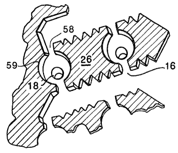
Referring now to Figure 2, ther~ i5 shown an
isometric view looking upward through the exit ori~ice~ of
20 the composite barrier layer and orifice plate assembly 28.
The contoured walls 18 ~xtend ~etween the output orifice
opening and the second nickel layer 26 and serve to increase
the maximum achievable operating frequency, fmax~ of the ink
jet print head when compared to prior art ~arrier plate
25 configurations having no such contour. In addition, this
nickle-nickle barrier layer and orifice plate and geometry
thereof serves to prevent gulping, to reduce cavitakion, and
to facilitate high yield manufacturing with excellent solder
30 bonding properties as previously dasired.
The width of the constricted ink flow port 58 will
be approximately .0015 inche~, or about one-half or less
than the diameter of ink reservoir 59. This diamet~r will
typically range from .003 to .005 inches. The diameter of
35 the outpu~ ink ejection orifice 32 will be about .0025
inches.
Referring now to Figure 3, the composite barrier
layer and oriPice plate 28 is m~unted atop a thin film
resistor struc~ure 33 which includes an underlying silicon
sub~trate 40 typically 20 mils in thickness and having a
thin sur~ace passivation layer 42 of silicon dioxide
~3U3~
thereon. A layer of electrically resistiYe material 44 is
deposited on the surface of the SiO2 layer 42, and this
5 resistive material will typically be tantalum-aluminum or
tantalum nitride. Next, using known metal conductor deposi-
tion and masking techniques, a conduc~ive pa~tern 46 o~
aluminum is formed as shown on top of the resis~ive layer 44
and includes, for example, a pair of openings 47 and 49
lO therein which in turn defin~ a pair of electrically active
resistive heater elements (resistors) indicated as 50 and 52
in Figure 3.
An upper surface passivation layer 53 is provided
atop the conductive trace pattern 46 and is preferably a
15 highly inert ma~erial such as silicon carbide, SiC, or
silicon nitride, Si3N4, and thereby serv~s to provide good
physical isolation between the heater resistors 50 and 52
and the ink located in the reservoixs above th~se resistors.
Next, a layer (or pads) 55 of solder is disposed
20 between the top surface of the passivation layer 53 and the
bottom surface of th~ nickel barrier layer 26, and as
previously indicated provides an excellent bond to the gold
plated sur~aces of the underlying pa~sivation layer 53 and
the overlying nickle barrier layer 26.
As i well known in the art of thermal ink jet
printing, electrical pul~e3 applied to the aluminum conduc-
tor 46 will provide resistance haating of the heater
elements 50 and 5~ and thus provid~ a trans~er of thermal
30 en~rgy from the~e heater elements 50 a~d 52 through the
sur~ace pa~sivation l~yer 53 and to the ink in the reser-
voirs in the nickel layer 26.
The silicon sub~trate 40 i5 bonded to a manifold
header tnot shown) u~ing conventional silicon-die bonding
35 techniques known in the art. Advantageously, thi~ header
may be of a chosen pla~tic matarial which is preformed to
receive the conductive leads 46 which have been previously
stamped from a lead frame ~also not shown~. This lead frame
is known in the art as a tape automated bond (TAB) flexible
circuit of the type disclosed in U.S. Patent l~o. 4, 635, 073,
issued January 6, ]987, Gary Hanson and assigned to the
~l3~3~ 3
present assignee.
In operation, heat is transmitted through the
5 passivation layer 53 and provides rapid heating of the ink
sto~ed within the cavities of the barrier layer and orifice
plate structure 28. When this happens, the ink stored in
these cavities is rapidly heated to boiling and expands
through the exit orifices 32. However, when the expandin~
10 ink bubble subsequently collapses during cavitation at the
ink jet orifices 32, the contour of the convergent output
orifices and the reduced width of the constricted ink flow
ports 58 serve to slow down the collapse of the ink bubble
and thereby reduce cavitation intensity and the damage
15 caused thereby. This latter feature results in a signifi-
cant resistance to this cavitation-produced downward pres-
sure toward the resistive heater elements 50 and 52.
Thus, there has been described a novel barrier
layer and orifice plate assembly for thermal ink jet print
20 heads and a novel manufacturing process therefor. Various
modifications may be made to these above described embodi-
ments of the invention without departing from the scope of
the appended claims.