Note: Descriptions are shown in the official language in which they were submitted.
-1- RCA 85,111
SYSTEM FOR ADAPTIVELY GENERATING SIGNAL IN ALTERNATE
FORMATS AS FOR AN EDTV SYSTEM
This invention relates to a system for changing
the form of a signal to be ~ransmitted, responsive to a
feature o~ the signal.
BACKGROUND OF THE INVENTION
The invention will be described in the
environment of an enhanced definition television (EDTV)
system, however it is not to be construed as limited to
this application.
The television industry is striving to improve
the ~uality of displayed television images. To thi~ end
several EDTV and hi~h definition television (HDTV) systems
have been proposed. The EDTV systems develop broadcast
signals which are compatible for reception by existing
standard receivers, but contain auxiliary signal components
which may be utilized by EDTV receivers to generate
enhanced images. The HDTV system~ generate broadcast
signals for producing high resolution, wide aspect ratio
images on HDTV receiver~, which signals are not compatible
for reception by current day "standard" receivers. In both
the EDTV and HDTV systems, in general it is necessary,
either for regulatory reasons or pragmatic reasons to
encode th~ original source image signals in a freguency
spectrum of bandwidth narrower kha~ the bandwidth of the
source signals. Typically the encoding formats are
established according to some stati~tically avexage signal
feature whereby for the majority of transmitted images the
respective receiver will be capable of faithfully
reproducing the original image. ~owever for certain
images, for example the bandwidth of a particular ncoded
signal component may be insufficient and result i~ a poorer
quality reproduced i~age. As an example consider the EDTV
system described by Isnardi et al., entitled "Decoding
Issues In the ACTV System", IEEE Transactions on Consumer
Electronics, Vol~. 34, No. 1, February I98~, pp. 111-120,
-2- RCA ~5,111
also described ;n U. S. Patent 5,025,309. The Isnardi et al. system
develops an auxiliary signal component designated the vertical-
temporal (V-T) helper signal, to aid the receiver in converting
interlace scan signals to progressive scan signals.
The encoder of the Isnardi et al. system ~ltilizes a
progressive scan source of image signals and generates an
interlace scan broadcast signal. Nominally video signals contain
significant information redundancy. Due to this redundancy,
receivers can be designed to autonomously convert interlace scan
signals back to progressive scan signals fairly accurately. For
images representing moving objects, the amount of redundancy
diminishes and the ability of a receiver to autonomously convert
interlace scan signals to progressive scan signals is impaired
because the receiver lacks sufficient information. The V-T helper
signal which has a variable amplitude provides this information.
Since the helper signal represents only the receivers prediction
error, it contains relatively low average energy for a majority of
images. The bandwidth of the helper signal is limited to 750 kH2
to facilitate encoding, which bandwidth is sufficient to provide a
2 0 helper signal with adequate information to reconstruct a majority
of images. However the bandwidth is too narrow ~o provide
sufficient helper information for images containing a high degree
of detail and images which are panned. Consequently, the system
performance may be deficient for a sequence of a certain class of
2 5 images.
SUMMARY OF' THE ~NVENTION
The present invention ameliorates the deficiencies of
bandwidth limitations by providing for alternate signal formats
wherein a first format sacrifices bandwidth -for signal fidelity and
3 û a second format sacrifices signal fidelity for effective broader
bandwidth. In one embodiment of the invention, included in
the transmitting end of a signal processing system, first and
second signal encoders respond to a signal component of
.~,
~,~ ,.
.
IL3~ . %
-3- RCA 85,111
interest. The first encoder generates an encoded auxiliary
signal in a first format having relatively high fidelity
over a given bandwidth. The second encoder generates an
encoded auxiliary signal in a second format which is
coarsely quantized and data compressed to provide an
effective wider bandwidth. A de-tector, responsive to the
signal component, determines the energy or information
density of the component, and provides auxiliary signal
from the first and second encoder~ to transmitting
circuitry for low and high ener~y density signals
respectively.
In a further embodiment, included in the
receiving end of a signal processing system, first and
second decoders for decoding signal encoded in said first
and second formats respectively are arranged to process the
received auxiliary signal. A detector responsive to the
received au~iliary signal determines the format of the
received signal and provides signal from the appxopriate
decoder to further processing circuit.
; 20 BRIEF DESCRIPTION OF l~h DRAWINGS
Figure 1 is a dot pattern representing in part,
horizontal lines of progressively scanned video signal from
several fields/frames, useful in describing the invention.
Figure 2 is a block diagr~m of circuitry for
generating a progressive scan helper signal.
Figures 3 and 4 are block diagrams of alternative
apparatus embodying the invention including circuitry for
encoding helper signals in two formats and circuitry for
decoding such signal.
DETAIL~V DESCRIPTION
Referring to Figure 1 each column of dots
represents a portion of the number of horizontal lines of
video signal scanned in 1/60th of a second (~TSC format).
For purposes of this description, the lines scanned in
1/60th of a second (one column of dots) whether in
interlace scan form or progressive scan form, will be
designated a field interval. Thus Figure 1 represents a
portion of four fields designated FN 1 to FN~2. ~ field
~3~
-4- RCA 85,111
including both the filled dots and the open circles
represents a progressive scan image. A field including
only the filled dots represents one field of a frame of
interlace scanned image.
In the system described in the aforementioned
~snardi et al. reference, at the transmitting end of the
system, video signal from a progressive scan source is
converted to interlace form for broadcasting. In effect
this is accomplished by deleting alternate lines in
alternate fields. With reference to Figure 1 the lines
represented by circles are deleted and the lines
repxesented by solid dots are transmitted. At the receiver
the deleted lines are reconstructed to regenerate a
progressive scan video signal. To aid the receiver in
reconstructing the deleted lines a helper signal is
generated at the broadcast end and transmitted with the
hroadcast signal. The helper signal is an interlace signal
and includes a predictive error that the receiver would
make in autonomously reconstructing the moving lin~s. For
example the receiver will have information corresponding to
lines Ai and Bi from fields FN and FN+2 respectively.
Without a helper signal the receivers could reconstruct the
missing line xi according to the algorithm xi = (Ai ~ Bi)/2
where xi, Ai and Bi represent signal amplitudes~ ~owever
the calculated value xi may be significantly in error. To
preclude such error, ~he Isnardi et al. system generates a
helper signal at the transmitter according to the rela~ion
helper = xi ~ (Ai + Bi)/ (1)
At the receiver the helper signal is added to ~he
respective values (Ai + Bi)/2 to accurately generate the
missing lines. Because of the high level of redundancy in
most images and ~equences of images the helper signal is
zero valued much of the time and therefor~ can be
transmitted with relatively narrow bandwidth. Based on
this assumption, the Isnardi et al. system band limits the
helper signal to 750 kHæ and transmits it with the encoded
luma/chroma components by quadrature modulation of the
- picture carrier. In order to prevent interference with the
~l3~ 2
-5- RGA 85,111
encoded luma/chroma components, the helper signal is
amplitude compressed before modulation. The compression
however has the undesired effect of reducing the
signal-to-noise ratio of the helper signal at the receiver.
In the following description, a first embodiment, with
reference to Figure 3, overcomes the bandwidth limitations
on the helper signal, and a second embodiment, with
reference to Figure 4 overcomes both the bandwidth and
signal-to-noise limitations.
Refer now to Figure 2 which shows circuitry for
generating signals employed by the signal formatters of
Figures 3 and 4. The Figure 2 circuitry generates three
signals, Sl, S2 and S3. Signal S1 corresponds to the
helper signal generated in the Isnardi et al. apparatus. In
Figure 2 a progressive scan luminance`input signal, assumPd
to be a sampled data pulse code modulated signal~ is
coupled to a divide-by-two scaling circuit 26 and the
cascade connection o~ delay elements lQ, 12, 14 and 16.
Delay elements 10 and 16 each delay signal by 524
horizontal line periods and delay elements 12 and 14 each
delay signal by one horizontal line period. Output signal
from delay element 16 is coupled to a divide-by two scaling
circuit 24. Ou~put signals from scaling circuits 24 and 26
are coupled to respective input connections of an adder
circuit 18. If the current inpllt signal coupled to delay
element 10 corresponds to line Bi in Figure 1, ~hen the
output signals from delay elements 10, 12, 1~ and 16
represent lines Ci~1, xi, Ci and ~i resp
Consequently, adder circuit generates the sums ~Ai + Bi)/2.
These sums are coupled to the subtrahend input connection
of a substracter circuit 20. Signal representing
horizontal line xi from th~ output of delay ~lement 12 is
coupled to the minuend input connection of the subtracter
circuit 20 which generates the temporal differences xi -
(Ai + Bi)/2. These differences are in progrPssive scanformat and only alternate line~ are of interest. Hence the
signal from subtracter 20 is applied to a progressive scan
to interlace scan ~onverter 44, which selects alternate
13~
-6- RCA 85,111
lines of signal representing lines which are deleted and
time expands them to interlace scan intervals to generate
the signal S1.
Signals representing horizontal lines Ci~1 and
Ci, from delay elements 10 and 14 respectively, are coupled
to respective input connections of adder circuit 34 via
divide-by-two scaling circuits 28 and 30. Adder circuit 34
generates the sums ~Ci+l + Ci)/2. Output sums from adder
34 are coupled to the subtrahend input connection of a
subtracter circuit 32. Signal representing lines xi is
coupled to the minuend input connection of subtracter 32
which generates the vertical differences
Xi - ( Ci~l + Ci )/
Temporal differences from the subtracter 20 and
vertical differences from the subtracter 32 are coupled to
respective magnitude (an absolute value) determining
circuits (ABS) 40 and 36. The magnitudes (absolute values~
o~ the vertical and temporal differences are coupled to a
comparator shown as a subtracter circuit 38. Comparator 38
is arranged to generate a logic one value for the
magnitudes of the vertical differences being smaller than
the magnitude of the temporal differences and a Iogic zero
value for the magnitude of the temporal differences being
the smaller.
Output signal from comparator 38 is coupled to
the progres~ive scan to interlace scan converter 4~,
wherein the alternate lines of signal corresponding ~o the
deleted lines are time expanded to produce signal S2. In
addition, the output signal from the comparator 38 is
coupled to the control input co~nection of the multiplexing
switch 42. The temporal and vertical difference signals
are coupled to respective signal input connections of
switch 42, which, responsive to the comparator signal,
provides the smaller of the temporal and vertical
differences on e.g. a pixel by pixel basis. Output signal
from the switch 42 is applied to the converter 44 wherein
signal representing deleted lines is time expanded to
generate signal~S3.
~L 3~ l r~ 2:
-7- RCA 85 ,111
Signal s3 which corresponds to the smaller of
successive vertical and temporal differences tends to be
lower in amplitude than signal Sl thus requiring lesser
compression and lesser bandwidth to con~ey the information.
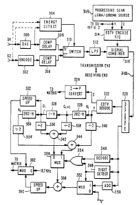
Refer now to Figure 3 which provides an auxiliary
or helper signal formatted as an analog representation of
the temporal dif~erences S1, or alternatively as an
indication of whether vertical or temporal interpolations
(signal S2~ will produce a more accurate reconstructed line
in the receiver. The criterion fox ~electing the helper
signal format is the energy or înformation density of
signal S1. If signal Sl, when band limited ko 750 KH2,
will provide sufficient information to reconstruct the
deleted lines in the receiver, signal S1 is transmitted.
If not, then signal S2, which is a bilevel sisnal, is
compressed using for example run length encoding or
statistical (Hufman) encoding, or a combination of both
and transmitted.
Signal Sl is coupled to the digital-to-analog
converter (DAC3 300 where it is converted to analog form.
DAC 300 may be a multiplying converter and arranged to
provide amplitude compression. Output si~nal from DAC 300
is applied to a signal information density or energy
detector 304 and to the compensating delay eIement 306.
Delay element 306 provides a delay intarval equal to the
intervals over which detector 304 provides energy
calculations and may equal a horizontal line interval, a
field interval or a frame interval for example. Detector
304 may be of the type described in U.S. patent No. 44020I3
entitled "Video Signal Analyzer," which counts the number
of signal txansitions that exceed a predetermin d amplitude
over a predetermined intarval. If the number of
transitions exceeds a preset value detector 304 provides a
logic one output signal for the duration of ~he interval,
otherwise it`provides a logic zero output signal. Note
det~ctor 304 may be realized with digital apparatus in
which case it will be connected ahead of the DAC 300. The
output signal from detector 304 is applied to control a
. .
~L3~
-8- ~C~ 85,111
switching circuit or multiplexer 310. In an alternative
embodiment energy detector 304 may comprise a counter
coupled to count pulses of the signal S2 over a
predetermined interval, and provide an output if the number
of pulses exceeds a predetermined number.
Analog signal S1 from delay element 306 is
coupled to a first signal input terminal of multiplexer
310, the output of which is coupled to the low pass filter
312 having a cutoff fre~uency of e.g. 750 kHz.
Signal S2, which indicates whether a vertically
interpolated or a temporally interpolated signal will more
accurately represent signals representing delet d lines is
coupled to an encoder 302. Encoder 302 may include a run
length encoder followed by a statistical ~such as ~uffman)
encoder to compress the signal S2. Output signal from
encoder 302 is coupled to a second signal input terminal of
multiplexer 310 via a compensatin~ delay element 308 if
required.
Multiple~er 310, in response to the output signal
from detector 304 couples the analog signal Sl to low pass
filter 312 if the energy density of signal Sl is less than
a predetermined level and couples compressed signal S~ to
the low pass filter 312 if the eneryy density of signal S1
exceeds the predetermined level.
The signal from low pass filter 312 is ap~lied to
one input terminal of a signal combiner 316. Video signal,
such as a standard NTSC signal or video siynal from, for
example, an Is~ardi et al. type EDTV encoder 314, from a
source 31S is coupled to a second signal input terminal of
sign~l combiner 316. Lum~a and chroma inputs for encoder
314 are provided by a proyressive scan source 315. Signal
combiner 316 may be of the type which ~uadrature modulates
~ ~he respective input signals onto a picture carrier.
; Alternativaly source 314 may be a souxce of HDTV signals
and signal combiner 316 may include circuitry to combine
the input signals in MAC format. Combined output signal
from signal combiner 318 is ~hen applied to a transmission
channel such as a broadcast transmitter, cable etc.
~3V~
-9~ RCA 85,111
At the receiving end of the system, received
signal is applied to a signal separator 320 which performs
the complementary function of combiner 316. For example if
combiner 316 is a quadrature modulator, then separator 320
is a guadrature demodulator. Separator 320 ~eparates the
helper signal from the encoded video signal. The separated
video sisnal is coupled to a video decoder 322 which
provides separated luminance, Y, and chrominance, C, signal
components in interlace scan format. The chrominance
component, which may be represented by I and Q color
difference signals, are coupled to an
interlace-to-progressive scan converter 324. Converter 324
may be simple speed up circuitry which repeats each line of
chrominance signal at the progressive scan rate. The
chrominance output signals, from converter 324, are coupled
to matrix circuitry (not shown) wherein they are combined
with progressive scan luminance signal to generate R, G and
B color signals to drive a display device.
The separated luminance component signal from
decoder 322 is coupled to an adaptive
interlace~to-progressive scan converter including the
remainder of the circuitry in Figure 3. The luminance
~ignal is applied to the cascade coupled delay elements
326, 328 and 330 which delay signals by 262, 1 and 262
interlace scan intervals respectively. (Two hundred
sixty-two lines corresponds to one field less one half-line
in th~ NTSC systems. In the PAL system, on~ field less one
half-line corresponds to 312 lines.) If the current signal
output from decoder 322 corxesponds to line Bi in Figure 1,
then the output signals from delay elements 326, 328 and
330 correspond to signals from lines Ci+l, Ci and Ai
respectively. The output signal Ci from delay element 328
is applied to a spe~d up circuit 332 which time compresses
the interlace line scan signal to a progr~ssive line scan
interval. The time compressed signal provided by speed up
circuit 332 is coupled to one si~nal input terminal of a
multiplexer 362.
~3~ 2
-10- RCA 85,111
The signals Ci and Ci+1 from delay elements 328
and 326 are coupled, via divide-by-two weighting circuits
336 and 338, to respective input terminals of an adder
circuit 342. The adder circuit 342 produces the sums
(~i + Ci~1)/2 which are coupled to one signal input
terminal of a multiplexer 356. The sums (Ci ~ Ci+l)/2
correspond to vertically interpolated samples representing
deleted lines.
The signals Ai and Bi, from delay element 330 and
decoder 32~ are coupled, via divide-by-two weighting
circuits 334 and 340, to respective input terminals of an
adder circuit 344. The adder circuit 344 produces the sums
(Ai + Bi)/2 which are coupled to a second signal input
terminal of the mul$iplexer 356. The sums (Ai + Bi)/2
correspond to temporally interpolated samples representing
deleted lines.
The multiplexer 356 is controlled by signal from
an OR gate 354 to apply one of the vertically or temporally
interpolated signals to an input terminal of an adder
circuit 358. The adder 358 provides interpolated signals
representing deleted lines of interlace scan duration to a
speed up circuit 360 which time compresses the
interpolated lines to progressive scan in~ervals. Time
compressed signals from speed up circuit 360 are coupled to
a second si~nal input terminal of the multiple~er 362. The
multiplexer 362 is controlled by a sguare wave signal of
interlace scan line rate to alternately couple time
compressed real lines Ci and time compres~ed interpolated
lines from speed up circuit 360 to its output terminal.
The luminanc~ output signal provided by the multiplexer 362
is coupled to the aforementioned matrix circuitry to be
combined with the chrominance signal from converter 324.
In the receiver circuitry so far described it is
presumed that decoder 322 includes analog-to-digital
converter circuitry to convert the received video signal to
digital, e.g., PCM format and that the processing circuitxy
is of digital design.
~ RCA 85,111
The auxiliary or helper signal from signal
separator 320 is coupled to a decoder 346, a digital
detector 348 and an analog~=to-digital converter (ADC) 350.
The decoder 346 performs the complimentary function of the
encoder 302 at the transmitting end of the system. Decoder
346 may include a statistical (e.g. Huffman~ decoder
followed by a run length decoder, and provides the signal
S2 to one input terminal of the OR gate 354. For logic one
and logic zero level values pro~ided by the deco~er 346 the
multiplexer 354 is conditioned to pass the temporally and
vertically interpolated values respectively.
The digital detector 348 determines whether the
helper signal is the digitally compressed signal S2 or the
analog helper signal Sl. This may be accomplished ~y
having the encoder 302 include a recognition signal at the
beginning of each interval of encoded compressed signal.
In this instance the digital detector may be a correlator
designed to recognize the recognition signal and output a
zero level for the following interval. Fox intervals in
which no recognition signal is detected, the digital
detec-tor 348 provides a logic one level output signal.
This function may be incorporated within the decoder 346.
Alternatively the compressed signal S2, at the beginning of
each interval, will of necessity include a relatively dense
bit stream to initiate the decoder. This bit stream will
nominally include far more transitions than ~he analog
helper signal. The digital detector 348 may be desi~ed to
diferentiate the analog and compressed signal formats by
counti~y signal transitions at the beginning o each
3d interval. Since the system will typically be designed to
format the alternative signals in intervals of line, field
or frame periods it is a straight ~orward process to
synchronize the detector to the beginning of each interval
using the horizontal or vertical synchronizing components
of the video signal.
The output signal from the digital detector is
coupled to a second input tenminal of the QR gate 354 and
to the control lnput of a multiplexer 352~ The analog
~3~ 2
-12- RCA 85,111
helper signal after conversion to PCM form in A~C 350 is
coupled to one signal input terminal of multiplexer 352. A
zero valued signal is coupled to a second input terminal of
~he multiplexer 35~. If the received helper signal is the
analog signal, digital detector 348 produces a logic one
output signal which conditions the multiplexer 356 to
couple the temporally interpolated values to the adder 358
and conditions the multiplexer 352 to couple the PCM helper
siynal from ADC 350 to a second input terminal of adder
358. In this instance, the signal provided by adder
circuit 358 is the sum of the helper (xi-(Ai+Bi)/2) plus
the temporally interpolated signal (Ai+Bi)/2) which sum
represent the detected lines xi exactly. Alternatively, if
the received helper signal is the compress~d digital signal
S2, digital detector 348 provides a logic zero valued
output signal which conditions the multiplexer 3S2 to
couple a zero value to the adder 358. In this instance the
multiplexer 356 is controlled by the output of decoder 346
and pro~ides to adder 358 ~he vertically or temporally
interpolated signal which most accurately represents the
deleted lines.
The FIGURE ~ circuitry generate~ alternative
helper signals which are both formatted in compressed
digital form. The ~ll digital helper alternatives require
a significantly smaller d~namic range than the analog
helper an~ thus create significantly less likelihood of
interference with the com~ined video si~nal. In the FIGURE
4 circuit, elements designated with like numbers as
elements in FIGURE 3 are similar elements and perform
similar functions.
Signal S2, which indicates which of the
vertically and temporally interpolated signals will provide
the more accurate representation o the deleted lines at
the receiver, and which indicates which of the signal
differences from subtractors 20 and 32 of FIGURE 2 is
smaller, is coupled to the input terminal of an encoder
400. Encoder 400 may be similar to encoder 300 in FIGU~E 3
and may include~a run length encoder followed by a
~36~4~2
-13- RA 85,111
; statistical encoder. Encoder 400 also includes apparatus
to insert a recognition code at the beginning of each
coding interval. The compressed signal S2 from encoder 400
is coupled to one signal input terminal of a multiplexing
5 switch 410 via a compensating delay element 404.
Signal S2, which is a single bit signal, is
appended as, for example, a least significant bit to
samples of signal S3 which occurs as multibit samplesO In
the combined S2-S3 ~ignal the S2 bit identifies if the S3
sample represents a vertical or temporal difference error.
The co~bined S2-S3 signal is coupled to an encoder 402
- which provides a digitally compressed S2-S3 signal.
Encoder 402 may include a run length encoder followed by a
- statistical decoder. In addition, it includes apparatus to
insert a recognition code at the beginning of each coding
interval. The compxessed signal S2-S3 is coupled to a
second signal input terminal of the multiplexer 410 via
compensating delay element 406.
A counter 408 is coupled to receive the
compressed S2-S3 signal and counts the number of signal
bits in a predetermined interval, e.g., a line interval, a
field interval, etc. If the counted value exceeds a number
which has been determined to exceed the channel capacity
(auxiliary channel), counter 408 generates a logic one
output signal for the coding interval. The output from
counter 408 is coupled to control the multiplexer 410. I~
the number of bits of the compressed S2 S3 signal is lesser
than the channel capacity, the counter conditions the
multiplexer 410 to pass the compressed S2-S3 signal,
convers~ly, if the count exceeds the channel capacity the
; compressed S2 signal is selected. Note the delay elements
404 and 406 provide sufficient signal dalays for the
counter 408 to complete detaction over a coding interval
before the compressed signals arrive at the multiplexer
410. Note also that the signal S3, always represents the
smaller of the vertical and temporal dif~erences and thus
signal 53 can be represented by fewer bits than ware either
'
-14- RCA 85,111
only the vertical or temporal differences utilized as the
error signal.
The output signal from multiplexer 410 is coupled
to the signal combiner 414 wherein it is combined with
video signal from e.g., an EDTV encoder 412. The signal
combiner 414 may be a guadrature modulator which quadrature
modulates a picture carrier with the respective input
signals thereto. The combiner 414 output is coupled via a
transmission path 415 to the receiving portion of the
system.
At the receiving end of the system ~he auxiliary
or helper signal provided by signal separator 320 i~
coupled to first and second decoders 422 and 426 and to a
code type detector 424. The code type detector 424 is
responsive to the inserted recognition codes and generates
signals which are applied to the enable, E, terminals of
the first and second decoders 422 and 426, to enable the
appropriate decoder.
The decoder 422 performs the complementary
function to encoder 400 and provides the signal S2
spatially correlated with the interpolated values provided
by adder circuits 342 and 344. The decoded signal S2 is
coupled to one input terminal of the OR gate 428 to control
the multiplexer 356 when decoder 422 is enabled.
The decoder 426 per~orms the complementary
function to encoder 402 and provides the combined signal
S2-S3 spatially correlated with the interpolatad values
from adder circuits 342 and 344. The signal S2 bit, of the
combined decoded S2~S3 signal, is coupled to a second input
terminal of the OR gate 428 to control the multiple~er 356
when decoder 426 is enabled. The bits representing signal
S3 of ~he decoded S2-S3 signal are coupled to the adder 358
when decoder 426 is enabled and a zero value is coupled to
addar 358 when decoder 426 is disabled.
If the received helper signal corre~ponds to the
signal S2 format, the decoder 422 conditions (with si~nal
S2) the multiplexer 356 to pass the vertical or temporal
interpolated signal which will most closely represent the
~3~S~
-15- RCA 85,111
deleted lines. This signal is coupled unchanged, via adder
358, to the speed up circuitry 360. Alternatively, if the
received helper signal corresponds to the S2-S3 signal
format, the S2 signal from decoder 426 conditions the
multiplexer 356 to pass the vertically or temporally
interpolated signal which most closely repr~sents the
deleted lines to adder 358. The error signal S3 from
decoder 426 is added in adder 358 to the signal provided by
the multiplexer 356. The sums provided by adder 358, in
this instance, exactly represent the signals of the deleted
lines.
In the foregoing description and figures,
compensating delay elements have been omitted to avoid
confusion. For example, if the video decoder 322 is an
EDTV decoder of the Isnardi et al. type, it may be
necessary to include a compensating delay in the helper
signal path to correlate the helper and video ~ignals. In
addition, it may be necessary to include compensating
delays between the signal separator 320 and the decoders
422 and 426 to provide the code type dekector 424 time to
identify the signal format before the helper signal is
applied to the respective decoder. In addition, since the
signal ci from delay element 328 and the generated signal
Xi from adder occur substantially concurrently, the time
compressed versions of signals ci and xi will occur
concurren*ly. Therefore an offset delay of one half an
interlace scan line interval must be provided between
circuit 360 and multiplexex 362. However, one skilled in
the art of circuit design will readily appreciate where
compensating delays are required and he able to include
them.